EP0075825B2 - Elektronisches Postgebührenfeststellsystem - Google Patents
Elektronisches Postgebührenfeststellsystem Download PDFInfo
- Publication number
- EP0075825B2 EP0075825B2 EP82108662A EP82108662A EP0075825B2 EP 0075825 B2 EP0075825 B2 EP 0075825B2 EP 82108662 A EP82108662 A EP 82108662A EP 82108662 A EP82108662 A EP 82108662A EP 0075825 B2 EP0075825 B2 EP 0075825B2
- Authority
- EP
- European Patent Office
- Prior art keywords
- voltage
- transistor
- coupled
- microprocessor
- polarity
- Prior art date
- Legal status (The legal status is an assumption and is not a legal conclusion. Google has not performed a legal analysis and makes no representation as to the accuracy of the status listed.)
- Expired - Lifetime
Links
- 230000015654 memory Effects 0.000 claims description 52
- 238000007639 printing Methods 0.000 claims description 16
- 230000008878 coupling Effects 0.000 claims 7
- 238000010168 coupling process Methods 0.000 claims 7
- 238000005859 coupling reaction Methods 0.000 claims 7
- 239000003990 capacitor Substances 0.000 description 16
- 238000004804 winding Methods 0.000 description 10
- 230000001105 regulatory effect Effects 0.000 description 6
- 239000000872 buffer Substances 0.000 description 4
- 238000012546 transfer Methods 0.000 description 3
- 238000010586 diagram Methods 0.000 description 2
- 238000001914 filtration Methods 0.000 description 2
- 230000006870 function Effects 0.000 description 2
- 238000000034 method Methods 0.000 description 2
- 229910052710 silicon Inorganic materials 0.000 description 2
- 239000010703 silicon Substances 0.000 description 2
- 238000012360 testing method Methods 0.000 description 2
- IJJWOSAXNHWBPR-HUBLWGQQSA-N 5-[(3as,4s,6ar)-2-oxo-1,3,3a,4,6,6a-hexahydrothieno[3,4-d]imidazol-4-yl]-n-(6-hydrazinyl-6-oxohexyl)pentanamide Chemical compound N1C(=O)N[C@@H]2[C@H](CCCCC(=O)NCCCCCC(=O)NN)SC[C@@H]21 IJJWOSAXNHWBPR-HUBLWGQQSA-N 0.000 description 1
- XUIMIQQOPSSXEZ-UHFFFAOYSA-N Silicon Chemical compound [Si] XUIMIQQOPSSXEZ-UHFFFAOYSA-N 0.000 description 1
- 230000015556 catabolic process Effects 0.000 description 1
- 238000010276 construction Methods 0.000 description 1
- 230000001419 dependent effect Effects 0.000 description 1
- 238000013461 design Methods 0.000 description 1
- 230000009977 dual effect Effects 0.000 description 1
- 238000004146 energy storage Methods 0.000 description 1
- 230000007257 malfunction Effects 0.000 description 1
- 230000006386 memory function Effects 0.000 description 1
- 239000002184 metal Substances 0.000 description 1
- 238000012986 modification Methods 0.000 description 1
- 230000004048 modification Effects 0.000 description 1
- 238000010079 rubber tapping Methods 0.000 description 1
- 239000007787 solid Substances 0.000 description 1
- 238000001228 spectrum Methods 0.000 description 1
Images
Classifications
-
- G—PHYSICS
- G07—CHECKING-DEVICES
- G07B—TICKET-ISSUING APPARATUS; FARE-REGISTERING APPARATUS; FRANKING APPARATUS
- G07B17/00—Franking apparatus
- G07B17/00185—Details internally of apparatus in a franking system, e.g. franking machine at customer or apparatus at post office
- G07B17/00362—Calculation or computing within apparatus, e.g. calculation of postage value
-
- G—PHYSICS
- G11—INFORMATION STORAGE
- G11C—STATIC STORES
- G11C16/00—Erasable programmable read-only memories
- G11C16/02—Erasable programmable read-only memories electrically programmable
- G11C16/06—Auxiliary circuits, e.g. for writing into memory
- G11C16/22—Safety or protection circuits preventing unauthorised or accidental access to memory cells
- G11C16/225—Preventing erasure, programming or reading when power supply voltages are outside the required ranges
-
- G—PHYSICS
- G11—INFORMATION STORAGE
- G11C—STATIC STORES
- G11C16/00—Erasable programmable read-only memories
- G11C16/02—Erasable programmable read-only memories electrically programmable
- G11C16/06—Auxiliary circuits, e.g. for writing into memory
- G11C16/30—Power supply circuits
-
- G—PHYSICS
- G11—INFORMATION STORAGE
- G11C—STATIC STORES
- G11C7/00—Arrangements for writing information into, or reading information out from, a digital store
- G11C7/24—Memory cell safety or protection circuits, e.g. arrangements for preventing inadvertent reading or writing; Status cells; Test cells
-
- G—PHYSICS
- G07—CHECKING-DEVICES
- G07B—TICKET-ISSUING APPARATUS; FARE-REGISTERING APPARATUS; FRANKING APPARATUS
- G07B17/00—Franking apparatus
- G07B17/00185—Details internally of apparatus in a franking system, e.g. franking machine at customer or apparatus at post office
- G07B17/00362—Calculation or computing within apparatus, e.g. calculation of postage value
- G07B2017/00395—Memory organization
- G07B2017/00403—Memory zones protected from unauthorized reading or writing
Definitions
- the present invention relates to an electronic postage meter system.
- Electronic postage meter systems have been developed as for example the systems disclosed in US-A-3,978,457 for Microcomputerized Electronic Postage Meter Systems, in US-A-3,938,095 for Computer Responsive Postage Meter and in EP-A-19515, for Electronic Postage Meter Having Improved Security and Fault Tolerance Features.
- Electronic postage meters have also been developed employing plural computing systems. Such a system is shown in US-A-4,301,507, for Electronic Postage Meter Having Plural Computing Systems and assigned to Pitney Bowes Inc.
- the accounting circuits of electronic postage meters include nonvolatile memory capability for storing postage accounting information. This information includes, for example, the amount of postage remaining in the meter for subsequent printing or the total amount of postage printed by the meter. Other types of accounting or operating data may also be stored in the nonvolatile memory.
- the memory function in the electronic accounting circuits have replaced the function performed in previous mechanical-type postage meters by mechanical accounting registers. Postage meters with mechanical accounting registers are not subject to the many problems encountered by electronic postage meters. Conditions cannot normally occur in mechanical-type postage meters that prevent the accounting for printing cylce or which result in the loss of data stored in the registers. Moreover, in mechanical postage meters it is not necessary electronically to monitor the position of the mechanical components associated with printing postage. This, howver, is not the case with electronic postage meters.
- Conditions can occur in electronic postage meters where information stored in electronic accounting circuits can be permanently lost. Conditions such as a total line power failure or fluctuation in voltage conditions can cause the microprocessor associated with the meter to operate erratically and either cause a loss of data or the storage of spurious data in the nonvolatile memory. The loss of data or the storage of spurious data may result in a loss of information representing the postage funds stored in the meter. Since data of this type changes with the printing of postage and is not stored elsewhere outside of the meter, there is no way to recover or reconstruct the lost information. In such a situation, a user may suffer a loss of postage funds.
- EP-A-19515 discloses an electronic postage meter employing a microprocessor and dual redundant battery-backed CMOS memories to store critical meter data.
- the write control lines of the memories are jointly controlled by an output line of the microprocessor and by a voltage sensing circuit in order to prevent writing to the memories during power up and power down conditions.
- the MNOS (metall-nitride-oxide-silicon)-memory device is enabled for writing by applying a -30V DC potential at a write-control line of the memory and the memory is disabled forwriting by only removing this potential.
- microprocessors used in electronic postage meters may be designed to turn off and become inoperative below a predetermined voltage level, such microprocessors may become active again at even lower voltage levels.
- the microprocessors may turn off below a predetermined voltage level and thereafter within a lower range turn on again and be capable of outputting data.
- the microprocessors will again turn off below the lower predetermined range. Because of this unreliable operation at turn off, the accounting information within the postage meter can be destroyed by the inadvertent writing of spurious data during a power down cycle when the microprocessor is believed to be inoperative.
- the cost of carefully testing and selecting microprocessor components for postage meters to avoid this problem can greatly increase the cost of such parts, both because of the cost of testing and because of the rejection of the microprocessor devices that exhibit this characteristic.
- the object of the present invention is to provide an improved electronic postage meter system in which in advertent writing of spurious data into the memory during power-down cycles is substantially overcome.
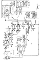
- a postage meter 12 includes: an accounting module 14 having a microprocessor and nonvolatile memory such as a General Instrument Corporation ER3400 type electronically alterable read only memory (this device is described in a General Instrument Corporation manual dated November 1977, entitled EAROM and designated by number 12-11775-1); a printing module 16 having microprocessor and motor control circuits; and a control module 18 having microprocessor and control circuits.
- a control module 18 having microprocessor and control circuits.
- Postage meter 12 includes a series of opto-interrupters 20, 22, 24, 26, and 28.
- the opto-interrupters are used to sense the mechanical position of the parts of the meter.
- the opto-interrupters can be employed to sense the position of a shutter bar which is used to inhibit operation of the meter under certain circumstances, the position of digit wheels of a printer, the home position of a print drum, the position of a bank selector for the print wheels, the position of an interposer, or any other movable mechanical component within the meter.
- These opto-interrupters are coupled to the printing module 16 which monitors and controls the position of the mechanical components of the meter.
- the printing module 16 is connected to the accounting module 14 via a serial data bus 30 and communicates by means of an echoplex technique described in the abovenoted U.S. Patent Application for Electronic Postage Meter Having Plural Computing Systems. Both ends of the bus are buffered by an optics buffer, not shown, which is energized by the power supply +5 volt line to be hereafter described. Similarly, the control module 18 is connected to the accounting module 14 via a serial data bus 32 and also communicates by means of the echoplex technique. Optics buffers, not shown, are provided to buffer the bus. It should be recognized that the particular architecture of the postage meter system is not critical to the present invention. Plural or single microprocessor arrangement may each be employed with the present invention.
- a source of operating voltage such as 110 volt 60 cycle supply, is applied across the meter input terminals 34.
- the voltage is applied to a linear 10.8 volt power supply 36.
- the output from the 10.8 volt linear power supply 36 is supplied to a first 8 volt linear regulated power supply 38 and to a second 5 volt linear regulated power supply 40.
- the 8 volt supply is used to power a display 42 which is operatively coupled via a bus 44 to the control module 18.
- the output from the power supply 40 is directly coupled to the control module 18 and is operated to energize the control module microprocessor.
- the AC operating voltage at terminals 34 is also applied to a silicon controlled rectifier-type, 24 volt power supply 46.
- the regulated output (24 V DC) from the power supply 46 is applied to a printwheel bank stepper motor 48 and a printwheel stepper motor 50 associated with the printing module 16.
- the regulated output is also coupled by an AC choke 52 to a capacitor 54.
- the internal capacitance within the 24 volt power supply 46 provides sufficient energy storage to continue to properly energize a switching regulator 56 should an AC power failure occur at terminals 34.
- the accounting module microprocessor 58 transfers information from the postage meter volatile memory (which may be internal or external to the microprocessor) via the data bus 66 to a nonvolatile memory 62.
- the switching regulator 56 in conjunction with a transformer with related circuitry, provide regulated output voltages used to energize the accounting module.
- a supply of plus five volts is developed by regulator 56 and is applied to the accounting module microprocessor 58, to NMOS nonvolatile memory 62, to the optic buffers (not shown) for the serial data bus 30 connected between the accounting and printing modules, to the printing module 16, and to the opto-interrupters 20-28.
- a supply of minus 30 volts is also developed across Zener diode 88 via transformer secondary 78 and is applied via an NPN transistor 100 and an NPN transistor 64 to the nonvolatile memory 62. The operation of transistor 64 is controlled by the accounting module microprocessor 58.
- the minus 30 volts is required in conjunction with a minus 12 volts (which is developed from a tapping 90 of the transformer and applied to the nonvolatile memory 62) and the plus five volts to enable the nonvolatile memory to have data written into the device.
- the switching regulator 56 functions to selectively apply the 24 volts developed across the capacitor 54 to the junction of a diode 66 and poled transformer primary winding 68.
- the frequency at which the regulator 56 operates or switches is determined by a capacitor 70 which controls the operating frequency of the supply.
- Primary winding 68 is further coupled to ground by a capacitor 72.
- Diode 66 and capacitor 72 form a complete circuit in parallel with the primary winding 68.
- the circuit path is through a point of fixed reference potential, here shown as ground.
- a voltage of +5 volts is developed across capacitor 72.
- This voltage is sensed and coupled via a series connected variable resistor 74 and a fixed resistor 76 to an input terminal on the switching regulator 56.
- This feed-back path controls the supply 56 to maintain a constant voltage across capacitor 72.
- a voltage variation of appoximately 10 millivolts can occur across the capacitor 72.
- the step-up secondary winding 78 oppositely poled to the primary winding 68 is electromagnetically coupled via a mol- lypermoly core 80 to the primary winding 68.
- the secondary winding 78 is connected to ground at one end and has its opposite end coupled via a diode 82 which operates in conjunction with a capacitor 84 and current limiting resistor 86 to develop -30 volts across Zener diode 88 as already mentioned.
- Acenter-tap 90 on the secondary winding 78 is connected to a diode 92 which operates in conjunction with a capacitor 94 and a current limiting resistor 96 to develop -12 volts across a Zener diode 98.
- a circuit is provided to ensure that the nonvolatile memory 62 is not energized by the -30 volts necessary for a writing operation after a particular voltage condition in the power down sequence has been reached. This ensures that even if data is put onto the nonvolatile memory bus 66 by the microprocessor 62, the data will not be written into the nonvolatile memory. This is particularly important because, although the micro-processor may be designed to turn off and not output data at a determined voltage level (for example, when the +5 volt supply drops below voltage +4.50 volts), it has been discovered that such microprocessors may become active again at even lower voltages such as +3 volts.
- the -30 volt supply to the nonvolatile memory 62 is passed through the collector-emitter electrode current path of the NPN transistor 100.
- the collector electrode of the transistor is coupled via a resistor 102 to the +5 volts developed at capacitor 72.
- Base bias for the transistor 100 is obtained from a PNP transistor 104.
- the emitter electrode of the transistor 104 is connected by a 10 voltzenerdiode 106 to the +24 volt DC supply 46.
- a resistor 109 provides a ground return for transistor 104.
- Resistors 108 and 110 are connected to the base electrode of transistor 100.
- a capacitor 112 is provided to further filter transients.
- a power down routine is initiated.
- the routine may be initiated by a system such as that disclosed in the aforementioned US-A-4,285,050 for Electronic Postage Meter Operating Voltage Variation Sensing System.
- transistor 104 is biased out of conduction.
- transistor 100 is also biased out of conduction. This causes the +5 volts applied via resistor 102 to the collector electrode of transistor 100 to be applied to the emitter electrode of transistor 64.
- the +5 volts reverse biases transistor 64 and ensures that no information can be written into the nonvolatile memory 62 during the remainder of the power down cycle, as a supply of -30 volts is required to enable a WRITE operation in the nonvola- tive memory.
- Transistor 64 continues to be reverse biased through the decay cycle, until the voltage falls below the junction potential of the device, normally +.7 volts. By this time, however, the microprocessor has passed through the range of uncertain operating voltage and is completely inoperative. By this means, a further enhanced security is provided in the operation of the nonvolatile memory 62 and, additionally, a wider spectrum of microprocessor devices with concomitant cost advantages can be employed in the postage meter.
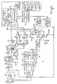
- resistor 111 is added to the schematic circuit diagram shown in Figure 1 to apply the +5 volt supply directly to the WRITE voltage terminal.
- resistor 111 is connected between the collector electrode of transistor 64 and capacitor 72. This provides yet further enhanced memory protection over the circuit shown in Figure 1.
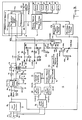
- transistor 64 shown in Figures 1 and 2 is eliminated and the collector electrode of transistor 100 is directly connected to the WRITE voltage terminal.
- the structure eliminates the redundant protection afforded by both transistor 64 whose base bias is controlled by microprocessor 58 and transistor 100 whose base bias is dependent upon voltage levels in the postage meter's power supply systems. Protection is afforded in this case by control over the conductivity of the collector-emitter electrode current path of transistor 100.
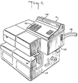
- FIG. 4 is a per- sective view of an electronic postage meter suited to incorporate apparatus according to the present invention.
- the postage meter 12 is detachably secured to a base unit 114 so as to form a letter slot 116 therebetween at the front edge of the assembly.
- the base unit 114 may be mechanically of the type disclosed, for example, in US-A-2,934,009 issued to Bach et al for Sheet Feeding and Treating.
- the base incorporates a mechanical drive, not shown, for providing mechanical drive energy for the printing drum of meter 12.
- the postage meter 12 is an electronic postage meter in the sense that the accounting system within the meter, including the registers, is electronic as opposed to mechanical.
- Power is suppoied to the meter 12 via an AC power cord 118.
- the power cord 118 is connected to terminal 34 within the conductive shielding provided by the metal meter housing 120.
- a keyboard 122 and display 124 are provided and are connected to the control module 18 microprocessor and control circuit.
- the protection circuit ensures that information is not inadvertently written into a nonvolatile memory, which memory is particularly suitable for use as part of an electronic postage meter system. This form of proctection is particularly important in electronic postage meter systems with regard to ensuring the integrity of accounting data stored in the meter.
- the present invention ensures that erroneous information is not written into nonvolatile memory during a power down cycle.
- a nonvolatile memory including a WRITE voltage (V GG ) terminal which when energized by a first predetermined polarity voltage enables the nonvolatile memory to have data written into memory locations.
- a computing means is operatively coupled to the nonvolatile memory for writing data into such memory location.
- First means are provided for generating a voltage of the first predetermined polarity, and second means are also provided for generating a second voltage differing from the voltage of the first predetermined polarity.
- Means are coupled to the first voltage generating means, the second voltage generating means and the WRITE voltage terminal of the nonvolatile memory for applying the voltage of the first polarity to the WRITE voltage terminal when a predetermined power condition exists and for utilizing the second voltage for causing a different voltage level from the first predetermined voltage to be applied to the WRITE voltage terminal when the predetermined power condition is not present.
- the control of the voltage levels applied to the WRITE voltage terminal is independent of the operation of the computing means. Thus, protection can be provided against improper data being written into the nonvolatile memory even if the computing means malfunctions during a power down operation.
Landscapes
- Physics & Mathematics (AREA)
- Engineering & Computer Science (AREA)
- Mathematical Physics (AREA)
- Theoretical Computer Science (AREA)
- General Physics & Mathematics (AREA)
- Computer Security & Cryptography (AREA)
- Devices For Checking Fares Or Tickets At Control Points (AREA)
- Techniques For Improving Reliability Of Storages (AREA)
Claims (10)
dadurch gekennzeichnet, daß
die Schalteinrichtung ein Eingangstransistor (64) ist, dessen Steuerelektrode an den Mikroprozessor gekoppelt ist.
gekennzeichnet durch einen Widerstand (111), der zwischen den WRITE-Spannungzuführanschluß und die zweite Spannungerzeugungseinrichtung angeschlossen ist.
dadurch gekennzeichnet, daß
die Schalteinrichtung (100) ein Transistor ist, dessen steuerbarer Pfad zwischen die ersten Spannungerzeugungseirichtung und die WRITE-Spannungsleitung gekoppelt ist.
gekennzeichnet durch eine Einrichtung (108, 110) zum Koppeln des Steueranschlusses des Transistors (100) an die Fühlereinrichtung (104, 106,109) derart, daß die Fühlereinrichtung, die Leitfähigkeit des steuerbaren Pfads des Transistors (100) steuert.
dadurch gekennzeichnet, daß
die Fühlereinrichtung einen Kopplungstransistor (104) umfaßt, der zwischen die erste Spannungerzeugungseinrichtung und eine Quelle (46) einer DC-Betriebsleistung gekoppelt ist, mit Energie versorgbar durch die externe Quelle (34) der Betriebspannung, wobei der Kopplungstransistor (104) angeordnet ist, um die Vorspannung, die der Steuerelektrode des Schalteinrichtungstransistors (100) zugeführt wird, zu steuern.
dadurch gekennzeichnet, daß
der steuerbare Pfad des Kopplungstransistors (104) in Reihe mit einer Zener-Diode (106) verbunden ist, wobei die Reihenschaltung zwischen die erste Spannungerzeugungseinrichtung (92,934,96,98) und die DC-Leistungsquelle (46) verbunden ist.
dadurch gekennzeichnet, daß
die Kopplungseinrichtung eine Impedanz (102) ist.
Applications Claiming Priority (2)
| Application Number | Priority Date | Filing Date | Title |
|---|---|---|---|
| US06/306,979 US4445198A (en) | 1981-09-29 | 1981-09-29 | Memory protection circuit for an electronic postage meter |
| US306979 | 1999-05-07 |
Publications (4)
| Publication Number | Publication Date |
|---|---|
| EP0075825A2 EP0075825A2 (de) | 1983-04-06 |
| EP0075825A3 EP0075825A3 (en) | 1984-12-19 |
| EP0075825B1 EP0075825B1 (de) | 1988-09-28 |
| EP0075825B2 true EP0075825B2 (de) | 1993-06-09 |
Family
ID=23187733
Family Applications (1)
| Application Number | Title | Priority Date | Filing Date |
|---|---|---|---|
| EP82108662A Expired - Lifetime EP0075825B2 (de) | 1981-09-29 | 1982-09-20 | Elektronisches Postgebührenfeststellsystem |
Country Status (5)
| Country | Link |
|---|---|
| US (1) | US4445198A (de) |
| EP (1) | EP0075825B2 (de) |
| JP (1) | JP2532356B2 (de) |
| CA (1) | CA1188421A (de) |
| DE (1) | DE3279076D1 (de) |
Families Citing this family (28)
| Publication number | Priority date | Publication date | Assignee | Title |
|---|---|---|---|---|
| US4547853A (en) * | 1982-10-13 | 1985-10-15 | Pitney Bowes Inc. | Electronic postage meter reset circuit |
| US4509141A (en) * | 1982-12-08 | 1985-04-02 | Pitney Bowes Inc. | Postage meter with keyboard keys used for changing operating constants |
| US4534018A (en) * | 1983-04-29 | 1985-08-06 | Pitney Bowes Inc. | Non-volatile memory protection circuit with microprocessor interaction |
| US4591976A (en) * | 1983-06-17 | 1986-05-27 | The United States Of America As Represented By The Secretary Of The Air Force | Multiple task oriented processor |
| US4578774A (en) * | 1983-07-18 | 1986-03-25 | Pitney Bowes Inc. | System for limiting access to non-volatile memory in electronic postage meters |
| US4712139A (en) * | 1983-10-28 | 1987-12-08 | Canon Kabushiki Kaisha | Image communication apparatus |
| US4627016A (en) * | 1984-08-22 | 1986-12-02 | Pitney Bowes Inc. | Memory address location system for an electronic postage meter having multiple non-volatile memories |
| US4731749A (en) * | 1984-08-22 | 1988-03-15 | Pitney Bowes Inc. | Electronic postage meter having multiple non-volatile memories for storing different historical information reflecting postage transactions |
| EP0173249B2 (de) * | 1984-08-22 | 1998-07-08 | Pitney Bowes Inc. | Nichtflüchtiges Speichersystem mit Echtzeit- und Netzausfall-Datenspeicherfähigkeit für eine Frankiermaschine |
| US4607351A (en) * | 1985-01-14 | 1986-08-19 | International Business Machine Corp. | Cartridge memory protection |
| US4845632A (en) * | 1985-10-16 | 1989-07-04 | Pitney Bowes Inc. | Electonic postage meter system having arrangement for rapid storage of critical postage accounting data in plural nonvolatile memories |
| US4805109A (en) * | 1985-10-16 | 1989-02-14 | Pitney Bowes Inc. | Nonvolatile memory protection arrangement for electronic postage meter system having plural nonvolatile memories |
| US4817004A (en) * | 1985-10-16 | 1989-03-28 | Pitney Bowes Inc. | Electronic postage meter operating system |
| US4807141A (en) * | 1985-12-16 | 1989-02-21 | Pitney Bowes Inc. | Postage meter with microprocessor controlled reset inhibiting means |
| US4926340A (en) * | 1986-07-10 | 1990-05-15 | Rosemount Inc. | Low power process measurement transmitter |
| US4800532A (en) * | 1987-11-25 | 1989-01-24 | Siemens Aktiengesellschaft | Circuit arrangement with a processor and at least two read-write memories |
| US5349669A (en) * | 1988-12-21 | 1994-09-20 | Oki Electric Industry Co., Ltd. | Data write control means |
| US5021963A (en) * | 1988-12-30 | 1991-06-04 | Pitney Bowes Inc. | EPM having an improvement in accounting update security |
| US5297119A (en) * | 1990-11-30 | 1994-03-22 | Casio Computer Co., Ltd. | Data storage apparatus |
| EP0488354B1 (de) * | 1990-11-30 | 1997-05-14 | Casio Computer Company Limited | Datenspeicheranordnung |
| US5634000A (en) * | 1991-07-31 | 1997-05-27 | Ascom Autelca Ag | Power-fail return loop |
| GB9126998D0 (en) * | 1991-12-19 | 1992-02-19 | Alcatel Business Machines Limi | Franking machine |
| US5712542A (en) * | 1995-05-25 | 1998-01-27 | Ascom Hasler Mailing Systems Ag | Postage meter with improved handling of power failure |
| US5749078A (en) * | 1996-08-23 | 1998-05-05 | Pitney Bowes Inc. | Method and apparatus for storage of accounting information in a value dispensing system |
| GB2321123B (en) * | 1997-01-11 | 2001-01-03 | Motorola Ltd | Circuit for erasing a memory and a method thereof |
| DE10221579A1 (de) * | 2002-05-08 | 2003-12-04 | Siemens Ag | Elektronische Speichereinrichtung für Kenngrößen und Umrechnungsfaktoren für elektronische Schutzeinrichtungen von Leistungsschaltern |
| DE10221571A1 (de) * | 2002-05-08 | 2003-12-04 | Siemens Ag | Elektrischer Leistungsschalter mit einem elektronischen Speicher für Kenngrößen und/oder Umrechnungsfaktoren |
| US7675257B2 (en) * | 2007-03-09 | 2010-03-09 | Regal Beloit Corporation | Methods and systems for recording operating information of an electronically commutated motor |
Family Cites Families (9)
| Publication number | Priority date | Publication date | Assignee | Title |
|---|---|---|---|---|
| US2934009A (en) * | 1956-10-22 | 1960-04-26 | Pitney Bowes Inc | Sheet feeding and treating |
| US3938095A (en) * | 1971-11-04 | 1976-02-10 | Pitney-Bowes, Inc. | Computer responsive postage meter |
| US3810116A (en) * | 1972-11-24 | 1974-05-07 | Sperry Rand Corp | Volatile memory protection |
| US3978457A (en) * | 1974-12-23 | 1976-08-31 | Pitney-Bowes, Inc. | Microcomputerized electronic postage meter system |
| CA1160744A (en) * | 1979-05-09 | 1984-01-17 | Jesse T. Quatse | Electronic postage meter having improved security and fault tolerance features |
| US4285050A (en) * | 1979-10-30 | 1981-08-18 | Pitney Bowes Inc. | Electronic postage meter operating voltage variation sensing system |
| US4301507A (en) * | 1979-10-30 | 1981-11-17 | Pitney Bowes Inc. | Electronic postage meter having plural computing systems |
| US4287825A (en) * | 1979-10-30 | 1981-09-08 | Pitney Bowes Inc. | Printing control system |
| US4337524A (en) * | 1980-02-07 | 1982-06-29 | Mostek Corporation | Backup power circuit for biasing bit lines of a static semiconductor memory |
-
1981
- 1981-09-29 US US06/306,979 patent/US4445198A/en not_active Expired - Lifetime
-
1982
- 1982-09-20 EP EP82108662A patent/EP0075825B2/de not_active Expired - Lifetime
- 1982-09-20 DE DE8282108662T patent/DE3279076D1/de not_active Expired
- 1982-09-24 CA CA000412167A patent/CA1188421A/en not_active Expired
- 1982-09-29 JP JP57170819A patent/JP2532356B2/ja not_active Expired - Lifetime
Also Published As
| Publication number | Publication date |
|---|---|
| JPS5868186A (ja) | 1983-04-22 |
| EP0075825A3 (en) | 1984-12-19 |
| US4445198A (en) | 1984-04-24 |
| EP0075825A2 (de) | 1983-04-06 |
| JP2532356B2 (ja) | 1996-09-11 |
| CA1188421A (en) | 1985-06-04 |
| DE3279076D1 (en) | 1988-11-03 |
| EP0075825B1 (de) | 1988-09-28 |
Similar Documents
| Publication | Publication Date | Title |
|---|---|---|
| EP0075825B2 (de) | Elektronisches Postgebührenfeststellsystem | |
| EP0124092B1 (de) | Elektronische Frankiermaschine und Datenlösch- und -schreibverfahren in einem nichtflüchtigen Speicher | |
| EP0106320B1 (de) | Elektronische Frankiermaschine mit Rücksetzschaltkreis | |
| US4578774A (en) | System for limiting access to non-volatile memory in electronic postage meters | |
| US4285050A (en) | Electronic postage meter operating voltage variation sensing system | |
| US4998203A (en) | Postage meter with a non-volatile memory security circuit | |
| EP0173249B1 (de) | Nichtflüchtiges Speichersystem mit Echtzeit- und Netzausfall-Datenspeicherfähigkeit für eine Frankiermaschine | |
| US4845632A (en) | Electonic postage meter system having arrangement for rapid storage of critical postage accounting data in plural nonvolatile memories | |
| EP0197345B1 (de) | Elektronische Frankiermaschine mit Einschalt- und Ausschalt-Schutzschaltkreis | |
| US4706215A (en) | Data protection system for electronic postage meters having multiple non-volatile multiple memories | |
| US4472781A (en) | Power supply system | |
| US4701856A (en) | Reset delay circuit for an electronic postage meter | |
| EP0222197B1 (de) | Systeme zur nichtflüchtigen Speicherung von Daten und Frankiermaschinensysteme | |
| CA1264376A (en) | Method and apparatus for locating and displaying historical information within an electronic postage meter | |
| US4578758A (en) | Electronic postage meter having a regulated power supply system responsive to a voltage developed in a transformer primary winding circuit | |
| CA1211790A (en) | Power supply system | |
| CA1247254A (en) | Postage meter with a non-volatile memory security circuit | |
| JP3305105B2 (ja) | 画像形成装置 |
Legal Events
| Date | Code | Title | Description |
|---|---|---|---|
| PUAI | Public reference made under article 153(3) epc to a published international application that has entered the european phase |
Free format text: ORIGINAL CODE: 0009012 |
|
| AK | Designated contracting states |
Designated state(s): CH DE FR GB LI |
|
| RAP1 | Party data changed (applicant data changed or rights of an application transferred) |
Owner name: PITNEY BOWES, INC. |
|
| PUAL | Search report despatched |
Free format text: ORIGINAL CODE: 0009013 |
|
| AK | Designated contracting states |
Designated state(s): CH DE FR GB LI |
|
| 17P | Request for examination filed |
Effective date: 19850419 |
|
| 17Q | First examination report despatched |
Effective date: 19860402 |
|
| RAP1 | Party data changed (applicant data changed or rights of an application transferred) |
Owner name: PITNEY BOWES INC. |
|
| GRAA | (expected) grant |
Free format text: ORIGINAL CODE: 0009210 |
|
| AK | Designated contracting states |
Kind code of ref document: B1 Designated state(s): CH DE FR GB LI |
|
| REF | Corresponds to: |
Ref document number: 3279076 Country of ref document: DE Date of ref document: 19881103 |
|
| ET | Fr: translation filed | ||
| PLBI | Opposition filed |
Free format text: ORIGINAL CODE: 0009260 |
|
| 26 | Opposition filed |
Opponent name: FRANCOTYP-POSTALIA GMBH Effective date: 19890616 |
|
| PUAH | Patent maintained in amended form |
Free format text: ORIGINAL CODE: 0009272 |
|
| STAA | Information on the status of an ep patent application or granted ep patent |
Free format text: STATUS: PATENT MAINTAINED AS AMENDED |
|
| 27A | Patent maintained in amended form |
Effective date: 19930609 |
|
| AK | Designated contracting states |
Kind code of ref document: B2 Designated state(s): CH DE FR GB LI |
|
| REG | Reference to a national code |
Ref country code: CH Ref legal event code: AEN |
|
| ET3 | Fr: translation filed ** decision concerning opposition | ||
| PGFP | Annual fee paid to national office [announced via postgrant information from national office to epo] |
Ref country code: FR Payment date: 20010831 Year of fee payment: 20 Ref country code: DE Payment date: 20010831 Year of fee payment: 20 |
|
| PGFP | Annual fee paid to national office [announced via postgrant information from national office to epo] |
Ref country code: CH Payment date: 20010903 Year of fee payment: 20 |
|
| PGFP | Annual fee paid to national office [announced via postgrant information from national office to epo] |
Ref country code: GB Payment date: 20010904 Year of fee payment: 20 |
|
| REG | Reference to a national code |
Ref country code: GB Ref legal event code: IF02 |
|
| PG25 | Lapsed in a contracting state [announced via postgrant information from national office to epo] |
Ref country code: LI Free format text: LAPSE BECAUSE OF EXPIRATION OF PROTECTION Effective date: 20020919 Ref country code: GB Free format text: LAPSE BECAUSE OF EXPIRATION OF PROTECTION Effective date: 20020919 Ref country code: CH Free format text: LAPSE BECAUSE OF EXPIRATION OF PROTECTION Effective date: 20020919 |
|
| REG | Reference to a national code |
Ref country code: GB Ref legal event code: PE20 Effective date: 20020919 |
|
| REG | Reference to a national code |
Ref country code: CH Ref legal event code: PL |
|
| PLAB | Opposition data, opponent's data or that of the opponent's representative modified |
Free format text: ORIGINAL CODE: 0009299OPPO |