EP0072542A2 - Egaliseur adaptatif - Google Patents
Egaliseur adaptatif Download PDFInfo
- Publication number
- EP0072542A2 EP0072542A2 EP82107347A EP82107347A EP0072542A2 EP 0072542 A2 EP0072542 A2 EP 0072542A2 EP 82107347 A EP82107347 A EP 82107347A EP 82107347 A EP82107347 A EP 82107347A EP 0072542 A2 EP0072542 A2 EP 0072542A2
- Authority
- EP
- European Patent Office
- Prior art keywords
- equalizer
- fade
- signal
- frequency
- stages
- Prior art date
- Legal status (The legal status is an assumption and is not a legal conclusion. Google has not performed a legal analysis and makes no representation as to the accuracy of the status listed.)
- Withdrawn
Links
Images


Classifications
-
- H—ELECTRICITY
- H04—ELECTRIC COMMUNICATION TECHNIQUE
- H04B—TRANSMISSION
- H04B3/00—Line transmission systems
- H04B3/02—Details
- H04B3/04—Control of transmission; Equalising
- H04B3/14—Control of transmission; Equalising characterised by the equalising network used
- H04B3/143—Control of transmission; Equalising characterised by the equalising network used using amplitude-frequency equalisers
- H04B3/145—Control of transmission; Equalising characterised by the equalising network used using amplitude-frequency equalisers variable equalisers
-
- H—ELECTRICITY
- H04—ELECTRIC COMMUNICATION TECHNIQUE
- H04B—TRANSMISSION
- H04B7/00—Radio transmission systems, i.e. using radiation field
- H04B7/005—Control of transmission; Equalising
Definitions
- This invention relates to signal equalizers and, in particular, to adaptive fade equalizers.
- the problem is that signal fading resulting from multipath transmission is basically unpredictable. Accordingly, the compensation introduced by a fade equalizer must be capable of automatically adapting to the changing signal conditions.
- One such adaptive equalizer which employs feedback techniques, compensates for amplitude distortion. However, it does not provide delay equalization in the case of nonminimum phase fades. Indeed, for a nonminimum phase fade, the delay distortion is doubled.
- all-pass networks which are more difficult to realize, are used to compensate the delay distortion for both minimum and nonminimum phase fades.
- an adaptive equalizer in accordance with the present invention, comprises a cascade of feed-forward stages, each one of which includes: a first parallel wavepath including a first adjustable attenuator; a second parallel wavepath including a second adjustable attenuator and an adjustable delay network; and means for combining the signals in the two wavepaths in a common output.
- control means When used as an adaptive fade equalizer, control means are provided for adjusting the equalizer parameters in response to changes in the fade characteristics.
- the stages can be adjusted simultaneously.
- the delay elements can be fixed and the fade notch translated into frequency coincidence with the equalizer bump frequency.
- simultaneous amplitude and delay equalization of the received signal is produced for both minimum and nonminimum phase fades.
- feed-forward sections instead of feedback, instability problems during nonminimum phase fades are avoided.
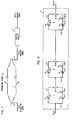
- FIG. 1 shows a portion of a radio communication system including a transmission source 9, a multipath transmission medium 10 and, at the receiver 8, an adaptive equalizer 11.
- the transmission medium 10 can be reasonably represented by a two-path model.
- medium 10 is shown to include a direct path 15 between the transmission source and the receiver, and an indirect path 16.
- the former is characterized by a gain factor a.
- the latter is characterized by a relative delay T and a gain factor a, where T , a and a vary as functions of time.
- the total received signal R(jw) includes a direct path component and an indirect path component and is given by
- the transmission medium when the amplitude of the delayed signal is less than that of the direct signal (i.e., b ⁇ l), the transmission medium is a so-called "minimum phase shift network.” When the amplitude of the delayed signal is greater than the direct path signal (i.e., b>l), the medium has the characteristics of a "nonminimum phase shift network.” (For a discussion of minimum phase shift networks, see “Network Analysis and Feedback Amplifier Design," by H. W. Bode, published by D. Van Nostrand Company, Inc. of New York, Fourth Printing, pp. 242 et seq.)
- a fade notch occurs when the two received signal components destructively interfere.
- the function of the equalizer is to reduce the inband amplitude and delay distortion produced by the fade such that the equalized signal, E N (j w ), at the output of the equalizer is substantially the same as the transmitted signal T(jw).
- FIG. 2 shows an adaptive equalizer in accordance with the present invention comprising N feed-forward stages.
- Each stage comprises: a first parallel wavepath 1-1, 1-2 ... 1-N including a first adjustable attenuator 20-1, 20-2 ... 20-N such as, for example, a PIN diode; wavepath 2-1, 2-2 ... 2-N including a second adjustable attenuator 21-1, 21-2 ... 21-N, and an adjustable delay means 22-1, 22-2 ... 22-N; and means 23-1, 23-2 ... 23-N for combining the signals in the two wavepaths.
- the combined signal in each of the first N-1 stages is coupled to the next stage in the equalizer.
- the combined signal from the last stage, E N (jw) is the equalizer output signal.
- the first stage differs from the other N-l stages in that the signal combiner 23-1 forms a difference signal whereas combiners 23-2 ... 23- N form sum signals. The reason for this difference will become apparent in the discussion that follows.
- the output signal E 1 (j ⁇ ) of the first equalizer stage is the difference in the signals in the two paths 1-1 and 2-1 given by where a 1 and b 1 are the attenuator gain factors for the respective wavepaths.
- the equalizer output signal is simply a scaled (i.e., totally equalized) replica of the transmitted signal. This is the equivalent of a flat fade which can be compensated by the AGC system in the receiver.
- Equation (8) reduces to where aCK 2N is a frequency independent term and e -j ⁇ 2NT is a linear phase term.
- the equalizer eliminates the frequency selective nature of the transmission medium due to multipath transmission.
- the number of stages required is given by
- a 40 dB fade which is composed of a 20 dB flat fade and a selective fade of only 20 dB.
- a 5 stage equalizer will yield the same degree of equalization as the 8 stages operating on a 40 dB selective fade.
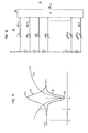
- FIG. 3 illustrates, in block diagram, one embodiment of an arrangement for adjusting the equalizer parameters so as to accommodate such changing signal conditions when the equalizer is used to compensate for multipath fades.
- the control algorithm can be simplified by fixing the delay elements 22-1, 22-2 ... 22-N.
- the gain bump of the equalizer occurs at a fixed frequency. This means that the location (i.e., frequency) of the fade notch must be detected and then translated so that in all cases it is aligned with the equalizer gain bump frequency.
- the gain of the equalizer is adjusted such that it equals the magnitude of the selective fade portion of the fade.
- the equalizer 11 is located between an input frequency converter 43 and an output frequency converter 44 which serve to translate the signal fade notch frequency into coincidence with the equalizer bump frequency, and then back to within the IF band. Both converters receive a signal from a common voltage controlled local oscillator 45 whose output frequency is determined by a frequency error signal derived from a controller 50.
- the equalized spectrum will display an "S" shaped amplitude response.
- the spectrum at the output of the equalizer is examined at frequencies surrounding the equalizer bump frequency f ee This is done by the two bandpass filters 39 and 40 which are tuned to frequencies f e+ and f e- , respectively, where f e- is a frequency below f e , and f e+ is a frequency above f ee
- the filter outputs are coupled to the controller which develops the appropriate compensating error signal for changing the oscillator frequency.
- the location of the fade notch is determined by sampling the input signal at three frequencies, f l , f 2 and f 3 , within the band of interest, where f 2 is at band center and f, and f 3 are advantageously as close to the band edges as possible. Sampling is accomplished by feeding a portion of the input signal to each of three bandpass filters 32, 33 and 34 tuned, respectively, to f l , f 2 and f 3 . The three filter outputs are coupled to controller 50.
- a second determination to be made is whether or not there is a minimum or nonminimum phase fade.
- This information is required by the controller in order to set the relative gain factors ⁇ a i ⁇ and ⁇ b i ⁇ of the equalizer stages.
- ⁇ a i ⁇ is advantageously set equal to unity, with ⁇ b i ⁇ adjusted to values less than one.
- ⁇ b i ⁇ is advantageously set equal to unity with ⁇ a i ⁇ made less than one.
- the information required to make this determination is obtained by sampling the signal at the input to the equalizer. The determination is made in a phase analyzer 51, which communicates the results of the determination to controller 50.
- the three sampled frequencies f l , f 2 and f 3 are compared at the output of the output converter and the information thus derived is used to update the gain coefficients ⁇ a i ⁇ and ⁇ b i ⁇ .
- the output signal is sampled by bandpass filters 36, 37 and 38, and the sampled signals, thus obtained, are coupled to the controller.
- FIG. 4 shows, in block diagram, the portion of the controller 50 concerned with determining the fade notch frequency, f n , and adjusting the frequency of the local oscillator 45 so as to shift the fade notch into frequency coincidence with the equalizer bump frequency, f ee
- the spectral power of the input signal is measured at three points. It can be shown that, based upon these measurements, the fade notch frequency can be approximated by where f c is the frequency at band center;
- the fade notch detector and oscillator control voltage generator It is the function of the fade notch detector and oscillator control voltage generator to generate a control voltage that will produce frequency changes in oscillator 45 that are proportional to f n . Accordingly, the outputs from bandpass filters 32, 33 and 34 are coupled, respectively, to power detectors 72, 71 and 70 whose outputs are , and . Signals and are combined in differential amplifier 75 to produce signal - . Signal is amplified and inverted in amplifier 73 to produce signal -2 , which is then combined with signals and in summing network 74 to produce signal + -2 . The output of amplifier 75 is then divided in divider 76 by the output from summing network 74 to produce signal component A given by
- Signal component A is then multiplied in multiplier 77 by a voltage v ⁇ f/2 that is proportional to ⁇ f/2, and the resulting product added, in a summing network 78, to a second voltage v c that is proportional to f c .
- the resulting signal, v f , at the output of summing network 78 is then where v f is proportional to f n , as given by equation (13).
- a voltage v (fe-fc) is applied to the oscillator such that the local oscillator frequency, f o , applied to the frequency converters 43 and 44 is
- the function of the oscillator control voltage is to shift that frequency an amount f c -f n , so that the fade notch, rather than band center, is in frequency coincidence with the equalizer bump frequency. Accordingly, an incremental voltage ⁇ v proportional to f c -f n is required. (For purposes of this discussion, it is assumed that the oscillator output frequency is proportional to the control voltage over the range of interest.) This control voltage is obtained by multiplying v f by -1 in a multiplier 79, and adding voltage v c to the result in summing network 80. The resulting signal ⁇ v is then given by which is proportional to f c -f n as required.
- the outputs from bandpass filters 39 and 40 are coupled to a pair of power detectors 81 and 82.
- the outputs P e+ and P e- from the latter are coupled, in turn, to an integrator 83 which generates a signal that is proportional to the difference in the signal power, integrated over a period of time.
- This integrated signal is applied to summing network 80 and serves as a vernier adjustment of the oscillator control voltage ⁇ v.
- the delay response is a maximum at the notch frequency, decreasing symmetrically as a function of frequency, as shown by curve 85. If, on the other hand, it is a nonminimum phase fade, the delay response is a minimum at the notch frequency, increasing as a function of frequency, as illustrated by curve 86.
- the delay T(f n ) at the fade notch frequency f n is compared with the delay ⁇ (f' n ) at a frequency f' n , symmetry located on the other side of the band center frequency, f c , the nature of the fade can be determined. That is, if it is a minimum phase fade, whereas if it is a nonminimum phase fade.
- the phase analyzer comprises two delay sensors 105 and 106, as illustrated in FIG. 6. Noting that the delay is equal to the derivative of the phase angle with respect to frequency, delay sensor 105 evaluates the phase angle at the fade notch frequency f n and at a frequency f n + ⁇ f, where ⁇ f is relatively small, and then takes their difference to obtain a measure of the delay. It then does the same thing at f' n and compares the two delays.
- a component of the signal R(jw) is multiplied, in a mixer 91 located in delay sensor 105, by a signal cos 2 ⁇ f n t derived from a local oscillator 92. It will be noted that the fade notch frequency is shifted to coincide with the bump frequency f e of the equalizer. Hence, oscillator 92 is simply tuned to f ee Signal R(j ⁇ ) is also multiplied in a mixer 93 by a signal sin 2 ⁇ f n t, obtained by passing the signal from oscillator 92 through a 90 degree phase shifter 89.
- the multiplier outputs are passed through lowpass filters (LPF) 94 and 95 (i.e., with cut-off frequency at 1Hz) and then divided in divider 96 to form a signal proportional to tan ⁇ (f n ) .
- LPF lowpass filters
- This process is also followed at a frequency f n ⁇ f, to produce at the output of a second network 98 a second signal proportional to ⁇ (f n ⁇ f).
- the signals from the two networks 97 and 98 are coupled to differential amplifier 99 to form the difference signal ⁇ (f n ) - ⁇ (f n + ⁇ f) which is proportional to the delay T (f n ) at f n .
- the output signal ⁇ (f' n ) which is proportional to the delay at frequency f' n is coupled along with the output signal T (f n ) from sensor 105 to a differential amplifier 107 which forms a difference signal at its output. If the output signal is positive, i.e., T(f n ) > T(fn), the fade is a minimum phase fade, and a signal P equal to logic level "1" is produced at the output of a zero level comparator 108. If, on the other hand, the difference signal is negative, the fade is a nonminimum phase fade and a logic level "0" signal is produced.
- the gain adjustments, a i and b i , in each of the equalizer stages are made by sampling both the equalizer input signal and the equalizer output signal at three frequencies across the band of interest.
- the reasons for sampling the input signal are (1) to determine whether or not a multipath, frequency selective fade has occurred, and (2) to determine what side of band center the fade notch is located.
- the output signal is sampled so as to determine the proper gain settings.
- the input signal is sampled at three frequencies within the band of interest by means of bandpass filters 32, 33 and 34 whose center frequencies are f c -Af, f c and f c + ⁇ f, where f c is band center, and f c ⁇ f are close to the band edges.
- the filter outputs are coupled to power detectors 110, 111 and 112 whose outputs are , and .
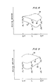
- FIGS. 8 and 9 show the amplitude variations across the signal band for two different fade conditions. If, as illustrated by curve 131 in F I G. 8, the fade notch falls above f c (i.e., between f c and f c + ⁇ f, or above f c + ⁇ f), Ai will typically be much larger than A2 so that the magnitude of Al - A2 will exceed the threshold level V T . If the fade notch falls below f c (i.e., between f c and f c - ⁇ f, or below f c - ⁇ f) as illustrated by curve 132 in F I G. 9, the magnitude of A3-A 2 will exceed V T .
- f c i.e., between f c and f c - ⁇ f, or below f c - ⁇ f
- the output M from gate 117 is level "0", indicating the absence of a multipath fade, or a fade that is shallow enough to be ignored.
- a difference signal is formed in differential amplifier 118 and this difference compared to a zero level reference in comparator 119. If is greater than , as in FIG. 8, a comparator output signal S L of level "1" is produced. If, on the other hand, A 2 1 ⁇ A 2 3 , as in F I G. 9, a comparator output signal SL of level "0" is produced.
- the signal is again sampled at frequencies f c and f c ⁇ f, by means of bandpass filters 36, 37 and 38, and the samples detected in power detectors 120, 121 and 122 to produce signals , and .
- the object here is to examine these three signal components and to determine whether the signal has been undercompensated or overcompensated.
- the equalizer output signal will be substantially flat across the band. If, however, the signal is undercompensated, it will have an amplitude distribution as indicated by curve 133 in FIG. 8. If it is overcompensated, it will have the shape given by curve 134. Accordingly, to determine the output signal state, the midband signal B2is compared with the edgeband signal, farthest from the fade notch.
- B2 is compared with Bi.
- the difference between signals and is formed in a differential amplifier 123 and the resulting difference signal is compared to a zero level reference in a zero level comparator 125.
- the comparator output signal ⁇ 1 is level "0", indicating undercompensation, in which case the gain factors, a i , of the variable attenuators are increased for the minimum phase case, whereas the gain factors, b i , are increased for the nonminimum phase case.
- ⁇ 1 "1" in which case a i is decreased for the minimum phase case, and b i decreased for the nonminimum phase case.
- the actual adjustments of the equalizer parameters are under the control of a microprocessor, such as the BE LL MAC 8 (BELLMAC is a registered trademark of Western Electric Company, Incorporated) microprocessor, or its equivalent.
- a microprocessor such as the BE LL MAC 8 (BELLMAC is a registered trademark of Western Electric Company, Incorporated) microprocessor, or its equivalent.
- FIGS. 10 and 11 outline the above-described procedure for adjusting the equalizer gain parameters a i and b i .
- the microprocessor then reads the control signals M, SL, ⁇ 1 , ⁇ 2 , f n , and P whose meanings are summarized hereinbelow.
- M 1, indicating the presence of a multipath fade
- M 1, indicating the presence of a multipath fade
- the location of the fade is examined by calculating f c - f n . If this value is greater than one-half the channel bandwidth, the fade is out of band. For this case, the nature of the fade (i. e., minimum or nonminimum phase) is irrelevant so that the P setting remains in its previous state.
- the gain factors a i and b i are incremented and/or decremented, depending upon the nature of the fade, as indicated by P.
- FIG. 12 shows an alternative, transversal filter equivalent of the N-stage feed-forward equalizer of F I G. 2.
- This embodiment comprises a delay line 160 with 2 N taps, where the tap spacing is T.
- Each ot the 2 N taps 161-1, 161-2 ... 161-2 N is coupled to a summing network 162 where the 2 N signal components, thus obtained, are summed to produce the equalized output signal.
- the equalizer transfer function H(jw) can be expressed as
- Equation (21) is also the transfer function of a 2 N tap transversal filter with tap spacing T, and tap weights C(-1) i K i for 0 ⁇ i ⁇ 2 N -1.
- the control algorithm described hereinabove with respect to the feed-forward equalizer is equally applicable for controlling a transversal filter equalizer for minimizing linear distortion caused by multipath fading.
- the transversal filter equalizer operates on a modulated carrier signal (either RF or IF), and not on a baseband (i.e., demodulated) signal, which is typically the manner in which conventional transversal filters are used.
Landscapes
- Engineering & Computer Science (AREA)
- Computer Networks & Wireless Communication (AREA)
- Signal Processing (AREA)
- Cable Transmission Systems, Equalization Of Radio And Reduction Of Echo (AREA)
Applications Claiming Priority (2)
| Application Number | Priority Date | Filing Date | Title |
|---|---|---|---|
| US06/293,463 US4415872A (en) | 1981-08-17 | 1981-08-17 | Adaptive equalizer |
| US293463 | 1981-08-17 |
Publications (2)
| Publication Number | Publication Date |
|---|---|
| EP0072542A2 true EP0072542A2 (fr) | 1983-02-23 |
| EP0072542A3 EP0072542A3 (fr) | 1984-07-25 |
Family
ID=23129191
Family Applications (1)
| Application Number | Title | Priority Date | Filing Date |
|---|---|---|---|
| EP82107347A Withdrawn EP0072542A3 (fr) | 1981-08-17 | 1982-08-13 | Egaliseur adaptatif |
Country Status (6)
| Country | Link |
|---|---|
| US (1) | US4415872A (fr) |
| EP (1) | EP0072542A3 (fr) |
| JP (1) | JPS58501300A (fr) |
| CA (1) | CA1178666A (fr) |
| GB (1) | GB2104352B (fr) |
| WO (1) | WO1983000784A1 (fr) |
Cited By (3)
| Publication number | Priority date | Publication date | Assignee | Title |
|---|---|---|---|---|
| GB2187613A (en) * | 1986-03-06 | 1987-09-09 | Gen Electric Plc | Transversal equaliser arrangements |
| EP0325668A1 (fr) * | 1988-01-27 | 1989-08-02 | Blaupunkt-Werke GmbH | Autoradio avec égaliseur non récursif en cascade |
| EP0499227A2 (fr) * | 1991-02-13 | 1992-08-19 | Nec Corporation | Egaliseur adaptif qui exécute une opération d'égalisation avec référence à une magnitude de fading |
Families Citing this family (10)
| Publication number | Priority date | Publication date | Assignee | Title |
|---|---|---|---|---|
| US4547888A (en) * | 1982-07-28 | 1985-10-15 | Motorola, Inc. | Recursive adaptive equalizer for SMSK data links |
| US4538283A (en) * | 1983-07-26 | 1985-08-27 | Rockwell International Corporation | Adaptive equalizer suitable for use with fiber optics |
| NO163120C (no) * | 1987-05-19 | 1990-04-04 | Sintef | Fremgangsmaate ved demodulasjon i digitale kommunikasjonssystemer med flerbane-propagasjon. |
| US5278871A (en) * | 1992-03-19 | 1994-01-11 | Motorola, Inc. | Method and apparatus for estimating signal weighting parameters in a receiver |
| JP3109389B2 (ja) * | 1994-09-30 | 2000-11-13 | アイコム株式会社 | 適応フィルタシステム |
| US5506549A (en) * | 1994-11-14 | 1996-04-09 | Dsc Communications Corporation | Cable equalizer |
| US5940441A (en) * | 1996-10-29 | 1999-08-17 | International Business Machines Corporation | Integrated adaptive cable equalizer using a continuous-time filter |
| GB0026206D0 (en) * | 2000-10-26 | 2000-12-13 | Koninkl Philips Electronics Nv | A method of receiving a signal and a receiver |
| JP4802163B2 (ja) * | 2007-09-03 | 2011-10-26 | 株式会社東芝 | マルチパス等化器を有する受信機及び方法 |
| US11153129B1 (en) * | 2020-06-01 | 2021-10-19 | International Business Machines Corporation | Feedforward equalizer with programmable roaming taps |
Citations (2)
| Publication number | Priority date | Publication date | Assignee | Title |
|---|---|---|---|---|
| US4258340A (en) * | 1978-04-12 | 1981-03-24 | Nippon Electric Co., Ltd. | Amplitude equalizer |
| EP0048646A1 (fr) * | 1980-09-12 | 1982-03-31 | Thomson-Csf | Dispositif de correction des distorsions d'amplitude des signaux radioélectriques, et récepteur comportant un tel dispositif |
Family Cites Families (8)
| Publication number | Priority date | Publication date | Assignee | Title |
|---|---|---|---|---|
| SE375671B (fr) * | 1967-03-16 | 1975-04-21 | Fujitsu Ltd | |
| JPS5334698B1 (fr) * | 1971-06-09 | 1978-09-21 | ||
| GB1490970A (en) * | 1973-12-22 | 1977-11-09 | Dolby Laboratories Inc | Equalizers |
| US3868604A (en) * | 1974-04-08 | 1975-02-25 | Blonder Tongue Lab | Constant resistance adjustable slope equalizer |
| US3947768A (en) * | 1975-01-08 | 1976-03-30 | International Business Machines Corporation | Carrier-modulation data transmission equalizers |
| JPS52153649A (en) * | 1976-06-17 | 1977-12-20 | Kokusai Denshin Denwa Co Ltd | Bessel function automatic delay equalizer |
| FR2374651A1 (fr) * | 1976-12-16 | 1978-07-13 | Labo Cent Telecommunicat | Dispositif d'elimination des lobes secondaires d'auto-correlation d'un signal continu periodique code en phase |
| US4330764A (en) * | 1980-06-11 | 1982-05-18 | Bell Telephone Laboratories, Incorporated | Multipath fade equalizer |
-
1981
- 1981-08-17 US US06/293,463 patent/US4415872A/en not_active Expired - Fee Related
-
1982
- 1982-06-30 CA CA000406374A patent/CA1178666A/fr not_active Expired
- 1982-07-14 WO PCT/US1982/000948 patent/WO1983000784A1/fr unknown
- 1982-07-14 JP JP57502583A patent/JPS58501300A/ja active Granted
- 1982-08-12 GB GB08223248A patent/GB2104352B/en not_active Expired
- 1982-08-13 EP EP82107347A patent/EP0072542A3/fr not_active Withdrawn
Patent Citations (2)
| Publication number | Priority date | Publication date | Assignee | Title |
|---|---|---|---|---|
| US4258340A (en) * | 1978-04-12 | 1981-03-24 | Nippon Electric Co., Ltd. | Amplitude equalizer |
| EP0048646A1 (fr) * | 1980-09-12 | 1982-03-31 | Thomson-Csf | Dispositif de correction des distorsions d'amplitude des signaux radioélectriques, et récepteur comportant un tel dispositif |
Non-Patent Citations (1)
| Title |
|---|
| INTERNATIONAL CONFERENCE ON COMMUNICATIONS, DENVER, COLORADO, CONFERENCE RECORD, vol. 1, 14th-18th June 1981, pages 13.6.1 - 13.6.4, New York (USA); E.R.JOHNSON: "An adaptive IF equalizer for digital transmission * |
Cited By (5)
| Publication number | Priority date | Publication date | Assignee | Title |
|---|---|---|---|---|
| GB2187613A (en) * | 1986-03-06 | 1987-09-09 | Gen Electric Plc | Transversal equaliser arrangements |
| EP0325668A1 (fr) * | 1988-01-27 | 1989-08-02 | Blaupunkt-Werke GmbH | Autoradio avec égaliseur non récursif en cascade |
| WO1989007371A1 (fr) * | 1988-01-27 | 1989-08-10 | Blaupunkt-Werke Gmbh | Circuit correcteur en cascade sous forme non recursive pour eliminer les parasites provoques par une reception sur plusieurs canaux |
| EP0499227A2 (fr) * | 1991-02-13 | 1992-08-19 | Nec Corporation | Egaliseur adaptif qui exécute une opération d'égalisation avec référence à une magnitude de fading |
| EP0499227A3 (en) * | 1991-02-13 | 1992-09-30 | Nec Corporation | Adaptive equalizer which carries out an equalization operation with reference to a magnitude of fading |
Also Published As
| Publication number | Publication date |
|---|---|
| EP0072542A3 (fr) | 1984-07-25 |
| GB2104352A (en) | 1983-03-02 |
| GB2104352B (en) | 1985-04-24 |
| JPH0234488B2 (fr) | 1990-08-03 |
| WO1983000784A1 (fr) | 1983-03-03 |
| US4415872A (en) | 1983-11-15 |
| JPS58501300A (ja) | 1983-08-04 |
| CA1178666A (fr) | 1984-11-27 |
Similar Documents
| Publication | Publication Date | Title |
|---|---|---|
| JP3393650B2 (ja) | 適応型アンプ歪補償回路 | |
| US4415872A (en) | Adaptive equalizer | |
| KR100356250B1 (ko) | 디지탈 상호 변조 제어 기능을 갖는 피드 포워드 앰프 | |
| US4701716A (en) | Parallel distributed signal amplifiers | |
| US6006111A (en) | Self-balancing matrix amplifier | |
| US5789976A (en) | Digital adaptive control of feedforward amplifier using frequency domain cancellation | |
| KR970005293B1 (ko) | 하이 다이나믹 레인지 변조와 무관한 피드 포워드 증폭기 회로망 | |
| US4878030A (en) | Linearizer for microwave amplifier | |
| US5381108A (en) | Automatic calibration of the quadrature balance within a cartesian amplifier | |
| JP4015455B2 (ja) | 歪補償装置 | |
| US7231191B2 (en) | Spurious ratio control circuit for use with feed-forward linear amplifiers | |
| US4003006A (en) | Pilot tone controlled adaptive amplitude equalizer | |
| WO1992019041A1 (fr) | Reseau amplificateur a anticipation avec onde pilote a balayage de frequence | |
| US5062148A (en) | Multi-path fading simulator | |
| JPH10145161A (ja) | プリディストーション自動調整回路 | |
| KR100276403B1 (ko) | 무선 주파수 통신 시스템용 증폭기회로 및 증폭기 제어방법 | |
| JP2003503867A (ja) | 増幅器を直線化する方法及び装置 | |
| US4333063A (en) | Amplitude equalizer | |
| US4330764A (en) | Multipath fade equalizer | |
| US5789993A (en) | Amplitude/frequency correcting device and corresponding frequency equalizer | |
| US4633200A (en) | Voltage controlled equalizer | |
| US4870658A (en) | Amplitude equalizer | |
| US4430744A (en) | Adaptive IF equalizer for digital transmission | |
| JPH06343090A (ja) | Qam型変調を使用するデジタル無線リンクのためのマイクロ波復調器 | |
| US5442328A (en) | Transmission line correction system |
Legal Events
| Date | Code | Title | Description |
|---|---|---|---|
| PUAI | Public reference made under article 153(3) epc to a published international application that has entered the european phase |
Free format text: ORIGINAL CODE: 0009012 |
|
| AK | Designated contracting states |
Designated state(s): CH DE FR IT LI |
|
| PUAL | Search report despatched |
Free format text: ORIGINAL CODE: 0009013 |
|
| AK | Designated contracting states |
Designated state(s): CH DE FR IT LI |
|
| 17P | Request for examination filed |
Effective date: 19840901 |
|
| STAA | Information on the status of an ep patent application or granted ep patent |
Free format text: STATUS: THE APPLICATION IS DEEMED TO BE WITHDRAWN |
|
| 18D | Application deemed to be withdrawn |
Effective date: 19851018 |
|
| RIN1 | Information on inventor provided before grant (corrected) |
Inventor name: KARABINIS, PETER DIMITRIOS |