EP0070858B1 - Current output oscillator - Google Patents
Current output oscillator Download PDFInfo
- Publication number
- EP0070858B1 EP0070858B1 EP82900425A EP82900425A EP0070858B1 EP 0070858 B1 EP0070858 B1 EP 0070858B1 EP 82900425 A EP82900425 A EP 82900425A EP 82900425 A EP82900425 A EP 82900425A EP 0070858 B1 EP0070858 B1 EP 0070858B1
- Authority
- EP
- European Patent Office
- Prior art keywords
- transistor
- current
- coupled
- capacitor
- emitter
- Prior art date
- Legal status (The legal status is an assumption and is not a legal conclusion. Google has not performed a legal analysis and makes no representation as to the accuracy of the status listed.)
- Expired
Links
Images
Classifications
-
- H—ELECTRICITY
- H03—ELECTRONIC CIRCUITRY
- H03K—PULSE TECHNIQUE
- H03K4/00—Generating pulses having essentially a finite slope or stepped portions
- H03K4/06—Generating pulses having essentially a finite slope or stepped portions having triangular shape
- H03K4/08—Generating pulses having essentially a finite slope or stepped portions having triangular shape having sawtooth shape
- H03K4/48—Generating pulses having essentially a finite slope or stepped portions having triangular shape having sawtooth shape using as active elements semiconductor devices
- H03K4/50—Generating pulses having essentially a finite slope or stepped portions having triangular shape having sawtooth shape using as active elements semiconductor devices in which a sawtooth voltage is produced across a capacitor
- H03K4/501—Generating pulses having essentially a finite slope or stepped portions having triangular shape having sawtooth shape using as active elements semiconductor devices in which a sawtooth voltage is produced across a capacitor the starting point of the flyback period being determined by the amplitude of the voltage across the capacitor, e.g. by a comparator
- H03K4/502—Generating pulses having essentially a finite slope or stepped portions having triangular shape having sawtooth shape using as active elements semiconductor devices in which a sawtooth voltage is produced across a capacitor the starting point of the flyback period being determined by the amplitude of the voltage across the capacitor, e.g. by a comparator the capacitor being charged from a constant-current source
-
- H—ELECTRICITY
- H03—ELECTRONIC CIRCUITRY
- H03K—PULSE TECHNIQUE
- H03K3/00—Circuits for generating electric pulses; Monostable, bistable or multistable circuits
- H03K3/02—Generators characterised by the type of circuit or by the means used for producing pulses
- H03K3/023—Generators characterised by the type of circuit or by the means used for producing pulses by the use of differential amplifiers or comparators, with internal or external positive feedback
- H03K3/0231—Astable circuits
Definitions
- This invention relates generally to a current output oscillator circuit and, more particularly, to an integrated circuit current output oscillator which is simple, relatively insensitive to temperature and which occupies a small amount of semiconductor area.
- Relaxation type oscillator circuits which are responsive to voltage trip points and which generate an oscillating output voltage signal are well-known.
- the conventional method of producing an oscillating current is to first generate an oscillating voltage and then perform a voltage-to-current conversion.
- a problem associated with this approach may require excessive semiconductor area and may result in the introduction of additional error during the conversion process.
- a circuit in accordance with the prior art portion of claim 1 is disclosed in EP-A-0013207.
- the present invention provides an improved oscillator circuit in which said second means comprises:
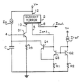
- a first current source I c is coupled between a first voltage terminal (V+) and a first terminal of capacitor C which may be internal or external to the integrated circuit chip.
- the other terminal of capacitor C is coupled to a second voltage supply terminal (e.g. ground).
- a first transistor Q1 has a base coupled to node 4 which is the junction between current source I e and capacitor C and has a collector coupled to the input of current mirror 2.
- the emitter of transistor Q1 is coupled via resistor R3 to the second voltage terminal.
- a second transistor Q2 has its base and collector terminals adapted to receive a reference current I REF .
- the emitter of transistor Q2 is coupled via resistor R2 to the second supply voltage terminal.
- a third transistor Q3 has a base terminal coupled to the base of transistor Q2, an emitter coupled via resistor R1 to the second supply voltage terminal and has a collector coupled to output 6 of current mirror circuit 2.
- a fourth transistor Q4 has at least one emitter coupled to the emitter of transistor Q3, a base coupled to the collector of transistor Q3, and a collector coupled to node 4. The oscillating current output appears at output 8 of current mirror 2. While current mirror 2 is shown only as a block having an input 10, outputs 6 and 8, and a power supply input 12, such circuits are well-known in the art and a further discussion is not deemed necessary.
- the oscillator is of the relaxation type; i.e. the output current rises to a peak level and then is rapidly reset (relaxed) to an initial level.
- current source I c which may be nothing more than a resistor to V+
- I c which may be nothing more than a resistor to V+
- the voltage across capacitor C (and therefore on the base of transistor Q1) begins to rise. This develops a voltage across resistor R3 which in turn causes a collector current to flow in transistor Q1. Since the collector of transistor Q1 is coupled to input 10 of current mirror 2, the current is mirrored to output terminals 6 and 8 of current mirror 2 which correspond to a control current (I CNT ) and the output current of the circuit I OUT respectively.
- I CNT control current
- transistor Q4 When the voltage across capacitor C is sufficient to cause the control current I CNT to exceed the collector current of transistor Q3, transistor Q4 will turn on. Since transistors Q2 and Q3 and resistors R1 and R2 comprise an NPN mirror circuit, Q4 will turn on when the control current I CNT equals the reference current I REF as long as transistor Q2 is identical to transistor Q3 and R1 equals R2. Of course, by varying emitter areas of transistors Q2 and Q3 and by properly scaling the resistor values, the switching point of Q4 could occur when the control current I CNT was in some other way proportionally related to the reference current I REF .
- control current I CNT and the output current will fall as the voltage across the capacitor C is reset since the voltage across resistor R3 is also falling. It is important to note that the peak amplitude of the control current and of the output current is dependent only on the oscillator trip point which is set by the reference current I REF as described above. The peak output current is therefore directly proportional to I REF and is independent of other oscillator components. The temperature coefficient of I OUT(peak) is also directly proportional to the temperature coefficient of I REF .
- Transistor switch Q4 will remain on as long as I CNT provides adequate base current drive to Q4 and the capacitor discharge current through R1 is sufficient to bias transistor Q3 in the off state.
- Output current I OUT , control current I CNT and therefore the base current of transistor Q4 will drop to a very low value when the voltage at the base of transistor Q1 drops to a level which biases Q1 near a turn-off condition; i.e., V BEQ1(loW) ⁇
- the discharge current through R1 decreases to a level which allows transistor Q3 to turn on quickly due to regenerative feedback through transistor Q4. With transistor Q3 on and in saturation, transistor Q4 is again off and the above described cycle will be repeated.
- the peak voltage across capacitor C at the oscillator trip point is equal to the base emitter voltage across transistor Q1 when it is on plus the peak voltage across resistor R3; i.e., V BEQ1(high) +V R3(peak) ⁇
- the capacitor voltage after reset is V BEQ1(loW) .
- the capacitor voltage (V c ) traverses a voltage range equivalent to
Landscapes
- Engineering & Computer Science (AREA)
- Power Engineering (AREA)
- Inductance-Capacitance Distribution Constants And Capacitance-Resistance Oscillators (AREA)
- Dc-Dc Converters (AREA)
- Control Of Electrical Variables (AREA)
- Stabilization Of Oscillater, Synchronisation, Frequency Synthesizers (AREA)
Applications Claiming Priority (2)
| Application Number | Priority Date | Filing Date | Title |
|---|---|---|---|
| US06/229,485 US4336507A (en) | 1981-01-29 | 1981-01-29 | Current output relaxation oscillator |
| US229485 | 2005-09-16 |
Publications (3)
| Publication Number | Publication Date |
|---|---|
| EP0070858A1 EP0070858A1 (en) | 1983-02-09 |
| EP0070858A4 EP0070858A4 (en) | 1984-11-07 |
| EP0070858B1 true EP0070858B1 (en) | 1987-05-06 |
Family
ID=22861437
Family Applications (1)
| Application Number | Title | Priority Date | Filing Date |
|---|---|---|---|
| EP82900425A Expired EP0070858B1 (en) | 1981-01-29 | 1981-12-14 | Current output oscillator |
Country Status (10)
| Country | Link |
|---|---|
| US (1) | US4336507A (enExample) |
| EP (1) | EP0070858B1 (enExample) |
| JP (1) | JPS57502239A (enExample) |
| BR (1) | BR8108957A (enExample) |
| CA (1) | CA1172712A (enExample) |
| DE (1) | DE3176169D1 (enExample) |
| IT (1) | IT1147561B (enExample) |
| MX (1) | MX150525A (enExample) |
| SG (1) | SG42989G (enExample) |
| WO (1) | WO1982002629A1 (enExample) |
Families Citing this family (5)
| Publication number | Priority date | Publication date | Assignee | Title |
|---|---|---|---|---|
| US4418323A (en) * | 1980-03-07 | 1983-11-29 | Pioneer Electronic Corporation | Oscillator having capacitor charged and discharged by current mirror circuits |
| DE3225157A1 (de) * | 1982-07-06 | 1984-01-12 | Robert Bosch Gmbh, 7000 Stuttgart | Regelvorrichtung fuer ein elektrisches stellglied |
| DE3582620D1 (de) * | 1984-07-27 | 1991-05-29 | Omron Tateisi Electronics Co | Einschalt-ruecksetzschaltung fuer einen beruehrungslosen schalter. |
| US4591807A (en) * | 1984-12-03 | 1986-05-27 | Motorola, Inc. | Low power, low voltage oscillator |
| US5379206A (en) * | 1992-12-02 | 1995-01-03 | Argus Technologies, Ltd. | Low loss snubber circuit with active recovery switch |
Family Cites Families (5)
| Publication number | Priority date | Publication date | Assignee | Title |
|---|---|---|---|---|
| US3886485A (en) * | 1972-11-25 | 1975-05-27 | Victor Company Of Japan | Linear voltage controlled oscillator including a timing capacitor charged and discharged through current mirror circuits |
| US3924202A (en) * | 1974-08-21 | 1975-12-02 | Rca Corp | Electronic oscillator |
| FR2445658A1 (fr) * | 1978-12-29 | 1980-07-25 | Thomson Csf | Circuit oscillateur generateur de dents de scie et recepteur de television comportant un tel oscillateur |
| US4263567A (en) * | 1979-05-11 | 1981-04-21 | Rca Corporation | Voltage controlled oscillator |
| US4292604A (en) * | 1979-08-20 | 1981-09-29 | Bell Telephone Laboratories, Incorporated | Relaxation oscillator with plural constant current sources |
-
1981
- 1981-01-29 US US06/229,485 patent/US4336507A/en not_active Expired - Lifetime
- 1981-12-14 JP JP82500454A patent/JPS57502239A/ja active Pending
- 1981-12-14 DE DE8282900425T patent/DE3176169D1/de not_active Expired
- 1981-12-14 WO PCT/US1981/001656 patent/WO1982002629A1/en not_active Ceased
- 1981-12-14 EP EP82900425A patent/EP0070858B1/en not_active Expired
- 1981-12-14 BR BR8108957A patent/BR8108957A/pt unknown
- 1981-12-22 CA CA000392983A patent/CA1172712A/en not_active Expired
-
1982
- 1982-01-08 MX MX190907A patent/MX150525A/es unknown
- 1982-01-08 IT IT47520/82A patent/IT1147561B/it active
-
1989
- 1989-07-17 SG SG42989A patent/SG42989G/en unknown
Also Published As
| Publication number | Publication date |
|---|---|
| JPS57502239A (enExample) | 1982-12-16 |
| BR8108957A (pt) | 1983-01-25 |
| CA1172712A (en) | 1984-08-14 |
| US4336507A (en) | 1982-06-22 |
| DE3176169D1 (en) | 1987-06-11 |
| SG42989G (en) | 1989-12-22 |
| IT8247520A0 (it) | 1982-01-08 |
| WO1982002629A1 (en) | 1982-08-05 |
| MX150525A (es) | 1984-05-18 |
| EP0070858A4 (en) | 1984-11-07 |
| IT1147561B (it) | 1986-11-19 |
| EP0070858A1 (en) | 1983-02-09 |
Similar Documents
| Publication | Publication Date | Title |
|---|---|---|
| US4864213A (en) | DC supply having low and high constant voltages for powering a polarity inverter controller | |
| US4434408A (en) | Oscillator having capacitor charging and discharging controlled by non-saturating switches | |
| US4977381A (en) | Differential relaxation oscillator | |
| EP0317150B1 (en) | Voltage controlled oscillator | |
| EP0070858B1 (en) | Current output oscillator | |
| US4658205A (en) | Reference voltage generating circuit | |
| US4119904A (en) | Low battery voltage detector | |
| KR960016010B1 (ko) | 지연-펄스 발생기 | |
| EP0647019B1 (en) | Circuit for limiting the maximum current value supplied to a load by a power MOS | |
| HK75989A (en) | Current output oscillator | |
| US4418323A (en) | Oscillator having capacitor charged and discharged by current mirror circuits | |
| US4015218A (en) | Temperature compensated solid-state oscillator | |
| US4377790A (en) | Precision differential relaxation oscillator circuit | |
| US4071832A (en) | Current controlled oscillator | |
| US3178609A (en) | Stabilized two-transistor flasher circuit | |
| US4494088A (en) | Oscillator with capacitor charged and discharged by current proportional to a reference current | |
| KR890016571A (ko) | 차아지업 및 디스차아지업 회로를 이용한 기준전압 발생회로 | |
| US3614664A (en) | Class c bridge oscillator | |
| US4223280A (en) | Relaxation oscillator including an SCR and having switch means for interrupting current flow therethrough | |
| US4580069A (en) | Comparator | |
| US4642579A (en) | IC low-capacitance, low-frequency, low-current, non-radiating oscillator | |
| KR930008429B1 (ko) | 가변 주파수 전압제어 발진회로 | |
| US4757280A (en) | NPN transistor RC oscillator | |
| US2986657A (en) | Pulse generator | |
| JP2623739B2 (ja) | 鋸歯状発振回路 |
Legal Events
| Date | Code | Title | Description |
|---|---|---|---|
| PUAI | Public reference made under article 153(3) epc to a published international application that has entered the european phase |
Free format text: ORIGINAL CODE: 0009012 |
|
| 17P | Request for examination filed |
Effective date: 19821011 |
|
| AK | Designated contracting states |
Designated state(s): DE FR GB SE |
|
| GRAA | (expected) grant |
Free format text: ORIGINAL CODE: 0009210 |
|
| AK | Designated contracting states |
Kind code of ref document: B1 Designated state(s): DE FR GB SE |
|
| REF | Corresponds to: |
Ref document number: 3176169 Country of ref document: DE Date of ref document: 19870611 |
|
| ET | Fr: translation filed | ||
| PG25 | Lapsed in a contracting state [announced via postgrant information from national office to epo] |
Ref country code: SE Effective date: 19871215 |
|
| PLBE | No opposition filed within time limit |
Free format text: ORIGINAL CODE: 0009261 |
|
| STAA | Information on the status of an ep patent application or granted ep patent |
Free format text: STATUS: NO OPPOSITION FILED WITHIN TIME LIMIT |
|
| 26N | No opposition filed | ||
| EUG | Se: european patent has lapsed |
Ref document number: 82900425.8 Effective date: 19880913 |
|
| PGFP | Annual fee paid to national office [announced via postgrant information from national office to epo] |
Ref country code: GB Payment date: 19970930 Year of fee payment: 17 |
|
| PGFP | Annual fee paid to national office [announced via postgrant information from national office to epo] |
Ref country code: FR Payment date: 19971015 Year of fee payment: 17 |
|
| PGFP | Annual fee paid to national office [announced via postgrant information from national office to epo] |
Ref country code: DE Payment date: 19971023 Year of fee payment: 17 |
|
| PG25 | Lapsed in a contracting state [announced via postgrant information from national office to epo] |
Ref country code: GB Free format text: LAPSE BECAUSE OF NON-PAYMENT OF DUE FEES Effective date: 19981214 |
|
| GBPC | Gb: european patent ceased through non-payment of renewal fee |
Effective date: 19981214 |
|
| PG25 | Lapsed in a contracting state [announced via postgrant information from national office to epo] |
Ref country code: FR Free format text: LAPSE BECAUSE OF NON-PAYMENT OF DUE FEES Effective date: 19990831 |
|
| REG | Reference to a national code |
Ref country code: FR Ref legal event code: ST |
|
| PG25 | Lapsed in a contracting state [announced via postgrant information from national office to epo] |
Ref country code: DE Free format text: LAPSE BECAUSE OF NON-PAYMENT OF DUE FEES Effective date: 19991001 |