EP0068970B1 - Dispositif stabilisé d'asservissement par tout ou rien à période constante, et dispositif d'alimentation électrique comportant un tel dispositif d'asservissement - Google Patents
Dispositif stabilisé d'asservissement par tout ou rien à période constante, et dispositif d'alimentation électrique comportant un tel dispositif d'asservissement Download PDFInfo
- Publication number
- EP0068970B1 EP0068970B1 EP82401087A EP82401087A EP0068970B1 EP 0068970 B1 EP0068970 B1 EP 0068970B1 EP 82401087 A EP82401087 A EP 82401087A EP 82401087 A EP82401087 A EP 82401087A EP 0068970 B1 EP0068970 B1 EP 0068970B1
- Authority
- EP
- European Patent Office
- Prior art keywords
- signal
- sawtooth
- pulses
- period
- constant
- Prior art date
- Legal status (The legal status is an assumption and is not a legal conclusion. Google has not performed a legal analysis and makes no representation as to the accuracy of the status listed.)
- Expired
Links
- 230000001105 regulatory effect Effects 0.000 claims description 11
- 230000033228 biological regulation Effects 0.000 claims description 7
- 238000004804 winding Methods 0.000 claims 3
- 238000010586 diagram Methods 0.000 description 9
- 230000001276 controlling effect Effects 0.000 description 3
- 238000001914 filtration Methods 0.000 description 3
- 230000000630 rising effect Effects 0.000 description 2
- 230000001360 synchronised effect Effects 0.000 description 2
- 238000005513 bias potential Methods 0.000 description 1
- 239000003990 capacitor Substances 0.000 description 1
- 238000010276 construction Methods 0.000 description 1
- 230000007423 decrease Effects 0.000 description 1
- 230000000694 effects Effects 0.000 description 1
- 238000004519 manufacturing process Methods 0.000 description 1
- 230000003071 parasitic effect Effects 0.000 description 1
- 238000005070 sampling Methods 0.000 description 1
- 230000006641 stabilisation Effects 0.000 description 1
- 238000011105 stabilization Methods 0.000 description 1
Images


Classifications
-
- H—ELECTRICITY
- H02—GENERATION; CONVERSION OR DISTRIBUTION OF ELECTRIC POWER
- H02M—APPARATUS FOR CONVERSION BETWEEN AC AND AC, BETWEEN AC AND DC, OR BETWEEN DC AND DC, AND FOR USE WITH MAINS OR SIMILAR POWER SUPPLY SYSTEMS; CONVERSION OF DC OR AC INPUT POWER INTO SURGE OUTPUT POWER; CONTROL OR REGULATION THEREOF
- H02M3/00—Conversion of DC power input into DC power output
- H02M3/22—Conversion of DC power input into DC power output with intermediate conversion into AC
- H02M3/24—Conversion of DC power input into DC power output with intermediate conversion into AC by static converters
- H02M3/28—Conversion of DC power input into DC power output with intermediate conversion into AC by static converters using discharge tubes with control electrode or semiconductor devices with control electrode to produce the intermediate AC
- H02M3/325—Conversion of DC power input into DC power output with intermediate conversion into AC by static converters using discharge tubes with control electrode or semiconductor devices with control electrode to produce the intermediate AC using devices of a triode or a transistor type requiring continuous application of a control signal
- H02M3/335—Conversion of DC power input into DC power output with intermediate conversion into AC by static converters using discharge tubes with control electrode or semiconductor devices with control electrode to produce the intermediate AC using devices of a triode or a transistor type requiring continuous application of a control signal using semiconductor devices only
- H02M3/33507—Conversion of DC power input into DC power output with intermediate conversion into AC by static converters using discharge tubes with control electrode or semiconductor devices with control electrode to produce the intermediate AC using devices of a triode or a transistor type requiring continuous application of a control signal using semiconductor devices only with automatic control of the output voltage or current, e.g. flyback converters
Definitions
- the present invention relates to a device ensuring a servo stabilized by all or nothing, at constant period, and more precisely the stabilization of the servo of a continuous function, controlled by an all or nothing signal, of constant period.
- a device is particularly applicable to an electrical supply.
- the present invention relates to a servo device which is both stable and suitable for placing modules constituting a supply device in parallel.
- FIG. 1 there is shown a comparator 1 receiving on the one hand a signal 1 to be regulated and on the other hand a servo signal S A ; comparator 1 supplies a signal H ,, consisting of a series of pulses corresponding to the instants when the value of signal I reaches that of signal SA.
- the signal H is directed on the one hand to a bistable circuit 2 (reset reset input) and on the other hand to a sawtooth generator 3.
- the bistable circuit 2 receives on the one hand a signal of clock H o of period T o and on the other hand the signal H, which causes its reset to zero; it outputs a signal S s for controlling the signal 1 to be controlled, which is a signal in time slots of pseudo period T o , the duration ( ⁇ ) of the time slots being determined by the signal H I.
- the sawtooth generator 3 produces a signal S D , which is a sawtooth signal of constant slope but whose period is determined by the signal H I : each of the pulses constituting the signal H, triggers the rising edge of a sawtooth.
- This generator 3 can be produced for example using an integrator, receiving a constant physical quantity G, such as current or voltage, and integrating this quantity between two pulses of the signal H,; such an embodiment is described in FIG. 3.
- the sawtooth signal S D is not directly compared to the signal to be regulated I but it is added to it, via an adder 4, a constant quantity which is a setpoint signal, noted ⁇ , to constitute the signal S A.
- ⁇ a setpoint signal
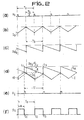
- FIG. 1 The operation of the device of FIG. 1 is explained using diagrams a to f of FIG. 2, representing the evolution as a function of time of different signals likely to exist at different points of this device.
- the first of these diagrams (2a) represents the clock signal H o , which periodically presents (period T o ) pulses in the form of slots.
- T o period of constant period
- the on / off control signal (not shown) is a signal in slots of period T o , the duration of the slots being for example of T o / 2.
- Diagram 2b shows by way of example a signal to be regulated such as a current 1 evolving around an average value according to the state of the control signal described above, denoted I o in the absence of disturbances. It is then a signal of period T o , of constant slope alterna tively positive and negative, the ascent of the signal I o being synchronized with a pulse of the signal H o . It appears that the peak value of this signal is constant.
- Diagram 2c represents the sawtooth signal produced by generator 3, denoted S Do , always in the absence of disturbances. It is a signal of the same period T o as the signal I, of constant slope, whose rising edges are synchronized with the maxima of the signal I and therefore phase-shifted (for example in phase opposition in the example shown ) with respect to the signal H o .
- Diagram 2d represents the slaving by the signal SA of the peak value of a disturbed signal I.
- the signal SA consists of the signal S Do to which the size e.
- the peak value of signal 1 is controlled by the signal SA, that is to say that when the peak of signal I reaches the value of signal S A (instant t 1 on the figure), the slope of the signal I changes direction until the next top of the clock H o (instant t 2 ).
- the signal S A returns to its peak value as shown in the figure and is then distinguished from the previous signal S Do (+ e) in the absence of disturbances.
- the comparator 1 of FIG. 1 delivers a pulse as shown in the diagram 2e, which represents the signal H I , and it is this pulse which, applied to the sawtooth generator 3, allows the signal SA to go back to its peak value.
- Diagram 2f represents the output signal S s of the device, which is a signal in niches of pseudo period T o , this being given by the signal H o , and the duration (denoted 0) of the niches is provided by the signal H I which causes the bistable circuit 2 to reset to zero.
- the device as described in FIGS. 1 and 2 therefore makes it possible to supply a signal S, constituting the control signal for the continuous function I to be controlled.
- This signal S s is an all-or-nothing signal, pseudo-periodic of constant period (T o ) of given amplitude, the only variable of which is its form ratio ⁇ / T.
- FIG. 3 represents an embodiment of the sawtooth generator 3 and of the summator 4 of FIG. 1.
- the generator 3 is an integrator of a physical quantity G, which can for example be a current; it includes a PNP type bipolar transistor 31, connected by its emitter to a bias potential + P 3 , and receiving the quantity G via a resistor 32 on its base.
- the signal H I emanating from the comparator 1 is supplied via a resistor 34 at the base of the transistor 31.
- the collector of this transistor is joined at its base via a capacitor 33. The collector constitutes the integrator output connection 3.
- the summator 4 consists of three resistors 41, 42, 43, before a common point which constitutes the output point of the signal SA intended for the comparator 1.
- the output signal of the integrator 3 is applied to the other terminal of the resistor 41, the signal ⁇ at the other terminal of the resistor 42, and the other terminal of the resistor 43 is connected to ground.
- FIG. 4 represents a second embodiment of the device according to the invention in which we find, connected in a similar manner to what is shown in FIG. 1, the comparator 1, the bistable circuit 2 and the sawtooth generator 3 .
- FIG. 5 represents the detail of the construction of the circuit 3 in the case of FIG. 4.
- FIG. 6 represents an embodiment of an electrical supply device according to the invention, using a servo device as described above in one or the other of its embodiments.
- FIG. 6 shows a filtering device 61, receiving the voltage V E supplied by the network, the object of which is to isolate the input voltage by filtering a certain number of parasitic signals, in particular of transi signals. roofs.
- the voltage VA from the filter 61 is supplied to a converter assembly 5, the function of which is to convert the voltage VA into a signal V B having, after filtering in a filter 62, the characteristics required by the user electronic system; this output signal is noted V s .
- the converter 5 includes the previous servo device, marked 54, which receives the signal after sampling the output voltage V s and comparing it in a comparator 63 to a reference voltage V REF .
- the converter 5 also includes a transformer 51, the primary of which is connected to a bias voltage + P 6 and receives the signal VA, and the secondary of which supplies, via a diode 55, the signal V B. The other end of the secondary is connected to ground.
- the other end of the primary of the transformer 51 is connected to the collector of a bipolar NPN transistor 52 whose emitter is connected to ground via a resistor 53.
- the base of the transistor 52 receives the signal S s supplied by device 54; signal I is supplied to device 54 by the emitter of transistor 52.
Landscapes
- Engineering & Computer Science (AREA)
- Power Engineering (AREA)
- Inverter Devices (AREA)
- Dc-Dc Converters (AREA)
- Feedback Control In General (AREA)
- Electrical Discharge Machining, Electrochemical Machining, And Combined Machining (AREA)
- Control Of Electric Motors In General (AREA)
- Control Of Voltage And Current In General (AREA)
Applications Claiming Priority (2)
| Application Number | Priority Date | Filing Date | Title |
|---|---|---|---|
| FR8111839A FR2507797A1 (fr) | 1981-06-16 | 1981-06-16 | Dispositif stabilise d'asservissement par tout ou rien a periode constante et dispositif d'alimentation electrique comportant un tel dispositif d'asservissement |
| FR8111839 | 1981-06-16 |
Publications (2)
| Publication Number | Publication Date |
|---|---|
| EP0068970A1 EP0068970A1 (fr) | 1983-01-05 |
| EP0068970B1 true EP0068970B1 (fr) | 1985-02-20 |
Family
ID=9259580
Family Applications (1)
| Application Number | Title | Priority Date | Filing Date |
|---|---|---|---|
| EP82401087A Expired EP0068970B1 (fr) | 1981-06-16 | 1982-06-15 | Dispositif stabilisé d'asservissement par tout ou rien à période constante, et dispositif d'alimentation électrique comportant un tel dispositif d'asservissement |
Country Status (6)
| Country | Link |
|---|---|
| US (1) | US4471291A (OSRAM) |
| EP (1) | EP0068970B1 (OSRAM) |
| JP (1) | JPS5851320A (OSRAM) |
| DE (1) | DE3262410D1 (OSRAM) |
| FR (1) | FR2507797A1 (OSRAM) |
| NO (1) | NO158971C (OSRAM) |
Families Citing this family (3)
| Publication number | Priority date | Publication date | Assignee | Title |
|---|---|---|---|---|
| FR2577358B1 (fr) * | 1985-02-08 | 1987-03-06 | Thomson Csf | Alimentation a decoupage protegee contre des surintensites tres fortes |
| US4672518A (en) * | 1986-07-30 | 1987-06-09 | American Telephone And Telegraph Co., At&T Bell Labs | Current mode control arrangement with load dependent ramp signal added to sensed current waveform |
| FR2737342B1 (fr) * | 1995-07-25 | 1997-08-22 | Thomson Csf | Composant semiconducteur avec dissipateur thermique integre |
Family Cites Families (10)
| Publication number | Priority date | Publication date | Assignee | Title |
|---|---|---|---|---|
| US3319151A (en) * | 1963-10-05 | 1967-05-09 | Bbc Brown Boveri & Cie | Control arrangement for self-guided inverters |
| US3323037A (en) * | 1964-05-04 | 1967-05-30 | Avco Corp | Voltage regulator utilizing a controlled variable duty cycle switch |
| BE791943A (fr) * | 1972-02-18 | 1973-03-16 | Telecomunicazioni Soc It | Regulateur de tension et/ou de courant |
| DE2445034A1 (de) * | 1974-09-20 | 1976-04-01 | Siemens Ag | Schaltungsanordnung fuer einen mittelfrequenzumrichter |
| FR2295479A1 (fr) * | 1974-12-20 | 1976-07-16 | Radiotechnique | Circuit de commande pour alimentation regulee a decoupage, notamment pour recepteur de television |
| US4032830A (en) * | 1975-07-03 | 1977-06-28 | Burroughs Corporation | Modular constant current power supply |
| DE2621763A1 (de) * | 1976-05-15 | 1977-11-24 | Olympia Werke Ag | Sperrwandler-netzgeraet |
| DE2716500A1 (de) * | 1977-04-14 | 1978-10-26 | Bosch Gmbh Robert | Spannungsregler fuer eine gleichspannung |
| FR2413710A1 (fr) * | 1977-12-29 | 1979-07-27 | Thomson Csf | Circuit de commande de puissance et alimentation a decoupage l'utilisant |
| NL7803661A (nl) * | 1978-04-06 | 1979-10-09 | Philips Nv | Afgestemde geschakelde voedingsspanningsschakeling. |
-
1981
- 1981-06-16 FR FR8111839A patent/FR2507797A1/fr active Granted
-
1982
- 1982-06-10 US US06/387,236 patent/US4471291A/en not_active Expired - Fee Related
- 1982-06-15 NO NO821987A patent/NO158971C/no unknown
- 1982-06-15 EP EP82401087A patent/EP0068970B1/fr not_active Expired
- 1982-06-15 DE DE8282401087T patent/DE3262410D1/de not_active Expired
- 1982-06-16 JP JP57102316A patent/JPS5851320A/ja active Pending
Also Published As
| Publication number | Publication date |
|---|---|
| JPS5851320A (ja) | 1983-03-26 |
| NO158971C (no) | 1988-11-16 |
| US4471291A (en) | 1984-09-11 |
| NO158971B (no) | 1988-08-08 |
| FR2507797A1 (fr) | 1982-12-17 |
| FR2507797B1 (OSRAM) | 1983-10-07 |
| DE3262410D1 (en) | 1985-03-28 |
| EP0068970A1 (fr) | 1983-01-05 |
| NO821987L (no) | 1982-12-17 |
Similar Documents
| Publication | Publication Date | Title |
|---|---|---|
| EP0018343B1 (fr) | Hacheur de courant pour la régulation de l'alimentation d'une charge | |
| EP0052536B1 (fr) | Dispositif de stabilisation de la puissance de sortie d'un module émetteur pour système de transmission sur fibre optique | |
| FR2634293A2 (fr) | Systeme de regulation du point de fonctionnement d'une alimentation a courant continu en zone de caracteristique generateur de tension ou de courant imposee | |
| EP0190961A1 (fr) | Alimentation en courant continu à point de fonctionnement ajustable | |
| FR2489622A1 (fr) | Alimentation stabilisee a accumulation avec transformateur | |
| EP0804038A3 (en) | Solid-state image sensing device | |
| FR2473239A1 (fr) | Televiseur avec circuit generateur de retard | |
| FR2610149A1 (fr) | Convertisseur continu-continu a rendement eleve a faible charge | |
| FR2473234A1 (fr) | Circuit a impedance electriquement variable et a compensation par reaction | |
| EP0068970B1 (fr) | Dispositif stabilisé d'asservissement par tout ou rien à période constante, et dispositif d'alimentation électrique comportant un tel dispositif d'asservissement | |
| FR2573257A1 (fr) | Circuit de protection contre les coupures d'alimentation electrique | |
| FR2550028A1 (fr) | Circuit d'alimentation delivrant des tensions continues d'egale grandeur mais de polarite opposee, notamment pour appareils de reproduction sonore a bord d'automobiles | |
| FR2679718A1 (fr) | Circuit regulateur de la tension de charge d'une batterie par un alternateur. | |
| FR2701612A1 (fr) | Procédé de commande de la puissance appliquée à un onduleur à résonance. | |
| EP0072593A1 (fr) | Dispositif de verrouillage de phase pour fournir à sa sortie des signaux dont la fréquence peut varier sur une large gamme | |
| FR2486326A1 (fr) | Circuit de commande d'un transistor de commutation dans un convertisseur statique et convertisseur le comportant | |
| FR2490895A1 (fr) | Circuit d'entretien pour oscillateur a faible consommation de courant | |
| EP0305301B1 (fr) | Circuit compresseur de signal, en particulier pour appareil téléphonique | |
| FR2578666A1 (fr) | Circuit de commande a compensation des variations de la tension anodique, pour etage de deviation verticale de televiseur | |
| FR2463541A1 (fr) | Generateur d'impulsions | |
| EP0119927B1 (fr) | Amplificateur haute tension pour charge capacitive | |
| EP0111980A2 (fr) | Procédé et dispositif pour aligner le niveau de noir d'un signal vidéofréquence | |
| FR2802366A1 (fr) | Bascule analogique a commande par impulsions | |
| FR2480527A1 (fr) | Alimentation continue, applicable notamment pour alimenter un tube cathodique | |
| EP0289379B1 (fr) | Capteur de mesure d'une grandeur physique |
Legal Events
| Date | Code | Title | Description |
|---|---|---|---|
| PUAI | Public reference made under article 153(3) epc to a published international application that has entered the european phase |
Free format text: ORIGINAL CODE: 0009012 |
|
| AK | Designated contracting states |
Designated state(s): BE DE GB IT NL SE |
|
| 17P | Request for examination filed |
Effective date: 19830127 |
|
| RBV | Designated contracting states (corrected) |
Designated state(s): DE GB |
|
| GRAA | (expected) grant |
Free format text: ORIGINAL CODE: 0009210 |
|
| AK | Designated contracting states |
Designated state(s): DE GB |
|
| REF | Corresponds to: |
Ref document number: 3262410 Country of ref document: DE Date of ref document: 19850328 |
|
| PLBE | No opposition filed within time limit |
Free format text: ORIGINAL CODE: 0009261 |
|
| STAA | Information on the status of an ep patent application or granted ep patent |
Free format text: STATUS: NO OPPOSITION FILED WITHIN TIME LIMIT |
|
| 26N | No opposition filed | ||
| PGFP | Annual fee paid to national office [announced via postgrant information from national office to epo] |
Ref country code: GB Payment date: 19900518 Year of fee payment: 9 |
|
| PGFP | Annual fee paid to national office [announced via postgrant information from national office to epo] |
Ref country code: DE Payment date: 19900519 Year of fee payment: 9 |
|
| PG25 | Lapsed in a contracting state [announced via postgrant information from national office to epo] |
Ref country code: GB Effective date: 19910615 |
|
| GBPC | Gb: european patent ceased through non-payment of renewal fee | ||
| PG25 | Lapsed in a contracting state [announced via postgrant information from national office to epo] |
Ref country code: DE Effective date: 19920401 |