EP0062100A2 - Thyristor with internal-current amplification, and process for its operation - Google Patents
Thyristor with internal-current amplification, and process for its operation Download PDFInfo
- Publication number
- EP0062100A2 EP0062100A2 EP81108715A EP81108715A EP0062100A2 EP 0062100 A2 EP0062100 A2 EP 0062100A2 EP 81108715 A EP81108715 A EP 81108715A EP 81108715 A EP81108715 A EP 81108715A EP 0062100 A2 EP0062100 A2 EP 0062100A2
- Authority
- EP
- European Patent Office
- Prior art keywords
- emitter
- auxiliary emitter
- base
- thyristor
- semiconductor
- Prior art date
- Legal status (The legal status is an assumption and is not a legal conclusion. Google has not performed a legal analysis and makes no representation as to the accuracy of the status listed.)
- Granted
Links
- 230000003321 amplification Effects 0.000 title claims abstract description 17
- 238000003199 nucleic acid amplification method Methods 0.000 title claims abstract description 17
- 238000000034 method Methods 0.000 title claims description 8
- 239000004065 semiconductor Substances 0.000 claims abstract description 34
- 239000002800 charge carrier Substances 0.000 claims abstract description 4
- 102000004207 Neuropilin-1 Human genes 0.000 claims description 6
- 108090000772 Neuropilin-1 Proteins 0.000 claims description 6
- 230000005669 field effect Effects 0.000 claims description 6
- 230000006798 recombination Effects 0.000 claims description 6
- 238000005215 recombination Methods 0.000 claims description 6
- 102000004213 Neuropilin-2 Human genes 0.000 claims description 4
- 108090000770 Neuropilin-2 Proteins 0.000 claims description 4
- 230000000903 blocking effect Effects 0.000 claims description 4
- 230000035945 sensitivity Effects 0.000 abstract description 9
- 108091006146 Channels Proteins 0.000 description 11
- 230000007547 defect Effects 0.000 description 4
- 230000035515 penetration Effects 0.000 description 4
- 238000009792 diffusion process Methods 0.000 description 3
- 238000002513 implantation Methods 0.000 description 3
- 239000013641 positive control Substances 0.000 description 3
- 238000013459 approach Methods 0.000 description 2
- 239000012535 impurity Substances 0.000 description 2
- BASFCYQUMIYNBI-UHFFFAOYSA-N platinum Chemical compound [Pt] BASFCYQUMIYNBI-UHFFFAOYSA-N 0.000 description 2
- 108010075750 P-Type Calcium Channels Proteins 0.000 description 1
- 239000003795 chemical substances by application Substances 0.000 description 1
- 230000008094 contradictory effect Effects 0.000 description 1
- 238000011161 development Methods 0.000 description 1
- 230000018109 developmental process Effects 0.000 description 1
- 238000010894 electron beam technology Methods 0.000 description 1
- 238000005530 etching Methods 0.000 description 1
- 238000010304 firing Methods 0.000 description 1
- PCHJSUWPFVWCPO-UHFFFAOYSA-N gold Chemical compound [Au] PCHJSUWPFVWCPO-UHFFFAOYSA-N 0.000 description 1
- 239000010931 gold Substances 0.000 description 1
- 229910052737 gold Inorganic materials 0.000 description 1
- 230000001678 irradiating effect Effects 0.000 description 1
- 239000000463 material Substances 0.000 description 1
- 239000013642 negative control Substances 0.000 description 1
- 229910052697 platinum Inorganic materials 0.000 description 1
- 229910021420 polycrystalline silicon Inorganic materials 0.000 description 1
- 229920005591 polysilicon Polymers 0.000 description 1
- 229910052710 silicon Inorganic materials 0.000 description 1
- 239000010703 silicon Substances 0.000 description 1
- 230000007704 transition Effects 0.000 description 1
Images


Classifications
-
- H—ELECTRICITY
- H01—ELECTRIC ELEMENTS
- H01L—SEMICONDUCTOR DEVICES NOT COVERED BY CLASS H10
- H01L29/00—Semiconductor devices adapted for rectifying, amplifying, oscillating or switching, or capacitors or resistors with at least one potential-jump barrier or surface barrier, e.g. PN junction depletion layer or carrier concentration layer; Details of semiconductor bodies or of electrodes thereof ; Multistep manufacturing processes therefor
- H01L29/02—Semiconductor bodies ; Multistep manufacturing processes therefor
- H01L29/06—Semiconductor bodies ; Multistep manufacturing processes therefor characterised by their shape; characterised by the shapes, relative sizes, or dispositions of the semiconductor regions ; characterised by the concentration or distribution of impurities within semiconductor regions
- H01L29/10—Semiconductor bodies ; Multistep manufacturing processes therefor characterised by their shape; characterised by the shapes, relative sizes, or dispositions of the semiconductor regions ; characterised by the concentration or distribution of impurities within semiconductor regions with semiconductor regions connected to an electrode not carrying current to be rectified, amplified or switched and such electrode being part of a semiconductor device which comprises three or more electrodes
- H01L29/1012—Base regions of thyristors
- H01L29/102—Cathode base regions of thyristors
-
- H—ELECTRICITY
- H01—ELECTRIC ELEMENTS
- H01L—SEMICONDUCTOR DEVICES NOT COVERED BY CLASS H10
- H01L29/00—Semiconductor devices adapted for rectifying, amplifying, oscillating or switching, or capacitors or resistors with at least one potential-jump barrier or surface barrier, e.g. PN junction depletion layer or carrier concentration layer; Details of semiconductor bodies or of electrodes thereof ; Multistep manufacturing processes therefor
- H01L29/66—Types of semiconductor device ; Multistep manufacturing processes therefor
- H01L29/68—Types of semiconductor device ; Multistep manufacturing processes therefor controllable by only the electric current supplied, or only the electric potential applied, to an electrode which does not carry the current to be rectified, amplified or switched
- H01L29/70—Bipolar devices
- H01L29/74—Thyristor-type devices, e.g. having four-zone regenerative action
- H01L29/7404—Thyristor-type devices, e.g. having four-zone regenerative action structurally associated with at least one other device
- H01L29/742—Thyristor-type devices, e.g. having four-zone regenerative action structurally associated with at least one other device the device being a field effect transistor
-
- H—ELECTRICITY
- H01—ELECTRIC ELEMENTS
- H01L—SEMICONDUCTOR DEVICES NOT COVERED BY CLASS H10
- H01L29/00—Semiconductor devices adapted for rectifying, amplifying, oscillating or switching, or capacitors or resistors with at least one potential-jump barrier or surface barrier, e.g. PN junction depletion layer or carrier concentration layer; Details of semiconductor bodies or of electrodes thereof ; Multistep manufacturing processes therefor
- H01L29/66—Types of semiconductor device ; Multistep manufacturing processes therefor
- H01L29/68—Types of semiconductor device ; Multistep manufacturing processes therefor controllable by only the electric current supplied, or only the electric potential applied, to an electrode which does not carry the current to be rectified, amplified or switched
- H01L29/70—Bipolar devices
- H01L29/74—Thyristor-type devices, e.g. having four-zone regenerative action
- H01L29/7428—Thyristor-type devices, e.g. having four-zone regenerative action having an amplifying gate structure, e.g. cascade (Darlington) configuration
Definitions
- the invention relates to a thyristor with internal current amplification according to the preamble of claim 1 and to methods for its operation.
- a thyristor of this type is known from the "Thyristor Manual" by A. Hoffmann and K. Stokker, Verlag Siemens AG, Berlin and Kunststoff, 1965, pages 27 and 28.
- a current flows through the auxiliary emitter, which is referred to there as an intermediate grid, which causes rapid and large-scale firing in the area of the main emitter.
- a thyristor of this type is suitable for high rates of rise in the load current flowing between the anode and cathode, i.e. H. it has a high di / dt strength.
- German patent application P 29 45 347.2 describes a thyristor with internal current amplification, in which the main emitter has a plurality of fixed emitter short circuits, while the auxiliary emitter is provided with emitter short circuits, which can optionally be switched effectively by means of FET structures, i.e. H. are controllable. If they are activated, the thyristor has good stability, i. H. a high level of security against unintentional ignition processes when forward polarized voltages occur, which under certain circumstances can increase very quickly, i. H. represent a high dU / dt load. On the other hand, the thyristor is sensitive to ignition when the short circuits are ineffective.
- the advantage that can be achieved with the invention is in particular that the switchable auxiliary emitter is ineffective on the one hand in the non-conductive state of the semiconductor switch and does not reduce the stability of the thyristor, while on the other hand it significantly increases the ignition sensitivity of the thyristor in the conductive state of the semiconductor switch.
- the ignition sensitivity increases to the extent that the current amplification factor of the structure, which comprises the connectable auxiliary emitter and the two base layers, is greater with respect to the charge carriers emitted by the connectable auxiliary emitter than the corresponding current amplification factor of the structure, which comprises the auxiliary emitter and the two base layers .
- Claims 2 to 11 are directed to preferred refinements and developments of the invention, while claims 12 and 13 indicate advantageous methods for operating the thyristor according to the invention.
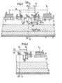
- a thyristor is shown, the one made of doped semiconductor material, for. B. silicon, existing semiconductor body with four layers of alternating conductivity types.
- the n-type layer 1 is referred to as the n-emitter, the p-type layer 2 as the p-base, the n-type layer 3 as the n-base and the p-type layer 4 as the p-type emitter .
- the p-emitter 4 is provided with an anode 5, which has a connection A, while the n-emitter 1 has a cathode 6 with a connection K.
- the n-emitter 1, ' which is the main emitter is penetrated by a plurality of lugs 7 of the p-base 2, extending up to the interface 8 of the semiconductor body and are conductively connected to the cathode in this. 6
- the approaches 7 represent so-called fixed emitter short circuits, which largely prevent an unintentional ignition of the thyristor when a blocking voltage is applied to the connections A and K, which places the anode 5 at a more positive potential than the cathode 6. This is explained by the fact that the defect electrons transported under the influence of the blocking voltage in the direction of the n-emitter 1 largely do not lead to the pn junction between parts 1 and.
- the thyristor is also insensitive to ignition, ie stable, with respect to larger or rapidly increasing blocking voltages at the connections A, K.
- n-type region 9, which represents the auxiliary emitter is inserted into the p-base 2 so that it extends to the interface 8.
- an auxiliary emitter electrode 10 contacts it, which conductively bridges the pn junction between the region 9 and the p base 2 in the direction of the n emitter 1.
- n-type region 11 extends starting from from the interface 8, much deeper into the P base 2 than the n-emitter 1 and the auxiliary emitter 9 and is produced by diffusion or implantation and subsequent driving of donors into the p-base 2. It is arranged laterally next to the auxiliary emitter 9, there being a distance from this which is determined by the width of a region 12 of the p-base 2.
- the area 12 is covered by a metallic or polysilicon gate 13 which is covered by a thin, electrically insulating layer 14, e.g. B. Si0 21 is separated from the interface 8.
- the gate 13 is connected to a control voltage socket 15.
- the mutually facing edge regions of the auxiliary emitter 9 and the region 11 together with the region 12, the insulating layer 14 and the gate 13 form a field effect transistor of the enhancement type.
- a control voltage which is positive in relation to K and exceeds the value of the threshold voltage is applied to the connection 15, an inversion channel is formed at the interface 8 below 13, which is indicated by 16.
- This n-conducting channel represents a low-resistance connection between regions 9 and 11. If the control voltage from terminal 15 is switched off, channel 16 is eliminated and the connection between regions 9 and 11 is interrupted.
- the structure formed from parts 9 to 16 thus represents a semiconductor switch which, in a first switching state, connects region 11 with low resistance to auxiliary emitter 9, so that an enlarged auxiliary emitter 9, 11 is formed, while in a second switching state, region 11 of isolates the auxiliary emitter 9 so that 11 cannot perform an auxiliary emitter function.
- area 11 is referred to as a switchable auxiliary emitter.
- the depth of penetration of the switchable express emitter 11 into the p-base 2 in the embodiment shown in FIG. 1 is more than twice the penetration depth of the express emitter 9 or that of the n-emitter 1. If one assumes a penetration depth of approximately 20 ⁇ m for the auxiliary emitter 9, the penetration depth of 11 is, for example, 50 ⁇ m. Accordingly, the distance D1 of the switchable auxiliary emitter 11 from the pn junction between the base layers 2 and 3 is smaller than the distance D2 of the auxiliary emitter 9 or the n-emitter 1 from this transition.
- the ignition of the thyristor according to FIG. 1 is explained below. It is assumed that a voltage that poles the thyristor in the forward direction is present at connections A and K and that a positive control voltage is supplied to connection 15. Under the influence of the first-mentioned voltage, for example, thermally generated defect electrons move along the path 1-7 shown in FIG. 1 in the direction of a fixed emitter short circuit 7, so that a voltage drop occurs at conductive channel 16 at point 18, which causes the pn junction between the connected auxiliary emitter 11 and the p-base 2 so far in the forward direction that electrons are emitted into the p-base 2 at this point.
- the electrons emitted by 11 move in the direction of the arrow 19, some of them the interface between reached the n-base 3 and the p-emitter 4 and caused an emission of defect electrons from the p-emitter. These emission processes mutually increase until layers 2 and 3 are flooded with emitted charge carriers, i. H. the thyristor has ignited in the area of the switchable auxiliary emitter 11.
- the load current flowing from A via the auxiliary emitter 9, 11 and the auxiliary emitter electrode 10 to the n-emitter 1 and to the cathode 6 represents a large ignition current for the n-emitter 1.
- the load current flowing between A and K becomes completely taken over by the part of the thyristor cross section which contains the ignited part of the n-emitter 1.
- the auxiliary emitter 9 is then no longer flowed through by the load current.
- a pulse-shaped control voltage P1 can thus be supplied to the connection 15, which is switched off when the thyristor cross section has become live in the area of the n-emitter 1.
- the thyristor is fired at lower voltages between A and K than was assumed in the above considerations, by means of an ignition current pulse P2, which is connected to an ignition circuit connected to 21 is fed.
- the bias voltage at the circuit point 18 is generated here by defect electrons which come from the semiconductor region below the ignition electrode 20 and reach a fixed short circuit 7 via the paths 17a and 17 shown in FIG. 1.
- the terminal 15 is connected to the control voltage P1 at the same time. Conveniently, the terminals 15 and 21 connected to each other, wherein the ignition current pulse P2 from the terminal 15 the voltage pulse P1 - drops.
- the thyristor is extinguished when the load current falls below a so-called holding current. This happens, for example, when the voltage from terminals A and K is switched off, or, if it is an AC voltage, when the next zero crossing occurs.
- the current amplification factor ⁇ npn1 of the npn structure formed from parts 11, 2 and 3, which refers to the electrons emitted by 11 is significantly larger than the current amplification factor ⁇ npn2 for the npn structure formed from parts 9, 2 and 3. This can be explained from the fact that the recombination rate of the electrons emitted by 9 is substantially greater than the recombination rate of the electrons emitted by 11 because of the greater distance D2 of the auxiliary emitter 9 from the interface between 2 and 3.
- the ignition sensitivity of the thyristor according to FIG. 1 is therefore greater than the ignition sensitivity of a conventional thyristor with internal ignition amplification, as the current amplification factor ⁇ npn1 is greater than ⁇ npn2 .
- the p-base 2 has a doping profile in which the degree of doping in the region of the lower boundary surface of the switchable auxiliary emitter 11 is smaller than on the lower boundary surface of the auxiliary emitter 9, then the prestress of the pn junction between the semiconductor parts 11 prevailing at point 18 becomes and 2 compared to the case in which the degree of doping of the p base does not have such a reduction, so that the ignition sensitivity in the region of the switchable auxiliary emitter 11 increases further.
- FIG. 1 If one now starts in FIG. 1 from a rotationally symmetrical structure of the thyristor with the line 22 as an axis of symmetry, there are annular configurations of parts 1, 9, 11, 6, 10 and 13. The sectional areas of these parts which are to the left of 22 , are designated 1 ', 9', 11 ', 6', 10 'and 13'. Such a structure is ignited along a circle concentric to axis 22, which contains points 18 and 18 '.
- line 22 in FIG. 1 can also be drawn up as a plane of symmetry perpendicular to the image plane be caught.
- the parts 1, 9, 11; 6, 10 and 13 expediently have an elongated shape and, with their larger dimensions, run perpendicular to the plane of the drawing, preferably over the entire thyristor cross section.
- Parts 1 ', 9', 11 ', 6', 10 'and 13' then represent analog partial structures on the other side of the plane of symmetry, which are symmetrical with respect to the latter with respect to parts 1, 9, 11, 6, 10 and 13 lie.
- the gates 13 and 13 ' are connected to one another for the purpose of a common control, which is indicated by a line 23 shown in the drawing, and can be connected to the connection 21.
- the cathode 6 ' is connected to the cathode 6, which is indicated by a line 24.
- the parts 1, 9, 11, 6, 10 and 13 can advantageously also be strip-shaped and cover the thyristor cross section or parts thereof in the form of a spiral or the like.
- a switchable auxiliary emitter 25 is provided which takes the place of the switchable auxiliary emitter 11 of FIG. 1 and has the same external dimensions as the p base 2 as this. It is provided on the edge zones of a trench-shaped recess 26 of the p-base 2, with it starting from the edge of the same only a few ⁇ m, for. B. 5 microns, extends deep into the p-base 2.
- the n-type region 25 is produced by diffusion or implantation of donors, while the recess 26 is preferably produced by etching.
- the other circuit parts of FIG. 2 correspond to the same-named circuit parts of FIG. 1.
- FIG. 3 shows a thyristor with a p-emitter 27, an n-base 28 and a p-base 29.
- An auxiliary emitter 30 and a switchable auxiliary emitter 31 replace parts 9 and 11 of FIG. 1 and have the same lateral dimensions compared to that p-base 29 on parts 9 and 11 with respect to p-base 2.
- 32 denotes an n-emitter, which takes the place of the n-emitter 1 from FIG. 1 and has the same lateral dimensions as this.
- the vertical dimensions of the parts 30 to 32 are matched to one another, wherein they are expediently larger than the vertical dimension of the n-emitter 1 and, for example, correspond to those of the parts 11 and 11 'in FIG. 1.
- the other circuit parts of FIG. 3 correspond to the circuit parts of FIG. 1 provided with the same reference symbols.
- the n-emitter 32 and the auxiliary emitter 30 are surrounded by a partial region 33 of the p-base 29, which has an additional p-doping, so that its degree of doping is higher than that of the remaining partial regions of the p-base 29.
- the three-layer structure consisting of parts 30, 29 and 28 has a current amplification factor a n p n2 with respect to the electrons emitted in the case of a voltage of 30 at A and K in the forward direction of the thyristor, which is smaller than the corresponding one Current amplification factor a n p n1 of the three-layer structure 31, 29 and 28 with respect to the electrons emitted by the switchable auxiliary emitter 31.
- the terminal 15 is a control voltage, for. B. P1, which causes regions 30 and 31 to be connected to each other in a low-resistance manner via the inversion channel indicated by 16, the thyristor in region 31 is very sensitive to ignition.
- the control voltage from terminal 15 is switched off, the auxiliary emitter 31 is ineffective, so that the thyristor has great stability because of the fixed emitter short circuits 7 and the high doping of the partial region 33.
- an impurity concentration in the p-base 29 of approximately 5 ⁇ 10 16 cm -3
- an impurity concentration occurs for the partial region 33, for example Concentration of about 2 x 10 17 cm -3 into consideration, these figures only serve to explain the doping difference mentioned and are not to be interpreted as limit values.
- Different current amplification factors ⁇ npn1 and a n p n2 can also be achieved in such a way that the partial region 33 is not more heavily doped than the other parts of the p-emitter 29, but instead is provided with additional recombination centers. This happens e.g. B. by irradiating the p-base 29 to the partial region 33 before generating the regions 32 and 30 with an electron beam.
- recombination centers in the form of gold or platinum antibodies can also be introduced into the partial region 33 by diffusion or implantation. The increase in the number of recombination centers in partial area 33 results in a decrease in ⁇ npn2 compared to ⁇ npn1 .
- the thyristors according to FIGS. 2 and 3 are operated in the same way as the thyristor according to FIG. 1.
- the exemplary embodiment shown in FIG. 4 differs from FIG. 1 in that 7 controllable emitter short-circuits are provided instead of the fixed emitter short-circuits.
- the n-emitter 1 of FIG. 1 is divided into two or more emitter subregions 1a, 1b, each of which is provided with a part 6a or 6b of the cathode.
- the parts 6a and 6b are connected to one another and led to a common connection K.
- a controllable emitter short circuit designated SE 1 in FIG. 4, has a p-type semiconductor region 34 inserted into the emitter sub-region 1 a, which extends to the interface 8 of the semiconductor body and in which the part 6 a of the cathode contacts it.
- the emitter subregions 1a and 1b are through a region 35 the p base 2 separated from one another, which is to be understood as a second p-type semiconductor region of the controllable emitter short circuit.
- the latter is covered by a gate 37, which has a connection 38 and a thin, electrically insulating layer 39, for. B.
- the parts 34 to 37 form a FET structure of the depletion type, in which, without supplying a control voltage to the connection 38, there is a p-type channel 40 in the edge region 36 which defines the region 34 with the region 35 and thus the part 6a of the cathode connects to the p-base 2 with low resistance.
- the channel 40 is either an inversion channel or a doped channel generated by a p-doping at the interface 8.
- the emitter short-circuit SE1 is thus effectively switched when the connection 38 is voltage-free. If the connection 38 is supplied with a positive control voltage, the channel 40 is eliminated and the low-resistance connection of parts 2 and 6a is interrupted, ie the emitter short circuit SE1 is deactivated.
- FIG. 4 a further controllable emitter short-circuit SE2 is provided at the edge of the emitter sub-region 1b, which is constructed in accordance with SE1.
- the gate 37 is assigned to the emitter short circuits SE1 and SE2 together.
- a line designated 41 which connects the connections 38 and 15 to one another, is expediently provided.
- the connections 15 and 38 can also be connected individually or together to the connection 21.
- the other circuit parts in FIG. 4 correspond to the parts in FIG. 1 which have the same reference numerals
- E m itter subareas 1a and 1b can, in the embodiment of FIG. 4 also several correspondingly shaped emitter sub-regions, or even a single such sub-region, for. B. 1a or 1b.
- a particularly high stability is achieved with the exemplary embodiment according to FIG. 4, in particular when a larger number of emitter sub-regions 1a, 1b ... and a correspondingly large number of controllable emitter short-circuits SE1, SE2 ... are provided. These are caused by a positive control voltage, e.g. B. pulse-shaped control voltage P3, ineffective so that the spread of the ignited front is not hindered by the emitter short circuits over the entire thyristor cross section. If the thyristor cross in the area of E m itter subareas 1a, 1b become energized, the control voltage can be switched off, as indicated by P3. If a connection 21 is provided, to which an ignition current pulse P2 is supplied, connection 38 can be connected to 21 in order to be able to use the voltage dropping at 21 as control voltage P3. The connection 15 is controlled in the manner already shown in FIG. -1 explained way.
- the FET structures described so far, e.g. 34 to 40 of the depletion type can also be replaced by FET structures of the enhancement type if their gate connections, e.g. B. 38, an additional negative control voltage is supplied, the I n version channels, z. B. 40, arises.
- the control voltage P3 is then superimposed on this additional control voltage at the ignition point in order to cancel the channels.
- FIG. 5 shows another embodiment of the exemplary embodiment according to FIG. 1, in which the connectable auxiliary emitter 11 is conductively connected to the auxiliary emitter 9 via a semiconductor switch in the form of an external field effect transistor 42.
- the source-drain path of 42 is connected on the one hand to the auxiliary emitter electrode 10 and on the other hand to a conductive assignment 43, which contacts the switchable auxiliary emitter 11.
- the gate of 42 is provided with a control voltage connection 44 which can be connected to the connection 21 via a line 45.
- the operation of the thyristor according to FIG. 5 takes place in the manner described with reference to FIG. 1, the connection 44 corresponding to the connection 15 and being supplied with the control voltage P1, while an ignition current pulse P2 is optionally supplied to the connection 21.
- the switchable auxiliary emitter can also be p-conducting, arranged laterally next to the p-emitter in the n-base of the thyristor and connected to this p-emitter with a low resistance to produce a high ignition sensitivity via a semiconductor switch.
- the fixed or controllable emitter short-circuits are also provided in the area of the p-emitter. All of the figures can be used to illustrate this circuit variant if the names of the connections A and K are interchanged, the semiconductor parts each receive the opposite line types to those described so far, and the control voltages mentioned and the control current are supplied with opposite polarity.
- All of the exemplary embodiments according to FIGS. 2 to 5 can each be designed to be symmetrical about an axis of symmetry 22 corresponding to FIG. 1, or they can be constructed symmetrically to a plane that is perpendicular to the image plane and is indicated by 22.
- the exemplary embodiments according to FIGS. 2, 3 and 4 can also be equipped with a semiconductor switch in the form of an external transistor.
- the switchable auxiliary emitters 11 of FIGS. 4 and 5 can be designed in accordance with parts 25, 26 of FIG. 2. and the fixed emitter shorts 7 in all figures by controllable emitter shorts, e.g. B. SE1 or SE2, to be replaced.
Abstract
Die Erfindung bezieht sich auf einen Thyristor, der einen mit einer Kathode versehenen n-Emitter (1), einen mit einer Anode versehenen p-Emitter (4) und zwei an diese jeweils angrenzende Basisschichten (2, 3) aufweist. Weiterhin ist ein zur inneren Stromverstärkung dienender Hilfsemitter (9) vorgesehen. Es wird neben einer guten Stabilität eine große Zündempfindlichkeit angestrebt. Erfindungsgemäß ist hierzu ein anschaltbarer Hilfsemitter (11) neben dem Hilfsemitter (9) vorgesehen, der mit den Basisschichten (2, 3) eine Drei-Schichten-Struktur mit einem höheren Stromverstärkungsfaktor für die von ihm emittierten Ladungsträger bildet als der Hilfsemitter (9). Zur Herstellung einer großen Zündempfindlichkeit wird der anschaltbare Hilfsemitter (11) über einen Halbleiterschalter mit dem Hilfsemitter (9) leitend verbunden. Der Anwendungsbereich umfaßt zündempfindliche Thyristoren mit hoher di/dt- und dU/dt-Festigkeit.The invention relates to a thyristor which has an n-emitter (1) provided with a cathode, a p-emitter (4) provided with an anode and two base layers (2, 3) adjoining the latter. An auxiliary emitter (9) is also provided for internal current amplification. In addition to good stability, great ignition sensitivity is sought. According to the invention, a switchable auxiliary emitter (11) is provided next to the auxiliary emitter (9), which, together with the base layers (2, 3), forms a three-layer structure with a higher current amplification factor for the charge carriers it emits than the auxiliary emitter (9). To produce a high ignition sensitivity, the switchable auxiliary emitter (11) is conductively connected to the auxiliary emitter (9) via a semiconductor switch. The area of application includes ignition sensitive thyristors with high di / dt and dU / dt strength.
Description
Die Erfindung bezieht sich auf einen Thyristor mit innerer Stromverstärkung nach dem Oberbegriff des Patentanspruchs 1 und auf Verfahren zu seinem Betrieb.The invention relates to a thyristor with internal current amplification according to the preamble of claim 1 and to methods for its operation.
Aus dem "Thyristor-Handbuch" von A. Hoffmann und K. Stokker, Verlag Siemens AG, Berlin und München, 1965, Seiten 27 und 28,ist ein Thyristor dieser Art bekannt. Der Hilfsemitter, der dort als Zwischengitter bezeichnet ist, wird bei der Zündung des Thyristors von einem Strom durchflossen, der eine schnelle und großflächige Zündung im Bereich des Hauptemitters bewirkt. Wegen des schnellen Ablaufs des gesamten Zündvorgangs ist ein Thyristor dieser Art für große Anstiegsgeschwindigkeiten des zwischen Anode und Kathode fließenden Laststroms geeignet, d. h. er weist eine große di/dt-Festigkeit auf.A thyristor of this type is known from the "Thyristor Manual" by A. Hoffmann and K. Stokker, Verlag Siemens AG, Berlin and Munich, 1965,
In der deutschen Patentanmeldung P 29 45 347.2 ist ein Thyristor mit innerer Stromverstärkung beschrieben, bei dem der Hauptemitter mehrere feste Emitter-Kurzschlüsse aufweist, während der Hilfsemitter mit Emitter-Kurzschlüssen versehen ist, die mittels FET-Strukturen wahlweise wirksam schaltbar, d. h. steuerbar, sind. Sind sie wirksam geschaltet, so weist der Thyristor eine gute Stabilität auf, d. h. eine große Sicherheit gegen unbeabsichtigte Zündvorgänge beim Auftreten von in Durchlaßrichtung gepolten Spannungen, die unter Umständen sehr schnell ansteigen, d. h. eine hohe dU/dt-Belastung darstellen. Andererseits ist der Thyristor bei unwirksam geschalteten Kurzschlüssen zundempfindlich.German
der eingangs genannten Art anzugeben, der trotz eines einfachen Aufbaues die sich widersprechenden Forderungen nach einer guten Stabilität und einer großen Zündempfindlichkeit weitgehend erfüllt. Das wird erfindungsgemäß durch eine Ausbildung des Thyristors gemäß dem kennzeichnenden Teil des Patentanspruchs 1 erreicht.of the type mentioned at the outset, which despite a simple structure largely meets the contradicting demands for good stability and high ignition sensitivity. This is achieved according to the invention by designing the thyristor according to the characterizing part of patent claim 1.
Der mit der Erfindung erzielbare Vorteil liegt insbesondere darin, daß der anschaltbare Hilfsemitter einerseits im nichtleitenden Zustand des Halbleiterschalters unwirksam ist und die Stabilität des Thyristors nicht verringert, während er andererseits im leitenden Zustand des Halbleiterschalters die Zündempfindlichkeit des Thyristors wesentlich vergrößert. Im einzelnen steigt die Zündempfindlichkeit in dem Maße, in dem der Stromverstärkungsfaktor der Struktur, die den anschaltbaren Hilfsemitter und die beiden Basisschichten umfasst, bezüglich der vom anschaltbaren Hilfsemitter emittierten Ladungsträger größer ist als der entsprechende Stromverstärkungsfaktor der Struktur, die den Hilfsemitter und die beiden Basisschichten umfasst.The advantage that can be achieved with the invention is in particular that the switchable auxiliary emitter is ineffective on the one hand in the non-conductive state of the semiconductor switch and does not reduce the stability of the thyristor, while on the other hand it significantly increases the ignition sensitivity of the thyristor in the conductive state of the semiconductor switch. In particular, the ignition sensitivity increases to the extent that the current amplification factor of the structure, which comprises the connectable auxiliary emitter and the two base layers, is greater with respect to the charge carriers emitted by the connectable auxiliary emitter than the corresponding current amplification factor of the structure, which comprises the auxiliary emitter and the two base layers .
Die Patentansprüche 2 bis 11 sind auf bevorzugte Ausgestaltungen und Weiterbildungen der Erfindung gerichtet, während die Patentansprüche 12 und 13vorteilhafte Verfahren zum Betrieb des erfindungsgemäßen Thyristors angeben.
Die Erfindung wird nachfolgend anhand der Zeichnung näher beschrieben. Dabei zeigt:
- Fig. 1 den Querschnitt eines ersten Ausführungsbeispiels der Erfindung,
- Fig. 2.den Querschnitt eines zweiten Ausführungsbeispiels,
- Fig. 3 den Querschnitt eines dritten Ausführungsbeispiels,
- Fig. 4 den Querschnitt eines vierten Ausführungsbeispiels und
- Fig. 5 die schematische Darstellung einer alternativen Ausführungsform zu Fig. 1.
- 1 shows the cross section of a first embodiment of the invention,
- 2 shows the cross section of a second exemplary embodiment,
- 3 shows the cross section of a third exemplary embodiment,
- Fig. 4 shows the cross section of a fourth embodiment and
- 5 shows the schematic representation of an alternative embodiment to FIG. 1.
In Fig. 1 ist ein Thyristor dargestellt, der einen aus dotiertem Halbleitermaterial, z. B. Silizium, bestehenden Halbleiterkörper mit vier Schichten abwechselnder Leitungstypen aufweist. Dabei bezeichnet man die n-leitende Schicht 1 als den n-Emitter, die p-leitende Schicht 2 als die p-Basis, die n-leitende Schicht 3 als die n-Basis und die p-leitende Schicht 4 als den p-Emitter. Der p-Emitter 4 ist mit einer Anode 5 versehen, die einen Anschluß A hat, während der n-Emitter 1 eine Kathode 6 mit einem Anschluß K aufweist.In Fig. 1, a thyristor is shown, the one made of doped semiconductor material, for. B. silicon, existing semiconductor body with four layers of alternating conductivity types. The n-type layer 1 is referred to as the n-emitter, the p-
Der n-Emitter 1,' der den Hauptemitter darstellt, wird von mehreren Ansätzen 7 der p-Basis 2 durchdrungen, die sich bis zur Grenzfläche 8 des Halbleiterkörpers erstrecken und in dieser mit der Kathode 6 leitend verbunden sind. Die Ansätze 7 stellen sog. feste Emitter-Kurzschlüsse dar, die eine unbeabsichtigte Zündung des Thyristors beim Anlegen einer Blockierspannung an die Anschlüsse A und K, die die Anode 5 auf ein positiveres Potential legt als die Kathode 6, weitgehend verhindern. Dies erklärt sich daraus, daß die unter dem Einfluß der Blockierspannung in Richtung auf den n-Emitter 1 transportierten Defektelektronen zum größten Teil nicht zu dem pn-Übergang zwischen den Teilen 1 und. 2 gelangen, sondern über die Ansätze 7 direkt zur Kathode 6, so daß sie keine Emission von Elektronen aus dem n-Emitter 1 auslösen. Mit wachsender Anzahl der festen Emitterkurzschlüsse 7 ist der Thyristor auch gegenüber größeren oder schnell ansteigenden Blockierspannungen an den Anschlüssen A, K zundunempfindlich, d. h. stabil.The n-emitter 1, 'which is the main emitter is penetrated by a plurality of lugs 7 of the p-
Ein n-leitendes Gebiet 9, das den Hilfsemitter darstellt, ist in die p-Basis 2 so eingefügt, daß es sich bis zur Grenzfläche 8 hin erstreckt. In dieser wird es von einer Hilfsemitterelektrode 10 kontaktiert, die den pn-Übergang zwischen dem Gebiet 9 und der p-Basis 2 in Richtung auf den n-Emitter 1 leitend überbrückt.An n-type region 9, which represents the auxiliary emitter, is inserted into the p-
Ein weiteres n-leitendes Gebiet 11 erstreckt sich, ausgehend von der Grenzfläche 8, wesentlich tiefer in die P-Basis 2 hinein als der n-Emitter 1 und der Hilfsemitter 9 und wird durch eine Diffusion oder Implantation und anschließendes Eintreiben von Donatoren in die p-Basis 2 erzeugt. Es ist lateral neben dem Hilfsemitter 9 angeordnet, wobei zu diesem ein Abstand besteht, der durch die Breite eines Bereichs 12 der p-Basis 2 bestimmt ist. Der Bereich 12 wird durch ein metallisches oder aus Polysilizium bestehendes Gate 13 überdeckt, das durch eine dünne, elektrisch isolierende Schicht 14, z. B. aus Si021 von der Grenzfläche 8 getrennt ist. Das Gate 13 ist mit einem Steuerspannungsansohluß 15 verbunden. Die einander zugekehrten Randbereiche des Hilfsemitters 9 und des Gebiets 11 bilden zusammen mit dem Bereich 12, der isolierenden Schicht 14 und dem Gate 13 einen Feldeffekttransistor des Anreichernngstyps. Beim Anlegen einer gegenüber K positiven, den Wert der Einsatzspannung übersteigenden Steuerspannung an den Anschluß 15 bildet sich an der Grenzfläche.8 unterhalb von 13 ein Inversionskanal, der mit 16 angedeutet ist. Dieser n-leitende Kanal stellt eine niederohmige Verbindung zwischen den Gebieten 9 und 11 dar. Wird die Steuerspannung vom Anschluß 15 abgeschaltet, so wird der Kanal 16 beseitigt und die Verbindung zwischen den Gebieten 9 und 11 unterbrochen. Die aus den Teilen 9 bis 16 gebildete Struktur stellt also einen Halbleiterschalter dar, der in einem ersten Schaltzustand das Gebiet 11 niederohmig mit dem Hilfsemitter 9 verbindet, so daß ein vergrößerter Hilfsemitter 9, 11 entsteht, während er in einem zweiten Schaltzustand das Gebiet 11 von dem Hilfsemitter 9 abtrennt, so daß 11 keine Hilfsemitterfunktion ausüben kann. Im folgenden wird das Gebiet 11 als anschaltbarer Hilfsemitter bezeichnet.Another n-
Ausgehend von der Grenzfläche 8 beträgt die Eindringtiefe des anschaltbaren Eilfsemitters 11 in die p-Basis 2 bei dem in Fig. 1 dargestellten Ausführungsbeispiel mehr als das Doppelte der Eindringtiefe des Eilfsemitters 9 bzw. der des n-Emitters 1. Nimmt man für den Hilfsemitter 9 eine Eindringtiefe von etwa 20 µm an, so beträgt die Eindringtiefe von 11 beispielsweise 50 µm. Dementsprechend ist der Abstand D1 des anschaltbaren Hilfsemitters 11 vom pn-Übergang zwischen den Basisschichten 2 und 3 kleiner als der Abstand D2 des Hilfsemitters 9 bzw. des n-Emitters 1 von diesem Übergang.Starting from the interface 8, the depth of penetration of the switchable
Nachfolgend wird die Zündung des Thyristors nach Fig. 1 erläutert. Dabei wird davon ausgegangen, daß eine den Thyristor in Durchlaßrichtung polende Spannung an den Anschlüssen A und K liegt und dem Anschluß 15 eine positive Steuerspannung zugefuhrt wird. Unter dem Einfluß der erstgenannten Spannung bewegen sich beispielsweise thermisch erzeugte Defektelektronen längs des in Fig. 1 eingezeichneten Weges 1-7 in Richtung auf einen festen Emitterkurzschluß 7, so daß bei leitendem Kanal 16 am Punkt 18 ein Spannungsabfall entsteht, der den pn-Übergang zwischen dem angeschalteten Hilfsemitter 11 und der p-Basis 2 soweit in Durchlaßrichtung vorspannt, daß an dieser Stelle Elektronen in die p-Basis 2 emittiert werden.Die von 11 emittierten Elektronen bewegen sich in Richtung des Pfeils 19, wobei ein Teil von ihnen die Grenzfläche zwischen der n-Basis 3 und dem p-Emitter 4 erreicht und eine Emission von Defektelektronen aus dem p-Emitter veranlaßt. Diese Emissionsvorgänge steigern sich gegenseitig, bis die Schichten 2 und 3 von emittierten Ladungsträgern überschwemmt sind, d. h. der Thyristor im Bereich des anschaltbaren Hilfsemitters 11 gezündet hat. Der von A über den Hilfsemitter 9, 11 und die Eilfsemitterelektrode 10 zum n-Emitter 1. und zur Kathode 6 fließende Laststrom stellt dabei einen großen Zundstrom für den n-Emitter 1 dar.The ignition of the thyristor according to FIG. 1 is explained below. It is assumed that a voltage that poles the thyristor in the forward direction is present at connections A and K and that a positive control voltage is supplied to connection 15. Under the influence of the first-mentioned voltage, for example, thermally generated defect electrons move along the path 1-7 shown in FIG. 1 in the direction of a fixed emitter short circuit 7, so that a voltage drop occurs at
Sobald sich die gezündete Fläche des Thyristors von 11 ausgehend in lateraler Richtung so weit ausgebreitet hat, daß sie den Bereich des n-Emitters 1 wenigstens teilweise mitumfasst, wird der zwischen A und K fließende Laststrom vollständig von dem Teil des Thyristorquerschnitts übernommen, der den gezündeten Teil des n-Emitters 1 enthält. Der Hilfsemitter 9 wird dann nicht mehr vom Laststrom durchflossen. Dem Anschluß 15 kann also eine impulsförmige Steuerspannung P1 zugeführt werden, die dann abgeschaltet wird, wenn der Thyristorquerschnitt im Bereich des n-Emitters 1 stromführend geworden ist.As soon as the ignited surface of the thyristor has expanded from 11 so far in the lateral direction that it at least partially encompasses the region of the n-emitter 1, the load current flowing between A and K becomes completely taken over by the part of the thyristor cross section which contains the ignited part of the n-emitter 1. The auxiliary emitter 9 is then no longer flowed through by the load current. A pulse-shaped control voltage P1 can thus be supplied to the connection 15, which is switched off when the thyristor cross section has become live in the area of the n-emitter 1.
Für den Fall, daß eine Zündelektrode 20 auf der p-Basis 2 angeordnet ist, erfolgt die Zündung des Thyristors bei kleineren Spannungen zwischen A und K, als bei den vorstehenden Betrachtungen angenommen wurde, mittels eines Zündstromimpulses P2, der über einen bei 21 angeschlossenen Zündstromkreis zugeführt wird. Die Vorspannung am Schaltungspunkt 18 wird hierbei von Defektelektronen erzeugt, die aus dem Halbleiterbereich unterhalb der Zündelektrode 20 stammen und über die in Fig. 1 eingezeichneten Wege 17a und 17 zu einem festen Kurzschluß 7 gelangen. Dabei wird der Anschluß 15 gleichzeitig mit der Steuerspannung P1 beschaltet. Zweckmäßigerweise werden die Anschlüsse 15 und 21 miteinander verbunden, wobei der Zündstromimpuls P2 am Anschluß 15 den Spannungsimpuls P1 ab- fallen läßt.In the event that an
Der Thyristor wird gelöscht, wenn der Laststrom einen sogenannten Haltestrom unterschreitet. Das geschieht beispielsweise, wenn die Spannung von den Anschlüssen A und K abgeschaltet wird, oder, wenn es sich um eine Wechselspannung handelt, beim Auftreten des nächstfolgenden Nulldurchgangs.The thyristor is extinguished when the load current falls below a so-called holding current. This happens, for example, when the voltage from terminals A and K is switched off, or, if it is an AC voltage, when the next zero crossing occurs.
Die große Zündempfindlichkeit des Thyristors nach Fig. 1 ergibt sich aus dem kleinen Abstand D1 zwischen dem anschaltbaren Hilfsemitter 11 und der Grenzfläche zwischen den Schichten 2 und 3. Der Stromverstärkungsfaktor αnpn1 der aus den Teilen 11, 2 und 3 gebildeten npn-Struktur, der sich auf die von 11 emittierten Elektronen bezieht, ist wesentlich größer als der Stromverstärkungsfaktor αnpn2 für die aus den Teilen 9, 2 und 3 gebildete npn-Struktur. Dies erklärt sich daraus, daß die Rekombinationsrate der von 9 emittierten Elektronen wegen des größeren Abstands D2 des Hilfsemitters 9 von der Grenzfläche zwischen 2 und 3 wesentlich größer ist als die Rekombinationsrate der von 11 emittierten Elektronen. Die Zündempfindlichkeit des Thyristors nach Fig. 1 ist also in dem Maße größer als die Zündempfindlichkeit eines herkömmlichen Thyristors mit innerer Zündverstärkung, als der Stromverstärkungsfaktor αnpn1 größer ist als αnpn2.1 results from the small distance D1 between the switchable
Weist die p-Basis 2 ein Dotierungsprofil auf, bei dem der Dotierungsgrad im Bereich der unteren Begrenzungsfläche des anschaltbaren Hilfsemitters 11 kleiner ist als an der unteren Begrenzungsfläche des Hilfsemitters 9, so wird die am Punkt 18 herrschende Vorspannung des pn-Übergangs zwischen den Halbleiterteilen 11 und 2 gegenüber dem Fall, bei dem der Dotierungsgrad der p-Basis eine solche Verkleinerung nicht aufweist, weiter vergrößert, so daß die Zündempfindlichkeit im Bereich des anschaltbaren Hilfsemitters 11 weiter ansteigt.If the p-
Bisher wurde aus Gründen der besseren Übersicht das Erfindungsprinzip anhand des in Fig.' 1 rechts von der vertikalen Mittellinie 22 liegenden Teils des dargestellten Thyristors erläutert. Geht man nun in Fig. 1 von einem rotationssymetrischen Aufbau des Thyristors mit der Linie 22 als Symetrieachse aus, so ergeben sich ringförmige Ausgestaltungen der Teile 1, 9, 11, 6, 10 und 13. Die Schnittflächen dieser Teile, die links von 22 liegen, sind mit 1', 9', 11', 6', 10' und 13' bezeichnet. Die Zündung einer solchen Struktur erfolgt längs eines zur Achse 22 konzentrischen Kreises, der die Punkte 18 und 18' enthält.So far, the principle of the invention has been explained on the basis of lying in Fig. '1 to the right of the
Andererseits kann die Linie 22 in Fig. 1 auch als eine senkrecht zur Bildebene stehende Symmetrieebene aufgefasst werden. Dabei weisen die Teile 1, 9, 11; 6, 10 und 13 zweckmäßigerweise eine langgestreckte Form auf und verlaufen mit ihren größeren Abmessungen senkrecht zur Zeichenebene, und zwar vorzugsweise über den ganzen Thyristorquerschnitt. Die Teile 1', 9', 11', 6', 10' und 13' stellen dann analoge Teilstrukturen auf der anderen Seite der Symmetrieebene dar, die bezüglich der letzteren symmetrisch zu den Teilen 1, 9, 11, 6, 10 und 13 liegen. Die Gates 13 und 13' sind in diesem Fall zum Zwecke einer gemeinsamen Ansteuerung miteinander verbunden, was durch eine eingezeichnete Leitung 23 angedeutet ist, und können an den Anschluß 21 geführt sein. Die Kathode 6' ist mit der Kathode 6 verbunden, was durch eine Leitung 24 angedeutet ist.On the other hand,
Die Teile 1, 9, 11, 6, 10 und 13 können mit Vorteil auch streifenförmig-ausgebildet und den Thyristorquerschnitt oder Teile davon in Form einer Spirale oder dergl. überdecken. Bei dem in Fig. 2 dargestellten Ausführungsbeispiel ist ein anschaltbarer Hilfsemitter 25 vorgesehen, der an die Stelle des anschaltbaren Hilfsemitters 11 von Fig. 1 tritt und die gleichen äußeren Abmessungen gegenüber der p-Basis 2 aufweist wie dieser. Er ist an den Randzonen einer grabenförmigen Ausnehmung 26 der p-Basis 2 vorgesehen, wobei er sich ausgehend vom Rand derselben nur wenige µm, z. B. 5 µm, tief in die p-Basis 2 erstreckt. Dabei wird das n-leitende Gebiet 25 durch Diffusion oder Implantation von Donatoren erzeugt, während die Ausnehmung 26 vorzugsweise durch Ätzung hergestellt wird. Die übrigen Schaltungsteile von Fig. 2 entsprechen den gleichbezeichneten Schaltungsteilen von Fig. 1.The
In Fig. 3 ist ein Thyristor mit einem p-Emitter 27, einer n-Basis 28 und einer p-Basis 29 dargestellt. Ein Hilfsemitter 30 und ein anschaltbarer Hilfsemitter 31 treten hierbei an die Stelle der Teile 9 und 11 von Fig. 1 und weisen die gleichen lateralen Abmessungen gegenüber der p-Basis29 auf wie die Teile 9 und 11 gegenüber der p-Basis 2. Mit 32 ist ein n-Emitter bezeichnet, der an die Stelle des n-Emitters 1 von Fig. 1 tritt und die gleichen lateralen Abmessungen aufweist wie dieser. Die vertikalen Abmessungen der Teile 30 bis 32 sind einander angeglichen, wobei sie zweckmäßigerweise größer sind als die vertikale Abmessung des n-Emitters 1 und beispielsweise denen der Teile 11 und 11' in Fig. 1 entsprechen. Die übrigen Schaltungsteile von Fig. 3 entsprechen den mit gleichen Bezugszeichen versehenen Schaltungsteilen von Fig. 1.FIG. 3 shows a thyristor with a p-
Der n-Emitter 32 und der Hilfsemitter 30 sind von einem Teilbereich 33 der p-Basis 29 umgeben, der eine zusätzliche p-Dotierung aufweist, so daß sein Dotierungsgrad höher ist als der der übrigen Teilbereiche der p-Basis 29. Das hat zur Folge, daß die aus den Teilen 30, 29 und 28 bestehende Drei-Schichten-Struktur einen Stromverstärkungsfaktor anpn2 bezüglich der im Falle einer bei A und K in Durchlaßrichtung des Thyristors angelegten Spannung von 30 emittierten Elektronen aufweist, der kleiner ist als der entsprechende Stromverstärkungsfaktor anpn1 der Drei-Schichten-Struktur 31, 29 und 28 bezüglich der von dem anschaltbaren Hilfsemitter 31 emittierten Elektronen. Je stärker sich der Dotierungsgrad des Teilbereichs 33 von dem der übrigen Teilbereiche der p-Basis 29 unterscheidet, desto stärker weichen αnpn1 und anpn2 voneinander ab. Wird dem Anschluß 15 eine Steuerspannung, z. B. P1, zugeführt, die es bewirkt, daß die Gebiete 30 und 31 über den mit 16 angedeuteten Inversionskanal niederohmig miteinander verbunden werden, so wird der Thyristor im Bereich des Gebiets 31 sehr zündempfindlich. Bei Abschaltung der Steuerspannung vom Anschluß 15 ist der Hilfsemitter 31 unwirksam, so daß der Thyristor wegen der festen Emitterkurzschlüsse 7 und der hohen Dotierung des Teilbereichs 33 eine große Stabilität aufweist. Bei einer Störstellenkonzentration in der p-Basis 29 von etwa 5x1016cm-3 kommt für den Teilbereich 33 beispielsweise eine Störstellenkonzentration von etwa 2 x 1017cm-3 in Betracht, wobei diese Zahlenangaben nur zur Erläuterung des genannten Dotierungsunterschiedes dienen und nicht als Grenzwerte aufzufassen sind.The n-emitter 32 and the auxiliary emitter 30 are surrounded by a partial region 33 of the p-
Unterschiedliche Stromverstärkungsfaktoren αnpn1 und anpn2 lassen sich auch in der Weise erreichen, daß der Teilbereich 33 nicht stärker dotiert wird als die übrigen Teile des p-Emitters 29, sondern stattdessen mit zusätzlichen Rekombinationszentren versehen wird. Dies geschieht z. B. durch eine auf den Teilbereich 33 beschränkte Bestrahlung der p-Basis 29 vor dem Erzeugen der Gebiete 32 und 30 mit einem Elektronenstrahl. Andererseits können auch Rekombinationszentren in Form von Gold- oder Platinantomen durch Diffusion oder Implantation in den Teilbereich 33 eingebracht werden. Die Erhöhung der Anzahl der Rekombinationszentren im Teilbereich 33 bewirkt eine Verringerung von αnpn2 gegenüber αnpn1.Different current amplification factors α npn1 and a n p n2 can also be achieved in such a way that the partial region 33 is not more heavily doped than the other parts of the p-
Die Thyristoren nach den Figuren 2 und 3 werden in derselben Weise betrieben wie der Thyristor nach Fig. 1.The thyristors according to FIGS. 2 and 3 are operated in the same way as the thyristor according to FIG. 1.
Das in Fig. 4 dargestellte Ausführungsbeispiel unterscheidet sich von Fig. 1 dadurch, daß anstelle der festen Emitterkurzschlüsse 7 steuerbare Emitterkurzschlüsse vorgesehen sind. Der n-Emitter 1 von Fig. 1 ist in zwei oder mehrere Emitterteilgebiete 1a, 1b unterteilt, von denen jedes mit einem Teil 6a bzw. 6b der Kathode versehen ist. Die Teile 6a und 6b sind miteinander verbunden und an einen gemeinsamen Anschluß K geführt.The exemplary embodiment shown in FIG. 4 differs from FIG. 1 in that 7 controllable emitter short-circuits are provided instead of the fixed emitter short-circuits. The n-emitter 1 of FIG. 1 is divided into two or
Ein in Fig. 4 mit SE 1 .bezeichneter steuerbarer Emitterkurzschluß weist ein in das Emitterteilgebiet 1a eingefügtes, p-leitendes Halbleitergebiet-34 auf, das sich bis zur Grenzfläche 8 des Halbleiterkörpers erstreckt und in dieser von dem Teil 6a der Kathode kontaktiert wird. Die Emitterteilgebiete 1a und 1b sind durch einen Bereich 35 der p-Basis 2 voneinander getrennt, der als ein zweites p-leitendes Halbleitergebiet des steuerbaren Emitterkurzschlusses aufzufassen ist. Zwischen den Gebieten 34 und 35 liegt ein von der Grenzfläche 8 ausgehender Randbereich 36 des Emitterteilgebiets 1a, der n-leitend ist. Letzterer wird von einem Gate 37 überdeckt, das einen Anschluß 38 aufweist und von einer dünnen, elektrisch isolierenden Schicht 39, z. B. aus Si02, von dem Halbleiterkörper getrennt ist. Die Teile 34 bis 37 bilden eine FET-Struktur des Verarmungstyps, bei der ohne Zuführung einer Steuerspannung an den Anschluß 38 ein p-leitender Kanal 40 in dem Randbereich 36 besteht, der das Gebiet 34 mit dem Bereich 35 und damit den Teil 6a der Kathode mit der p-Basis 2 niederohmig verbindet. Der Kanal 40 ist entweder ein Inversionskanal oder ein durch eine p-Dotierung an der Grenzfläche 8 erzeugter, dotierter Kanal. Der Emitterkurzschluß SE1 ist also bei spannungsfreiem Anschluß 38 wirk~ sam geschaltet. Führt man dem Anschluß 38 eine positive Steuerspannung zu, so wird der Kanal 40 beseitigt und die niederohmige Verbindung der Teile 2 und 6a unterbrochen, d. h. der Emitterkurzschluß SE1 unwirksam geschaltet.A controllable emitter short circuit, designated SE 1 in FIG. 4, has a p-
In Fig. 4 ist randseitig zu dem Emitterteilgebiet 1b ein weiterer steuerbarer Emitterkurzschluß SE2 vorgesehen, der entsprechend SE1 aufgebaut ist. Dabei ist das Gate 37 den Emitterkurzschlüssen SE1 und SE2 gemeinsam zugeordnet. Zweckmäßigerweise ist eine mit 41 bezeichnete, die Anschlüsse 38 und 15 untereinander verbindende Leitung vorgesehen. Die Anschlüsse 15 und 38 können auch einzeln oder gemeinsam mit dem Anschluß 21 verbunden sein. Die übrigen Schaltungsteile von Fig. 4 entsprechen den mit den gleichen Bezugszeichen versehenen Teilen von Fig. 1In FIG. 4, a further controllable emitter short-circuit SE2 is provided at the edge of the emitter sub-region 1b, which is constructed in accordance with SE1. The gate 37 is assigned to the emitter short circuits SE1 and SE2 together. A line designated 41, which connects the
Anstelle der beiden dargestellten Emitterteilgebiete 1a und 1b können bei dem Ausführungsbeispiel von Fig. 4 auch mehrere entsprechend ausgebildete Emitterteilgebiete oder auch nur ein einziges solches Teilgebiet, z. B. 1a oder 1b, vorgesehen sein.Instead of the two illustrated E m itter subareas 1a and 1b can, in the embodiment of FIG. 4 also several correspondingly shaped emitter sub-regions, or even a single such sub-region, for. B. 1a or 1b.
Mit dem Ausführungsbeispiel nach Fig. 4 wird eine besonders hohe Stabilität erreicht, und zwar insb. dann, wenn eine größere Anzahl von Emitterteilgebieten 1a, 1b... und eine entsprechend große Anzahl von steuerbaren Emitterkurzschlüssen SE1, SE2... vorgesehen sind. Diese werden durch eine zum Zündzeitpunkt am Anschluß 38 liegende positive Steuerspannung, z. B. impulsförmige Steuerspannung P3, unwirksam geschaltet, so daß die Ausbreitung der gezündeten Front über den gesamten Thyristorquerschnitt durch die Emitterkurzschlüsse nicht behindert wird. Ist der Thyristorquerschnitt im Bereich der Emitterteilgebiete 1a, 1b stromführend geworden, kann die Steuerspannung abgeschaltet werden, wie durch P3 angedeutet ist. Ist ein Anschluß 21 vorgesehen, dem ein Zündstromimpuls P2 zugeführt wird, so kann der Anschluß 38 mit 21 verbunden werden, um die an 21 abfallende Spannung als Steuerspannung P3 verwenden zu können.. Die Steuerung des Anschlusses 15 erfolgt in der bereits anhand von Fig. -1 erläuterten Weise.A particularly high stability is achieved with the exemplary embodiment according to FIG. 4, in particular when a larger number of
Die bisher beschriebenen FET-Strukturen, z. B. 34 bis 40, des Verarmungstyps können auch durch FET-Strukturen des Anreicherungstyps ersetzt sein, wenn ihren Gateanschlüssen, z. B. 38, eine zusätzliche negative Steuerspannung zugeführt wird, die Inversionskanäle, z. B. 40, entstehen läßt. Dieser zusätzlichen Steuerspannung wird dann die Steuerspannung P3 im Zündzeitpunkt überlagert, um die Kanäle aufzuheben.The FET structures described so far, e.g. 34 to 40 of the depletion type can also be replaced by FET structures of the enhancement type if their gate connections, e.g. B. 38, an additional negative control voltage is supplied, the I n version channels, z. B. 40, arises. The control voltage P3 is then superimposed on this additional control voltage at the ignition point in order to cancel the channels.
Fig. 5 zeigt eine andere Ausgestaltung des Ausführungsbeispiels nach Fig. 1, bei der der anschaltbare Hilfsemitter 11 über einen Halbleiterschalter in Form eines externen Feldeffekttransistors 42 mit dem Hilfsemitter 9 leitend verbunden wird. Dabei ist die Source-Drain-Strecke von 42 einerseits mit der Hilfsemitterelektrode 10 und andererseits mit einer leitenden Belegung 43 verbunden, die den anschaltbaren Hilfsemitter 11 kontaktiert. Das Gate von 42 ist mit einem Steuerspannungsanschluß 44 versehen, der über eine Leitung 45 mit dem Anschluß 21 verbunden werden kann. Der Betrieb des Thyristors nach Fig. 5 erfolgt in der anhand von Fig. 1 beschriebenen Weise, wobei der Anschluß 44 dem Anschluß 15 entspricht und mit der Steuerspannung P1 belegt ist, während dem Anschluß 21 gegebenenfalls ein Zündstromimpuls P2 zugeführt wird. Im Rahmen der Erfindung kann der anschaltbare Hilfsemitter auch p-leitend sein, lateral neben dem p-Emitter in der n-Basis des Thyristors angeordnet sein und zur Herstellung einer großen Zündempfindlichkeit über einen Halbleiterschalter mit diesem p-Emitter niederohmig verbunden werden. In diesem Fall sind dann auch die festen oder steuerbaren Emitterkurzschlüsse im Bereich des p-Emitters vorgesehen. Sämtliche Figuren können zur Darstellung dieser Schaltungsvariante herangezogen werden, wenn die Bezeichnungen der -Anschlüsse A und K miteinander vertauscht werden, die Halbleiterteile jeweils die entgegengesetzten Leitungstypen zu den bisher beschriebenen erhalten und die genannten Steuerspannungen sowie der Steuerstrom mit entgegengesetzter Polarität zugeführt werden.FIG. 5 shows another embodiment of the exemplary embodiment according to FIG. 1, in which the connectable
Sämtliche Ausführungsbeispiele nach den Figuren 2 bis 5 können jeweils zu einer Symmetrieachse 22 entsprechend Fig. 1 zentrisch symmetrisch ausgebildet sein oder jeweils zu einer Ebene, die auf die Bildebene senkrecht steht, und durch 22 angedeutet ist, symmetrisch aufgebaut sein.All of the exemplary embodiments according to FIGS. 2 to 5 can each be designed to be symmetrical about an axis of
Die Ausführungsbeispiele nach den Figuren 2, 3 und 4 können auch mit einem Halbleiterschalter in Form eines externen Transistors ausgestattet sein. Weiterhin können die anschaltbaren Hilfsemitter 11 der Figuren 4 und 5 entsprechend den Teilen 25, 26 von Fig. 2 ausgebildet sein. und die festen Emitterkurzschlüsse 7 in allen Figuren durch steuerbare Emitterkurzschlüsse, z. B. SE1 oder SE2, ersetzt sein.The exemplary embodiments according to FIGS. 2, 3 and 4 can also be equipped with a semiconductor switch in the form of an external transistor. Furthermore, the switchable
Claims (13)
Applications Claiming Priority (2)
| Application Number | Priority Date | Filing Date | Title |
|---|---|---|---|
| DE3112941 | 1981-03-31 | ||
| DE19813112941 DE3112941A1 (en) | 1981-03-31 | 1981-03-31 | THYRISTOR WITH INTERNAL POWER AMPLIFICATION AND METHOD FOR ITS OPERATION |
Publications (3)
| Publication Number | Publication Date |
|---|---|
| EP0062100A2 true EP0062100A2 (en) | 1982-10-13 |
| EP0062100A3 EP0062100A3 (en) | 1983-10-12 |
| EP0062100B1 EP0062100B1 (en) | 1987-05-06 |
Family
ID=6128935
Family Applications (1)
| Application Number | Title | Priority Date | Filing Date |
|---|---|---|---|
| EP81108715A Expired EP0062100B1 (en) | 1981-03-31 | 1981-10-22 | Thyristor with internal-current amplification, and process for its operation |
Country Status (4)
| Country | Link |
|---|---|
| US (1) | US4502072A (en) |
| EP (1) | EP0062100B1 (en) |
| JP (1) | JPS57170569A (en) |
| DE (1) | DE3112941A1 (en) |
Cited By (6)
| Publication number | Priority date | Publication date | Assignee | Title |
|---|---|---|---|---|
| EP0106059A1 (en) * | 1982-08-18 | 1984-04-25 | Siemens Aktiengesellschaft | Semiconductor switch with a gate turn-off thyristor |
| EP0108961A1 (en) * | 1982-11-15 | 1984-05-23 | Kabushiki Kaisha Toshiba | Thyristor device protected from an overvoltage |
| DE3435548A1 (en) * | 1984-09-27 | 1986-04-03 | Siemens AG, 1000 Berlin und 8000 München | Thyristor having a high internal triggering gain |
| EP0312088A2 (en) * | 1987-10-16 | 1989-04-19 | Kabushiki Kaisha Toshiba | Sensitive thyristor having improved noise-capability |
| WO1997044827A1 (en) * | 1996-05-20 | 1997-11-27 | Siemens Aktiengesellschaft | Thyristor with integrated du/dt protection |
| DE19947028A1 (en) * | 1999-09-30 | 2001-04-12 | Siemens Ag | Thyristor with surge voltage resistance in the release time |
Families Citing this family (2)
| Publication number | Priority date | Publication date | Assignee | Title |
|---|---|---|---|---|
| US5082795A (en) * | 1986-12-05 | 1992-01-21 | General Electric Company | Method of fabricating a field effect semiconductor device having a self-aligned structure |
| DE3869752D1 (en) * | 1987-12-23 | 1992-05-07 | Bbc Brown Boveri & Cie | SHUTDOWN THYRISTOR WITH OVERVOLTAGE PROTECTION. |
Citations (4)
| Publication number | Priority date | Publication date | Assignee | Title |
|---|---|---|---|---|
| DE1439922B2 (en) * | 1960-06-10 | 1972-02-24 | Western Electric Co., Inc., New York, N.Y. (V.St.A.) | SWITCHABLE SEMICONDUCTOR COMPONENT WITH A PNPN OR AN NPNP SEMICONDUCTOR BODY |
| DE2947669A1 (en) * | 1978-11-28 | 1980-06-12 | Nippon Telegraph & Telephone | PNPN SEMICONDUCTOR SWITCH |
| EP0028798A2 (en) * | 1979-11-09 | 1981-05-20 | Siemens Aktiengesellschaft | Thyristor having an amplifying gate structure and process for its operation |
| EP0029163A1 (en) * | 1979-11-09 | 1981-05-27 | Siemens Aktiengesellschaft | Light-controllable thyristor and process for its operation |
Family Cites Families (14)
| Publication number | Priority date | Publication date | Assignee | Title |
|---|---|---|---|---|
| DE8008C (en) * | Dr. KIRSTEIN, prakt. Zahnarzt, in Berlin | Process for the production of artificial dentures from natural teeth in celluloid palatal plates | ||
| NL293292A (en) * | 1962-06-11 | |||
| US3300694A (en) * | 1962-12-20 | 1967-01-24 | Westinghouse Electric Corp | Semiconductor controlled rectifier with firing pin portion on emitter |
| SE311701B (en) * | 1966-07-07 | 1969-06-23 | Asea Ab | |
| US3486088A (en) * | 1968-05-22 | 1969-12-23 | Nat Electronics Inc | Regenerative gate thyristor construction |
| SE320729B (en) * | 1968-06-05 | 1970-02-16 | Asea Ab | |
| JPS51142983A (en) * | 1975-06-04 | 1976-12-08 | Hitachi Ltd | Scr |
| SE392783B (en) * | 1975-06-19 | 1977-04-18 | Asea Ab | SEMICONDUCTOR DEVICE INCLUDING A THYRIST AND A FIELD POWER TRANSISTOR PART |
| JPS5933986B2 (en) * | 1975-09-12 | 1984-08-20 | 三菱電機株式会社 | semiconductor equipment |
| US4060825A (en) * | 1976-02-09 | 1977-11-29 | Westinghouse Electric Corporation | High speed high power two terminal solid state switch fired by dV/dt |
| JPS588033B2 (en) * | 1976-08-20 | 1983-02-14 | 松下電器産業株式会社 | Vehicle counting device |
| US4165517A (en) * | 1977-02-28 | 1979-08-21 | Electric Power Research Institute, Inc. | Self-protection against breakover turn-on failure in thyristors through selective base lifetime control |
| JPS6016107B2 (en) * | 1978-08-23 | 1985-04-23 | 株式会社日立製作所 | Self-protected semiconductor controlled rectifier |
| JPS55113371A (en) * | 1979-02-21 | 1980-09-01 | Shindengen Electric Mfg Co Ltd | Power transistor |
-
1981
- 1981-03-31 DE DE19813112941 patent/DE3112941A1/en not_active Ceased
- 1981-10-22 EP EP81108715A patent/EP0062100B1/en not_active Expired
-
1982
- 1982-02-04 US US06/345,925 patent/US4502072A/en not_active Expired - Fee Related
- 1982-03-26 JP JP57048765A patent/JPS57170569A/en active Granted
Patent Citations (4)
| Publication number | Priority date | Publication date | Assignee | Title |
|---|---|---|---|---|
| DE1439922B2 (en) * | 1960-06-10 | 1972-02-24 | Western Electric Co., Inc., New York, N.Y. (V.St.A.) | SWITCHABLE SEMICONDUCTOR COMPONENT WITH A PNPN OR AN NPNP SEMICONDUCTOR BODY |
| DE2947669A1 (en) * | 1978-11-28 | 1980-06-12 | Nippon Telegraph & Telephone | PNPN SEMICONDUCTOR SWITCH |
| EP0028798A2 (en) * | 1979-11-09 | 1981-05-20 | Siemens Aktiengesellschaft | Thyristor having an amplifying gate structure and process for its operation |
| EP0029163A1 (en) * | 1979-11-09 | 1981-05-27 | Siemens Aktiengesellschaft | Light-controllable thyristor and process for its operation |
Non-Patent Citations (1)
| Title |
|---|
| E. Spenke:" pn-Übergänge", Springer-Verlag, Berlin 1979, S. 123+124 * |
Cited By (9)
| Publication number | Priority date | Publication date | Assignee | Title |
|---|---|---|---|---|
| EP0106059A1 (en) * | 1982-08-18 | 1984-04-25 | Siemens Aktiengesellschaft | Semiconductor switch with a gate turn-off thyristor |
| EP0108961A1 (en) * | 1982-11-15 | 1984-05-23 | Kabushiki Kaisha Toshiba | Thyristor device protected from an overvoltage |
| DE3435548A1 (en) * | 1984-09-27 | 1986-04-03 | Siemens AG, 1000 Berlin und 8000 München | Thyristor having a high internal triggering gain |
| EP0312088A2 (en) * | 1987-10-16 | 1989-04-19 | Kabushiki Kaisha Toshiba | Sensitive thyristor having improved noise-capability |
| EP0312088A3 (en) * | 1987-10-16 | 1990-12-27 | Kabushiki Kaisha Toshiba | Sensitive thyristor having improved noise-capability |
| WO1997044827A1 (en) * | 1996-05-20 | 1997-11-27 | Siemens Aktiengesellschaft | Thyristor with integrated du/dt protection |
| US6066864A (en) * | 1996-05-20 | 2000-05-23 | Siemens Aktiengesellschaft | Thyristor with integrated dU/dt protection |
| DE19947028A1 (en) * | 1999-09-30 | 2001-04-12 | Siemens Ag | Thyristor with surge voltage resistance in the release time |
| US6727526B1 (en) | 1999-09-30 | 2004-04-27 | Siemens Aktiengesellschaft | Thyristor with recovery time voltage surge resistance |
Also Published As
| Publication number | Publication date |
|---|---|
| US4502072A (en) | 1985-02-26 |
| JPH0138380B2 (en) | 1989-08-14 |
| EP0062100B1 (en) | 1987-05-06 |
| DE3112941A1 (en) | 1982-10-07 |
| JPS57170569A (en) | 1982-10-20 |
| EP0062100A3 (en) | 1983-10-12 |
Similar Documents
| Publication | Publication Date | Title |
|---|---|---|
| DE2625917C3 (en) | Semiconductor device | |
| EP0106059B1 (en) | Semiconductor switch with a gate turn-off thyristor | |
| EP0028799B1 (en) | Triac having a multi-layer semiconductor body and process for its operation | |
| DE2945366C2 (en) | ||
| EP0062099B1 (en) | Thyristor, and process for its operation | |
| DE2945347C2 (en) | ||
| EP0062100B1 (en) | Thyristor with internal-current amplification, and process for its operation | |
| DE3018499C2 (en) | ||
| EP0062102B1 (en) | Thyristor with connectible internal-current amplification, and process for its operation | |
| EP0976157A2 (en) | Emitter-switched thyristor | |
| EP0104390B1 (en) | Gate turn-off thyristor | |
| EP0064715B1 (en) | Thyristor having controllable emitter shorts inserted in the emitter | |
| DE4024526A1 (en) | Metal oxide semiconductor-controlled high performance thyristor - can be switched on and off by MOS transistor uses self-aligning process with fewer masks | |
| EP0065671B1 (en) | Thyristor having an auxiliary emitter electrode and shorted regions, and process for its operation | |
| EP0064716B1 (en) | Triac and process for its operation | |
| EP0065174A2 (en) | Process for the operation of a thyristor having controllable emitter shortings | |
| EP0064719B1 (en) | Light-controlled thyristor having controllable emitter shorts, and process for its operation | |
| DE4126491A1 (en) | Power semiconductor component capable of being switched off - comprises five layers in p-n-p-n-p sequence in substrate between anode and cathode | |
| DE2945391A1 (en) | Gate turn-off type thyristor - has base inlaid emitter zones for shorting base to emitters using FET gate drive | |
| EP0064718A2 (en) | Light-controlled thyristor having optoelectronically controlled emitter shorts, and process for its operation | |
| DE3138762A1 (en) | THYRISTOR WITH CONTROLLABLE EMITTER SHORT CIRCUITS AND IGNITION AMPLIFIER | |
| EP0137951A1 (en) | Thyristor with MIS-controlled emitter short circuits | |
| DE3837747A1 (en) | Semiconductor switch |
Legal Events
| Date | Code | Title | Description |
|---|---|---|---|
| PUAI | Public reference made under article 153(3) epc to a published international application that has entered the european phase |
Free format text: ORIGINAL CODE: 0009012 |
|
| 17P | Request for examination filed |
Effective date: 19811022 |
|
| AK | Designated contracting states |
Designated state(s): CH FR GB IT SE |
|
| PUAL | Search report despatched |
Free format text: ORIGINAL CODE: 0009013 |
|
| AK | Designated contracting states |
Designated state(s): CH FR GB IT LI SE |
|
| 17Q | First examination report despatched |
Effective date: 19860206 |
|
| GRAA | (expected) grant |
Free format text: ORIGINAL CODE: 0009210 |
|
| AK | Designated contracting states |
Kind code of ref document: B1 Designated state(s): CH FR GB IT LI SE |
|
| ET | Fr: translation filed | ||
| ITF | It: translation for a ep patent filed |
Owner name: STUDIO JAUMANN |
|
| PLBE | No opposition filed within time limit |
Free format text: ORIGINAL CODE: 0009261 |
|
| STAA | Information on the status of an ep patent application or granted ep patent |
Free format text: STATUS: NO OPPOSITION FILED WITHIN TIME LIMIT |
|
| 26N | No opposition filed | ||
| PGFP | Annual fee paid to national office [announced via postgrant information from national office to epo] |
Ref country code: GB Payment date: 19890930 Year of fee payment: 9 |
|
| PGFP | Annual fee paid to national office [announced via postgrant information from national office to epo] |
Ref country code: FR Payment date: 19891026 Year of fee payment: 9 |
|
| PGFP | Annual fee paid to national office [announced via postgrant information from national office to epo] |
Ref country code: SE Payment date: 19891027 Year of fee payment: 9 |
|
| ITTA | It: last paid annual fee | ||
| PGFP | Annual fee paid to national office [announced via postgrant information from national office to epo] |
Ref country code: CH Payment date: 19900124 Year of fee payment: 9 |
|
| PG25 | Lapsed in a contracting state [announced via postgrant information from national office to epo] |
Ref country code: GB Effective date: 19901022 |
|
| PG25 | Lapsed in a contracting state [announced via postgrant information from national office to epo] |
Ref country code: SE Effective date: 19901023 |
|
| PG25 | Lapsed in a contracting state [announced via postgrant information from national office to epo] |
Ref country code: LI Effective date: 19901031 Ref country code: CH Effective date: 19901031 |
|
| GBPC | Gb: european patent ceased through non-payment of renewal fee | ||
| PG25 | Lapsed in a contracting state [announced via postgrant information from national office to epo] |
Ref country code: FR Effective date: 19910628 |
|
| REG | Reference to a national code |
Ref country code: CH Ref legal event code: PL |
|
| REG | Reference to a national code |
Ref country code: FR Ref legal event code: ST |
|
| EUG | Se: european patent has lapsed |
Ref document number: 81108715.4 Effective date: 19910603 |