EP0060198A2 - Seriell-parallel-seriell ladungsgekoppelte Speicheranordnung und Verfahren zur Übertragung einer darin enthaltenen Ladung - Google Patents
Seriell-parallel-seriell ladungsgekoppelte Speicheranordnung und Verfahren zur Übertragung einer darin enthaltenen Ladung Download PDFInfo
- Publication number
- EP0060198A2 EP0060198A2 EP82400396A EP82400396A EP0060198A2 EP 0060198 A2 EP0060198 A2 EP 0060198A2 EP 82400396 A EP82400396 A EP 82400396A EP 82400396 A EP82400396 A EP 82400396A EP 0060198 A2 EP0060198 A2 EP 0060198A2
- Authority
- EP
- European Patent Office
- Prior art keywords
- storage
- charge
- serial
- gates
- transfer
- Prior art date
- Legal status (The legal status is an assumption and is not a legal conclusion. Google has not performed a legal analysis and makes no representation as to the accuracy of the status listed.)
- Withdrawn
Links
Images


Classifications
-
- G—PHYSICS
- G11—INFORMATION STORAGE
- G11C—STATIC STORES
- G11C19/00—Digital stores in which the information is moved stepwise, e.g. shift registers
- G11C19/28—Digital stores in which the information is moved stepwise, e.g. shift registers using semiconductor elements
- G11C19/287—Organisation of a multiplicity of shift registers
-
- H—ELECTRICITY
- H10—SEMICONDUCTOR DEVICES; ELECTRIC SOLID-STATE DEVICES NOT OTHERWISE PROVIDED FOR
- H10D—INORGANIC ELECTRIC SEMICONDUCTOR DEVICES
- H10D84/00—Integrated devices formed in or on semiconductor substrates that comprise only semiconducting layers, e.g. on Si wafers or on GaAs-on-Si wafers
- H10D84/891—Integrated devices formed in or on semiconductor substrates that comprise only semiconducting layers, e.g. on Si wafers or on GaAs-on-Si wafers characterised by the integration of only components covered by H10D44/00, e.g. integration of charge-coupled devices [CCD] or charge injection devices [CID
Definitions
- This invention relates generally to charge coupled devices (CCD's), and more particularly the invention relates to CCD memories employing a serial-parallel-serial (S P S) arrangement.
- CCD's charge coupled devices
- S P S serial-parallel-serial
- a two phase serial-parallel-serial charge-coupled device memory (SPS CCD) is disclosed by Varshney, Venkateswaran, and Amelio in U.S. Patent No. 4,165,541.
- the memory has a group of parallel shift registers with an input serial shift register at one end of the group and an output serial shift register at the opposite end of the group. Data are supplied to the input serial register at the rate of the two phase clock signals, and after the register is filled a serial to parallel transfer operation loads the data in the parallel shift registers. The data are transferred through the parallel shift registers, using ripple clocking, and a parallel to serial transfer oeration then loads the data into the output serial shift register.
- the memory uses a conventional interlacing technique in which one parallel shift register is provided for each element of the input or output serial shift registers.
- the data are transferred to or from the parallel registers at the correct phase so that charges are alternately transferred to or from alternate parallel registers.
- transfer of charge from the parallel registers to the output serial register has required an intermediate voltage level applied to the last storage gate.
- This intermediate voltage level ensures that the data in alternate parallel channels are transferred to the serial gates which are at a high potential (E.G. either ⁇ 1 or $ 2 ), and the data from other alternate parallel channels are not transferred due to the intermediate voltage level at the last storage gates being higher than the potential of the serial gates where charge transfer is not wanted.
- the intermediate voltage level required, but timing is critical since charge from the parallel registers is transferred and interlaced directly into the fast transfer operation of the serial register.
- a general object of the present invention is an improved SPS CCD memory.
- a two phase SPS CCD memory array includes means for transferring charge from parallel registers to a serial output register comprising a first transfer gate associated with each of first alternate parallel registers, a second transfer gate associated with each of second alternate parallel registers, a first storage gate of parallel registers associated with each first transfer gate, and a second storage gate of parallel registers associated with each second transfer gate; means controlling the first transfer gates and the second transfer gates whereby charge from the first alternate parallel registers is transferred through the first storage gates to the serial output register and then charge from the second alternate parallel registers is transferred through the second storage gates to the serial output register.
- Another aspect of the invention includes a method of transferring charge from parallel registers to a serial output register of a two phase serial-parallel-serial charge-coupled device memory array comprising the steps of: a) transferring charge from first alternate parallel registers to first storage gates, b) transferring charge from said first storage gates to said serial output register; c) transferring charge from second alternate parallel register to second storage gates; and d) transferring charge from said second storage gates to said serial output register.
- a further aspect of the invention comprises a two phase serial-parallel-serial charge-coupled device array, including charge transfer means comprising a first endmost storage element of a first parallel register, a second endmost storage element of a second parallel register, a first transfer element associated with said first endmost storage element, a second transfer element associated with said second endmost storage element, a first intermediate storage element associated with said first transfer element, a second intermediate storage element associated with said second transfer element, and a common storage element associated with said first and second intermediate storage elements whereby charge from said first endmost storage element is transferred through said first transfer element and said first intermediate storage element to said common storage element, and then charge from said second endmost storage element is transferred through said second transfer element and said second intermediate storage element to said common element.
- charge transfer means comprising a first endmost storage element of a first parallel register, a second endmost storage element of a second parallel register, a first transfer element associated with said first endmost storage element, a second transfer element associated with said second endmost storage element, a first intermediate
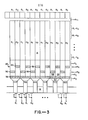
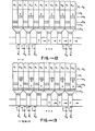
- FIG. 1 is a schematic of an SPS CCD array as disclosed in U. S. Patent No. 4,165,541.
- the CCD memory array 10 is arranged as a serial-parallel-serial memory and includes interlacing of data to and from the parallel registers and ripple clocking of the parallel shift registers to increase the bit storage capacity.
- a parallel shift register of the block shown includes nine groups of eight electrodes, to which ripple clock signals R 1 , R 2 ...R 8 , respectively, are applied, each group being capable of storing seven bits of information.
- An input serial register 12 includes 32 electrodes associated with each of the 0 ⁇ 1 and 0 ⁇ 2 clock signals for a total of 64 electrodes.
- serial input shift register 12 which is driven by clock signals 0 ⁇ 1 and 0 ⁇ 2 .
- the data are stepped across the serial shift register in a conventional two phase CCD manner.
- a signal 0 ⁇ TI is supplied to allow these bits of information, represented by charge packets stored beneath the serial register electrodes, to be transferred into the input electrode of every other parallel shift register 14.
- additional data are stepped into the serial shift register by application of signals 0 ⁇ 1 and p 2 .
- the application of the ripple clock signals results in the rippling movement of 64 bits of data in the parallel shift registers. That is, a blank potential well is moved backward in each group of eight electrodes of the parallel shift registers, thereby transferring the data forward one electrode for each eight electrodes that the blank moves backward.
- Signal 0T2 is applied to cause a transfer of the data from the output electrode of every other one of the 64 parallel shift registers to be transferred into corresponding alternating electrodes of the output serial shift register. These data are then stepped out of the output serial register by the application of signals 0 ⁇ 1 and 0 ⁇ 2 . As soon as the output serial register is vacant, another transfer from the parallel shift register is initiated.
- an additional gate 18 is provided.
- Signal V cc is applied to electrode 18 to provide an intermediate voltage level between the high level of 0 ⁇ 1 (or 0 ⁇ 2 ) and the low level of ⁇ 2 (or 0 ⁇ 1 ) to selectively block charge transfer to the low level clock 0 ⁇ 2 ( or 0 ⁇ 1 ) .
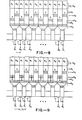
- FIGs 2A-2D illustrate charge transfer from the parallel registers 14 to the output serial register 16 of the array of Figure 1.
- the stored charge designated by x's
- the V cc electrodes 18 of the parallel registers are aligned awaiting transfer.
- the charges in the 0 ⁇ 1 registers are transferred to the output serial register 16 through the transfer gates 22 when 0 ⁇ 1 is high and 0 ⁇ 2 is low.
- the V cc voltage on electrodes 18 prevents the transfer of charge to the low 0 ⁇ 2 electrodes of output register 16.
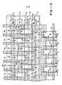
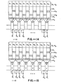
- FIG 3 is a schematic of one embodiment of an SPS CCD array in which the present invention can be employed.
- the array is similar to the array of Figure 1 and the same reference numerals are used for like elements.
- the endmost electrodes 20 of the parallel registers 14 are linearly offset with transfer gates 30 for transferring charge from the 0 ⁇ 1 columns to the output register being closer to the output register than the transfer gates 32 which transfer charge from the 0 ⁇ 2 columns of the parallel registers to the output register 16.
- the transfer gates 30 respond to a signal R B
- the transfer gates 32 respond to a signal R whereby charge from the 0 ⁇ 1 and 0 ⁇ 2 columns are selectively transferred through storage gates 34 and transfer gates 36 to the storage gates 37.
- the storage gates 34 are controlled by a signal R C and the transfer and storage gates 36 and 37 are controlled by a signal R D . Transfer to the storage gates of the output serial register 16 is controlled by the serial gate 0 ⁇ 1 .
- the interlacing of data from the parallel registers to the serial output register occurs at the endmost electrodes of the parallel registers and not at the output serial register.
- the requirement for an intermediate voltage V cc is obviated due to the staggered alignment of the endmost electrodes 20 of the parallel registers. Since charge is transferred to the serial register 16 from storage electrodes 37 in response to the serial register 0 ⁇ 1 clock, critical timing is not required.
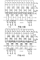
- Figures 4A-4D illustrate the transfer of charge from the parallel registers to the output serial register in the array of Figure 3.
- the charge in the 0 ⁇ 1 parallel registers is offset from the charge in the 0 ⁇ 2 registers due to charge in the 0 ⁇ 1 columns residing under storage gates 34 and charge in the ⁇ 2 columns being under electrodes 20.
- charge in the 1 columns is transferred from the storage gates 3 4 to the 0 ⁇ 1 electrodes of the output register 16. After this charge is moved from the output register, the charge in the 0 ⁇ 2 columns is transferred through the storage electrodes 37 to the serial register 16.
- This charge could be transferred to the 0 ⁇ 2 electrodes of register 16, by separate storage gates, but by sharing the storage gates 37 the charge can be transferred to the 0 ⁇ 1 electrodes, as will be described with reference to Figure 5.
- the charge can be removed from the output register by the two phase clocking.
- the intermediate voltage V cc is eliminated and the interlacing of the charge occurs in the slow transfer region of the parallel registers rather than at the fast transfer regions of the output serial register 16.
- critical timing in the charge transfer to the serial output register is eliminated by using the serial register clock for charge transfer.
- Figure 5 is a more detailed schematic of a portion of the array of Figure 3 in accordance with one embodiment of the present invention and further illustrating the endmost electrodes 20 of the parallel registers, the transfer gate electrodes 30 for the 0 ⁇ 1 channels, the transfer electrode 32 for the ⁇ 2 channels, the storage electrode 34, the transfer electrode 36 and the storage electrode 37.
- the structures are similar to the semiconductor structures in U. S. Patent No. 4,165,541, with the parallel channels defined by channel stop implant or by field oxide 40 and the doped barriers between electrodes in the parallel registers and the output serial register indicated by cross hatching 42.
- the transfer gates 30 and 32 are polycrystalline silicon, or polysilicon, electrodes overlying the barriers in the 0 ⁇ 1 channels and the 0 ⁇ 2 channels, respectively.
- Storage electrodes 34 are polysilicon overlying the 0 ⁇ 1 channels between the barriers 43 and the barriers 45 and overlying the 0 ⁇ 2 channels between the barriers 44 and the barriers 45.
- the charge from the storage gates 34 in the 0 ⁇ 1 and 0 ⁇ 2 columns can be respectively transferred through separate transfer gates to the serial output register 16.
- one storage gate 37 is used for two adjacent 0 ⁇ 1 and 0 ⁇ 2 columns whereby charge from the two columns are alternately transferred through the storage gate 37 to the 0 ⁇ 1 gates of the serial output register.
- the transfer gates 36 have a polysilicon electrode comprising polysilicon 48 overlying the doped barrier 45 and the storage gates 37 comprises polysilicon overlying the charge storage region.
- the 0 ⁇ 1 electrodes of the serial output register overlap barriers 52 between the storage gates 37 and the serial register.
- the endmost electrodes 20 of the two parallel columns are controlled by voltage R 1 .
- the transfer gates 30 and 32 are controlled by voltages R A and R Br respectively.
- Storage gate 34 is controlled by a voltage R C
- the transfer gate 36 and storage gate 37 are controlled by a voltage R D .
- Charge is transferred into a gate of the output serial register 16.
- the 0 ⁇ 1 and 9 2 signals for transferring charge in the serial registers are given along with the ripple voltages R 1 -R 8 for transferring charge in the parallel registers.
- the control voltages R A , R B , R C , and R D are then shown in time sequence with respect to the 0 ⁇ 1 and 0 ⁇ 2 voltages and the Rl-R8'ripple voltages.
- the charges in the 0 ⁇ 2 channels of parallel registers are transferred to the storage gates 34 in response to R A and R C .
- the charges in the storage gates 34 are then transferred to the storage gate 37 in response to R D for loading in the serial output register 16.
- the charges in the storage gate 37 are transferred into the output register 16 in response to the 0 ⁇ 1 voltage.
Landscapes
- Solid State Image Pick-Up Elements (AREA)
- Transforming Light Signals Into Electric Signals (AREA)
Applications Claiming Priority (4)
| Application Number | Priority Date | Filing Date | Title |
|---|---|---|---|
| US24178081A | 1981-03-09 | 1981-03-09 | |
| US24177581A | 1981-03-09 | 1981-03-09 | |
| US241775 | 1981-03-09 | ||
| US241780 | 1981-03-09 |
Publications (2)
| Publication Number | Publication Date |
|---|---|
| EP0060198A2 true EP0060198A2 (de) | 1982-09-15 |
| EP0060198A3 EP0060198A3 (de) | 1985-05-15 |
Family
ID=26934566
Family Applications (1)
| Application Number | Title | Priority Date | Filing Date |
|---|---|---|---|
| EP82400396A Withdrawn EP0060198A3 (de) | 1981-03-09 | 1982-03-08 | Seriell-parallel-seriell ladungsgekoppelte Speicheranordnung und Verfahren zur Übertragung einer darin enthaltenen Ladung |
Country Status (1)
| Country | Link |
|---|---|
| EP (1) | EP0060198A3 (de) |
Cited By (2)
| Publication number | Priority date | Publication date | Assignee | Title |
|---|---|---|---|---|
| US4669100A (en) * | 1981-11-30 | 1987-05-26 | U.S. Philips Corporation | Charge-coupled device having a buffer electrode |
| EP0314215A3 (de) * | 1987-10-28 | 1990-08-22 | Koninklijke Philips Electronics N.V. | Ladungsverschiebeschaltung |
Family Cites Families (4)
| Publication number | Priority date | Publication date | Assignee | Title |
|---|---|---|---|---|
| US3967254A (en) * | 1974-11-18 | 1976-06-29 | Rca Corporation | Charge transfer memory |
| US4211936A (en) * | 1978-06-16 | 1980-07-08 | Rca Corporation | CCD Gate electrode structures and systems employing the same |
| DE2836080B1 (de) * | 1978-08-17 | 1979-10-11 | Siemens Ag | Ladungsverschiebespeicher in Seriell-Pariellorganisation mit streng periodischer Taktansteuerung |
| US4288864A (en) * | 1979-10-24 | 1981-09-08 | International Business Machines Corporation | Serial-parallel-serial CCD memory system with fan out and fan in circuits |
-
1982
- 1982-03-08 EP EP82400396A patent/EP0060198A3/de not_active Withdrawn
Cited By (2)
| Publication number | Priority date | Publication date | Assignee | Title |
|---|---|---|---|---|
| US4669100A (en) * | 1981-11-30 | 1987-05-26 | U.S. Philips Corporation | Charge-coupled device having a buffer electrode |
| EP0314215A3 (de) * | 1987-10-28 | 1990-08-22 | Koninklijke Philips Electronics N.V. | Ladungsverschiebeschaltung |
Also Published As
| Publication number | Publication date |
|---|---|
| EP0060198A3 (de) | 1985-05-15 |
Similar Documents
| Publication | Publication Date | Title |
|---|---|---|
| US4493060A (en) | Serial-parallel-serial charged coupled device memory and a method of transferring charge therein | |
| US3967254A (en) | Charge transfer memory | |
| IL46895A (en) | C c d memory with interlaced storage | |
| JPS6236399B2 (de) | ||
| US4236830A (en) | CCD Parallel-serial and serial-parallel charge transfer method and apparatus | |
| EP0315778B1 (de) | Festkörperbildaufnahmevorrichtung | |
| US4669100A (en) | Charge-coupled device having a buffer electrode | |
| US4139910A (en) | Charge coupled device memory with method of doubled storage capacity and independent of process parameters and temperature | |
| EP0241800B1 (de) | Festkörpersbildsensor | |
| EP0060198A2 (de) | Seriell-parallel-seriell ladungsgekoppelte Speicheranordnung und Verfahren zur Übertragung einer darin enthaltenen Ladung | |
| EP0042477B1 (de) | Mit niedriger Spannung arbeitender Seriell-Parallel-Seriell-Ladungsverschiebespeicher | |
| US4539597A (en) | Solid state image pickup device | |
| CA1187177A (en) | Serial-parallel-serial charge coupled device and method of transferring charge therein | |
| EP0161023A1 (de) | Ladungsgekoppelte Halbleiteranordnung mit dynamischer Steuerung | |
| EP0314215A2 (de) | Ladungsverschiebeschaltung | |
| US4196389A (en) | Test site for a charged coupled device (CCD) array | |
| EP0496357B1 (de) | Ladungsgekoppelter Baustein | |
| US4288864A (en) | Serial-parallel-serial CCD memory system with fan out and fan in circuits | |
| US4241422A (en) | Series-parallel-series charge transfer memory having complete bias charge operation | |
| US4206370A (en) | Serial-parallel-loop CCD register | |
| EP0159758A1 (de) | Ladungsverschiebeanordnung | |
| JPH06121235A (ja) | 電荷転送素子の駆動方法 | |
| JPH0666346B2 (ja) | 電荷結合素子およびその駆動方法 | |
| JP2749700B2 (ja) | リニアイメージセンサ | |
| JPH11275464A (ja) | 電荷転送装置の駆動方法 |
Legal Events
| Date | Code | Title | Description |
|---|---|---|---|
| PUAI | Public reference made under article 153(3) epc to a published international application that has entered the european phase |
Free format text: ORIGINAL CODE: 0009012 |
|
| AK | Designated contracting states |
Designated state(s): DE FR GB IT NL |
|
| PUAL | Search report despatched |
Free format text: ORIGINAL CODE: 0009013 |
|
| AK | Designated contracting states |
Designated state(s): DE FR GB IT NL |
|
| STAA | Information on the status of an ep patent application or granted ep patent |
Free format text: STATUS: THE APPLICATION IS DEEMED TO BE WITHDRAWN |
|
| 18D | Application deemed to be withdrawn |
Effective date: 19860116 |
|
| RIN1 | Information on inventor provided before grant (corrected) |
Inventor name: VENKATESWARAN, KALYANASUNDARAM Inventor name: VARSHNEY, RAMESH C. |