EP0056737A2 - Procédé de fabrication d'un dispositif semi-conducteur employant l'épitaxie par faisceau moléculaire - Google Patents
Procédé de fabrication d'un dispositif semi-conducteur employant l'épitaxie par faisceau moléculaire Download PDFInfo
- Publication number
- EP0056737A2 EP0056737A2 EP82300288A EP82300288A EP0056737A2 EP 0056737 A2 EP0056737 A2 EP 0056737A2 EP 82300288 A EP82300288 A EP 82300288A EP 82300288 A EP82300288 A EP 82300288A EP 0056737 A2 EP0056737 A2 EP 0056737A2
- Authority
- EP
- European Patent Office
- Prior art keywords
- substrate
- evaporation
- layer
- film
- semiconductor device
- Prior art date
- Legal status (The legal status is an assumption and is not a legal conclusion. Google has not performed a legal analysis and makes no representation as to the accuracy of the status listed.)
- Withdrawn
Links
- 239000004065 semiconductor Substances 0.000 title claims abstract description 43
- 238000004519 manufacturing process Methods 0.000 title claims description 12
- 238000001451 molecular beam epitaxy Methods 0.000 title abstract description 12
- 239000000758 substrate Substances 0.000 claims abstract description 42
- 238000001704 evaporation Methods 0.000 claims abstract description 35
- 230000008020 evaporation Effects 0.000 claims abstract description 33
- 238000000034 method Methods 0.000 claims abstract description 26
- 229910052751 metal Inorganic materials 0.000 claims abstract description 25
- 239000002184 metal Substances 0.000 claims abstract description 24
- 239000012212 insulator Substances 0.000 claims abstract description 10
- 230000015572 biosynthetic process Effects 0.000 claims abstract description 5
- 239000012535 impurity Substances 0.000 claims description 13
- 239000000463 material Substances 0.000 claims description 11
- 230000002411 adverse Effects 0.000 abstract description 2
- 239000000969 carrier Substances 0.000 abstract description 2
- 239000010408 film Substances 0.000 description 81
- 239000011521 glass Substances 0.000 description 19
- 239000013078 crystal Substances 0.000 description 11
- VYPSYNLAJGMNEJ-UHFFFAOYSA-N Silicium dioxide Chemical compound O=[Si]=O VYPSYNLAJGMNEJ-UHFFFAOYSA-N 0.000 description 9
- 238000009834 vaporization Methods 0.000 description 8
- 229910052681 coesite Inorganic materials 0.000 description 7
- 150000001875 compounds Chemical class 0.000 description 7
- 229910052906 cristobalite Inorganic materials 0.000 description 7
- 230000000694 effects Effects 0.000 description 7
- 238000010894 electron beam technology Methods 0.000 description 7
- 239000007789 gas Substances 0.000 description 7
- 238000010438 heat treatment Methods 0.000 description 7
- 229910052682 stishovite Inorganic materials 0.000 description 7
- 229910052905 tridymite Inorganic materials 0.000 description 7
- 238000005468 ion implantation Methods 0.000 description 6
- 238000002844 melting Methods 0.000 description 5
- 229910021420 polycrystalline silicon Inorganic materials 0.000 description 5
- 239000000470 constituent Substances 0.000 description 4
- 238000009792 diffusion process Methods 0.000 description 4
- 230000008018 melting Effects 0.000 description 4
- 230000037230 mobility Effects 0.000 description 4
- 238000007738 vacuum evaporation Methods 0.000 description 4
- 229910001218 Gallium arsenide Inorganic materials 0.000 description 3
- XUIMIQQOPSSXEZ-UHFFFAOYSA-N Silicon Chemical compound [Si] XUIMIQQOPSSXEZ-UHFFFAOYSA-N 0.000 description 3
- QVGXLLKOCUKJST-UHFFFAOYSA-N atomic oxygen Chemical compound [O] QVGXLLKOCUKJST-UHFFFAOYSA-N 0.000 description 3
- 238000002513 implantation Methods 0.000 description 3
- 239000000203 mixture Substances 0.000 description 3
- 239000001301 oxygen Substances 0.000 description 3
- 229910052760 oxygen Inorganic materials 0.000 description 3
- 229910052710 silicon Inorganic materials 0.000 description 3
- 239000010703 silicon Substances 0.000 description 3
- 230000008016 vaporization Effects 0.000 description 3
- 230000015556 catabolic process Effects 0.000 description 2
- 238000005229 chemical vapour deposition Methods 0.000 description 2
- 238000002425 crystallisation Methods 0.000 description 2
- 230000006698 induction Effects 0.000 description 2
- 150000002739 metals Chemical class 0.000 description 2
- 229910052763 palladium Inorganic materials 0.000 description 2
- 229910052697 platinum Inorganic materials 0.000 description 2
- 238000002128 reflection high energy electron diffraction Methods 0.000 description 2
- 239000000377 silicon dioxide Substances 0.000 description 2
- 229910052719 titanium Inorganic materials 0.000 description 2
- 229910052721 tungsten Inorganic materials 0.000 description 2
- ZOXJGFHDIHLPTG-UHFFFAOYSA-N Boron Chemical compound [B] ZOXJGFHDIHLPTG-UHFFFAOYSA-N 0.000 description 1
- 229910052581 Si3N4 Inorganic materials 0.000 description 1
- -1 SiO2 Chemical class 0.000 description 1
- 230000001133 acceleration Effects 0.000 description 1
- 230000001464 adherent effect Effects 0.000 description 1
- 239000000956 alloy Substances 0.000 description 1
- 229910052782 aluminium Inorganic materials 0.000 description 1
- PNEYBMLMFCGWSK-UHFFFAOYSA-N aluminium oxide Inorganic materials [O-2].[O-2].[O-2].[Al+3].[Al+3] PNEYBMLMFCGWSK-UHFFFAOYSA-N 0.000 description 1
- 229910052796 boron Inorganic materials 0.000 description 1
- 150000001768 cations Chemical class 0.000 description 1
- 239000000919 ceramic Substances 0.000 description 1
- 238000006243 chemical reaction Methods 0.000 description 1
- 229910052804 chromium Inorganic materials 0.000 description 1
- 238000011109 contamination Methods 0.000 description 1
- 229910052593 corundum Inorganic materials 0.000 description 1
- 230000007547 defect Effects 0.000 description 1
- 238000006731 degradation reaction Methods 0.000 description 1
- 238000000151 deposition Methods 0.000 description 1
- 238000010586 diagram Methods 0.000 description 1
- 238000005516 engineering process Methods 0.000 description 1
- 230000005669 field effect Effects 0.000 description 1
- 229910052733 gallium Inorganic materials 0.000 description 1
- 229910052737 gold Inorganic materials 0.000 description 1
- 230000003993 interaction Effects 0.000 description 1
- 150000002500 ions Chemical class 0.000 description 1
- 230000001678 irradiating effect Effects 0.000 description 1
- 239000007788 liquid Substances 0.000 description 1
- 238000001459 lithography Methods 0.000 description 1
- 150000002736 metal compounds Chemical class 0.000 description 1
- 229910001092 metal group alloy Inorganic materials 0.000 description 1
- 229910052750 molybdenum Inorganic materials 0.000 description 1
- 229910052759 nickel Inorganic materials 0.000 description 1
- 238000002161 passivation Methods 0.000 description 1
- 238000004886 process control Methods 0.000 description 1
- 239000000126 substance Substances 0.000 description 1
- 229910052715 tantalum Inorganic materials 0.000 description 1
- 239000010409 thin film Substances 0.000 description 1
- 229910001845 yogo sapphire Inorganic materials 0.000 description 1
Images

Classifications
-
- H—ELECTRICITY
- H01—ELECTRIC ELEMENTS
- H01L—SEMICONDUCTOR DEVICES NOT COVERED BY CLASS H10
- H01L29/00—Semiconductor devices specially adapted for rectifying, amplifying, oscillating or switching and having potential barriers; Capacitors or resistors having potential barriers, e.g. a PN-junction depletion layer or carrier concentration layer; Details of semiconductor bodies or of electrodes thereof ; Multistep manufacturing processes therefor
- H01L29/66—Types of semiconductor device ; Multistep manufacturing processes therefor
- H01L29/66007—Multistep manufacturing processes
- H01L29/66075—Multistep manufacturing processes of devices having semiconductor bodies comprising group 14 or group 13/15 materials
- H01L29/66227—Multistep manufacturing processes of devices having semiconductor bodies comprising group 14 or group 13/15 materials the devices being controllable only by the electric current supplied or the electric potential applied, to an electrode which does not carry the current to be rectified, amplified or switched, e.g. three-terminal devices
- H01L29/66409—Unipolar field-effect transistors
- H01L29/66477—Unipolar field-effect transistors with an insulated gate, i.e. MISFET
- H01L29/66742—Thin film unipolar transistors
- H01L29/6675—Amorphous silicon or polysilicon transistors
- H01L29/66757—Lateral single gate single channel transistors with non-inverted structure, i.e. the channel layer is formed before the gate
-
- C—CHEMISTRY; METALLURGY
- C23—COATING METALLIC MATERIAL; COATING MATERIAL WITH METALLIC MATERIAL; CHEMICAL SURFACE TREATMENT; DIFFUSION TREATMENT OF METALLIC MATERIAL; COATING BY VACUUM EVAPORATION, BY SPUTTERING, BY ION IMPLANTATION OR BY CHEMICAL VAPOUR DEPOSITION, IN GENERAL; INHIBITING CORROSION OF METALLIC MATERIAL OR INCRUSTATION IN GENERAL
- C23C—COATING METALLIC MATERIAL; COATING MATERIAL WITH METALLIC MATERIAL; SURFACE TREATMENT OF METALLIC MATERIAL BY DIFFUSION INTO THE SURFACE, BY CHEMICAL CONVERSION OR SUBSTITUTION; COATING BY VACUUM EVAPORATION, BY SPUTTERING, BY ION IMPLANTATION OR BY CHEMICAL VAPOUR DEPOSITION, IN GENERAL
- C23C14/00—Coating by vacuum evaporation, by sputtering or by ion implantation of the coating forming material
- C23C14/22—Coating by vacuum evaporation, by sputtering or by ion implantation of the coating forming material characterised by the process of coating
- C23C14/56—Apparatus specially adapted for continuous coating; Arrangements for maintaining the vacuum, e.g. vacuum locks
-
- H—ELECTRICITY
- H01—ELECTRIC ELEMENTS
- H01L—SEMICONDUCTOR DEVICES NOT COVERED BY CLASS H10
- H01L21/00—Processes or apparatus adapted for the manufacture or treatment of semiconductor or solid state devices or of parts thereof
- H01L21/02—Manufacture or treatment of semiconductor devices or of parts thereof
- H01L21/02104—Forming layers
- H01L21/02107—Forming insulating materials on a substrate
- H01L21/02109—Forming insulating materials on a substrate characterised by the type of layer, e.g. type of material, porous/non-porous, pre-cursors, mixtures or laminates
- H01L21/02112—Forming insulating materials on a substrate characterised by the type of layer, e.g. type of material, porous/non-porous, pre-cursors, mixtures or laminates characterised by the material of the layer
- H01L21/02123—Forming insulating materials on a substrate characterised by the type of layer, e.g. type of material, porous/non-porous, pre-cursors, mixtures or laminates characterised by the material of the layer the material containing silicon
- H01L21/02164—Forming insulating materials on a substrate characterised by the type of layer, e.g. type of material, porous/non-porous, pre-cursors, mixtures or laminates characterised by the material of the layer the material containing silicon the material being a silicon oxide, e.g. SiO2
-
- H—ELECTRICITY
- H01—ELECTRIC ELEMENTS
- H01L—SEMICONDUCTOR DEVICES NOT COVERED BY CLASS H10
- H01L21/00—Processes or apparatus adapted for the manufacture or treatment of semiconductor or solid state devices or of parts thereof
- H01L21/02—Manufacture or treatment of semiconductor devices or of parts thereof
- H01L21/02104—Forming layers
- H01L21/02107—Forming insulating materials on a substrate
- H01L21/02109—Forming insulating materials on a substrate characterised by the type of layer, e.g. type of material, porous/non-porous, pre-cursors, mixtures or laminates
- H01L21/02112—Forming insulating materials on a substrate characterised by the type of layer, e.g. type of material, porous/non-porous, pre-cursors, mixtures or laminates characterised by the material of the layer
- H01L21/02172—Forming insulating materials on a substrate characterised by the type of layer, e.g. type of material, porous/non-porous, pre-cursors, mixtures or laminates characterised by the material of the layer the material containing at least one metal element, e.g. metal oxides, metal nitrides, metal oxynitrides or metal carbides
- H01L21/02175—Forming insulating materials on a substrate characterised by the type of layer, e.g. type of material, porous/non-porous, pre-cursors, mixtures or laminates characterised by the material of the layer the material containing at least one metal element, e.g. metal oxides, metal nitrides, metal oxynitrides or metal carbides characterised by the metal
- H01L21/02178—Forming insulating materials on a substrate characterised by the type of layer, e.g. type of material, porous/non-porous, pre-cursors, mixtures or laminates characterised by the material of the layer the material containing at least one metal element, e.g. metal oxides, metal nitrides, metal oxynitrides or metal carbides characterised by the metal the material containing aluminium, e.g. Al2O3
-
- H—ELECTRICITY
- H01—ELECTRIC ELEMENTS
- H01L—SEMICONDUCTOR DEVICES NOT COVERED BY CLASS H10
- H01L21/00—Processes or apparatus adapted for the manufacture or treatment of semiconductor or solid state devices or of parts thereof
- H01L21/02—Manufacture or treatment of semiconductor devices or of parts thereof
- H01L21/02104—Forming layers
- H01L21/02107—Forming insulating materials on a substrate
- H01L21/02225—Forming insulating materials on a substrate characterised by the process for the formation of the insulating layer
- H01L21/0226—Forming insulating materials on a substrate characterised by the process for the formation of the insulating layer formation by a deposition process
- H01L21/02263—Forming insulating materials on a substrate characterised by the process for the formation of the insulating layer formation by a deposition process deposition from the gas or vapour phase
- H01L21/02269—Forming insulating materials on a substrate characterised by the process for the formation of the insulating layer formation by a deposition process deposition from the gas or vapour phase deposition by thermal evaporation
-
- H—ELECTRICITY
- H01—ELECTRIC ELEMENTS
- H01L—SEMICONDUCTOR DEVICES NOT COVERED BY CLASS H10
- H01L21/00—Processes or apparatus adapted for the manufacture or treatment of semiconductor or solid state devices or of parts thereof
- H01L21/02—Manufacture or treatment of semiconductor devices or of parts thereof
- H01L21/02104—Forming layers
- H01L21/02365—Forming inorganic semiconducting materials on a substrate
- H01L21/02367—Substrates
- H01L21/0237—Materials
- H01L21/02373—Group 14 semiconducting materials
- H01L21/02381—Silicon, silicon germanium, germanium
-
- H—ELECTRICITY
- H01—ELECTRIC ELEMENTS
- H01L—SEMICONDUCTOR DEVICES NOT COVERED BY CLASS H10
- H01L21/00—Processes or apparatus adapted for the manufacture or treatment of semiconductor or solid state devices or of parts thereof
- H01L21/02—Manufacture or treatment of semiconductor devices or of parts thereof
- H01L21/02104—Forming layers
- H01L21/02365—Forming inorganic semiconducting materials on a substrate
- H01L21/02367—Substrates
- H01L21/0237—Materials
- H01L21/02422—Non-crystalline insulating materials, e.g. glass, polymers
-
- H—ELECTRICITY
- H01—ELECTRIC ELEMENTS
- H01L—SEMICONDUCTOR DEVICES NOT COVERED BY CLASS H10
- H01L21/00—Processes or apparatus adapted for the manufacture or treatment of semiconductor or solid state devices or of parts thereof
- H01L21/02—Manufacture or treatment of semiconductor devices or of parts thereof
- H01L21/02104—Forming layers
- H01L21/02365—Forming inorganic semiconducting materials on a substrate
- H01L21/02436—Intermediate layers between substrates and deposited layers
- H01L21/02439—Materials
- H01L21/02441—Group 14 semiconducting materials
- H01L21/0245—Silicon, silicon germanium, germanium
-
- H—ELECTRICITY
- H01—ELECTRIC ELEMENTS
- H01L—SEMICONDUCTOR DEVICES NOT COVERED BY CLASS H10
- H01L21/00—Processes or apparatus adapted for the manufacture or treatment of semiconductor or solid state devices or of parts thereof
- H01L21/02—Manufacture or treatment of semiconductor devices or of parts thereof
- H01L21/02104—Forming layers
- H01L21/02365—Forming inorganic semiconducting materials on a substrate
- H01L21/02436—Intermediate layers between substrates and deposited layers
- H01L21/02439—Materials
- H01L21/02488—Insulating materials
-
- H—ELECTRICITY
- H01—ELECTRIC ELEMENTS
- H01L—SEMICONDUCTOR DEVICES NOT COVERED BY CLASS H10
- H01L21/00—Processes or apparatus adapted for the manufacture or treatment of semiconductor or solid state devices or of parts thereof
- H01L21/02—Manufacture or treatment of semiconductor devices or of parts thereof
- H01L21/02104—Forming layers
- H01L21/02365—Forming inorganic semiconducting materials on a substrate
- H01L21/02436—Intermediate layers between substrates and deposited layers
- H01L21/02439—Materials
- H01L21/02491—Conductive materials
-
- H—ELECTRICITY
- H01—ELECTRIC ELEMENTS
- H01L—SEMICONDUCTOR DEVICES NOT COVERED BY CLASS H10
- H01L21/00—Processes or apparatus adapted for the manufacture or treatment of semiconductor or solid state devices or of parts thereof
- H01L21/02—Manufacture or treatment of semiconductor devices or of parts thereof
- H01L21/02104—Forming layers
- H01L21/02365—Forming inorganic semiconducting materials on a substrate
- H01L21/02518—Deposited layers
- H01L21/02521—Materials
- H01L21/02524—Group 14 semiconducting materials
- H01L21/02532—Silicon, silicon germanium, germanium
-
- H—ELECTRICITY
- H01—ELECTRIC ELEMENTS
- H01L—SEMICONDUCTOR DEVICES NOT COVERED BY CLASS H10
- H01L21/00—Processes or apparatus adapted for the manufacture or treatment of semiconductor or solid state devices or of parts thereof
- H01L21/02—Manufacture or treatment of semiconductor devices or of parts thereof
- H01L21/02104—Forming layers
- H01L21/02365—Forming inorganic semiconducting materials on a substrate
- H01L21/02612—Formation types
- H01L21/02617—Deposition types
- H01L21/02631—Physical deposition at reduced pressure, e.g. MBE, sputtering, evaporation
-
- H—ELECTRICITY
- H01—ELECTRIC ELEMENTS
- H01L—SEMICONDUCTOR DEVICES NOT COVERED BY CLASS H10
- H01L21/00—Processes or apparatus adapted for the manufacture or treatment of semiconductor or solid state devices or of parts thereof
- H01L21/02—Manufacture or treatment of semiconductor devices or of parts thereof
- H01L21/04—Manufacture or treatment of semiconductor devices or of parts thereof the devices having potential barriers, e.g. a PN junction, depletion layer or carrier concentration layer
- H01L21/18—Manufacture or treatment of semiconductor devices or of parts thereof the devices having potential barriers, e.g. a PN junction, depletion layer or carrier concentration layer the devices having semiconductor bodies comprising elements of Group IV of the Periodic Table or AIIIBV compounds with or without impurities, e.g. doping materials
- H01L21/30—Treatment of semiconductor bodies using processes or apparatus not provided for in groups H01L21/20 - H01L21/26
- H01L21/31—Treatment of semiconductor bodies using processes or apparatus not provided for in groups H01L21/20 - H01L21/26 to form insulating layers thereon, e.g. for masking or by using photolithographic techniques; After treatment of these layers; Selection of materials for these layers
- H01L21/3205—Deposition of non-insulating-, e.g. conductive- or resistive-, layers on insulating layers; After-treatment of these layers
- H01L21/32051—Deposition of metallic or metal-silicide layers
-
- H—ELECTRICITY
- H01—ELECTRIC ELEMENTS
- H01L—SEMICONDUCTOR DEVICES NOT COVERED BY CLASS H10
- H01L2924/00—Indexing scheme for arrangements or methods for connecting or disconnecting semiconductor or solid-state bodies as covered by H01L24/00
- H01L2924/0001—Technical content checked by a classifier
- H01L2924/0002—Not covered by any one of groups H01L24/00, H01L24/00 and H01L2224/00
Definitions
- This invention relates to a method of manufacturing a semiconductor device employing evaporation under ultra-high vacuum (usually called "molecular-beam epitaxy process" - abbreviated to MBE process).
- the present invention provides a method of manufacturing a semiconductor device, including the step of evacuating a vacuum vessel to an ultra-high vacuum, the vessel containing a first evaporation source and a substrate having a surface onto which a layer is to be evaporated; and the step of forming a first evaporation layer on said surface using the first evaporation source; characterised in that the vacuum vessel contains at least a second evaporation source, and the method includes the step of subsequently forming a second evaporation layer on the first evaporation layer, using the second evaporation source, without removing the substrate from the vacuum vessel between the formation of the first and second evaporation layers.
- One of the evaporation sources can be a semiconductor material and another an insulator material.
- the pressure of the vacuum is at most 10 Torr.
- further substances can be evaporated into multilayer films as may be needed.
- the size of the semiconductor device is limited first by the size of the substrate.
- a silicon substrate is limited to a size of approximately 75 mm x 75 mm.
- the present invention forms multilayer films consecutively within the same vessel, the films do not touch the outside air containing many contamination sources, and hence, not only the formed films themselves but also the interfaces of the respective films are kept clean. For this reason, the multilayer films obtained are free from the occurrence of a surface state, are very stable without fluctuations and exhibit good characteristics. More specifically, it is a matter of course that when adsorbed in a film to be'formed, residual gases such as the air degrade the characteristics of the film. Even when a film has been formed clean, once the film is exposed to the outside air or the like, various kinds of molecules contained in the atmosphere adhere to the surface thereof. When a further film is formed with the molecules left adherent, these molecules degrade the respective films directly or indirectly.
- the multilayer films which have been formed bearing the impure molecules etc. in this manner are used in a device, they have evil effects on the electr.ical characteristics of the device such as the threshold voltage and the breakdown voltage or on the design and control of the device. With our preferred multilayer films, factors allowing such degradation are fully eliminated, and good multilayer films can be formed without any such problems.
- Such multilayer films are very effective when utilised for the formation of a semiconductor device, especially a semiconductor element sensitive to the surface state, such as MOSFET (MOS type Field Effect Transistor).
- MOSFET MOS type Field Effect Transistor
- the mean free path is several km to several hundred km, and the scattering molecules are not hindered by the foreign residual gas molecules or impurity atoms, so that they are grown on the glass as a crystal.
- the substrate is below room temperature, kinetic energy required for the crystallisation is insufficient, and the growth of a crystal film of good quality is not attained.
- the softening point of the substrate glass is exceeded, the substrate is melted or transformed, so that the crystal film is not grown.
- the glass substrate is not a crystalline body, but it is usually a non-crystalline body (amorphous or vitreous). In the ultra-high vacuum atmosphere,. however, the film to be formed on the glass substrate has the property of becoming a crystal layer as stated before.
- the degree of vacuum during the evaporation is suitably below 1 x 10 -8 Torr in terms of pressure, and the partial pressure of oxygen is below 1 x 10⁻⁹ Torr.
- an insulating film is formed within the aforecited ultra-high vacuum. Since the insulating film is ordinarily a compound such as SiO 2 , Si 3 N 4 and A1203, a method of evaporation as described below may be adopted.
- the Si film has light or an electron beam directed thereon or is irradiated with nascent oxygen.
- the molecular beam-generating vessel may well be a vessel in the shape of a crucible round which a resistive heater is wound.
- a vessel which is capable of electron-beam heating, induction heating or the like is used.
- a metal film is to be formed on the semiconductor film, it is quite similarly formed within the aforecited ultra-high vacuum.
- a metal element of high melting point such as Mo, Ta, Pd, Pt, W and Ti is evaporated by putting it into a metal molecular beam likewise to the case of the semiconductor.
- the present invention preferably consists in evaporating films by irradiating a substrate at a low temper.ature with the molecular beam of the respective evaporation sources within ultra-high vacuum. Therefore, even when the evaporation sources include materials of quite different natures such as a semiconductor, insulator and metal, the films can be continuously and successively grown without possessing any foreign molecule or residual gas exerting an adverse effect, in the interfaces and the materials.
- Various means can be used to generate the molecular beam, including the foregoing methods using an electron beam and r. f. heating, and methods using a laser beam or a plasma exhibit quite similar effects.
- a vacuum vessel 11 is held under an ultra-high vacuum condition with a pressure of at most 10 Torr.
- the fore end part (surface part) of a Si source l24 is held in a melted state by an electron beam 123 emitted from an E (Electron) gun-system 122, and a molecular beam of Si is generated.
- the electron beam 123 is deflected by an external magnetic field so as to collide against the Si source 124.
- an Si film can be epitaxially grown on a glass substrate 13 at a rate of 1 - 100 ⁇ /second.
- the Si grows up on the substrate 13 to a film thickness of 500 ⁇ to several pm under a polycrystalline state.
- an insulating film is formed on the Si film.
- a vaporization source 12 is used to form a molecular beam of Sio 2 by way of example so as to deposit the Si0 2 on the polycrystalline film.
- the vaporised Si0 2 molecules .reach the glass substrate 13 through an aperture 141 which is provided in a shroud 14.
- Vaporisation sources 12',12" and 121 are used as are needed for the compositions of films to be formed.
- the clean state of the substrate 13 before the growth or the surface structure of the grown layer can be immediately known by the use of an RHEED (Reflection High Energy Electron Diffraction) device which consists of an electron gun 15 and a fluorescent screen 16 as well as a controller 17 thereof, these being mounted on predetermined positions of the vacuum vessel 11.
- RHEED Reflect High Energy Electron Diffraction
- a mass spectrometer 18 which is placed in opposition to the vaporisation source 12 or 124 (and if necessary, to the sources 12',12" and 121) measures the kinds and quantities of residual gases and the quantities of respective constituent elements given forth from the vaporisation sources 12,124 etc.
- This information is inputted to a computer 19 for process control.
- the growth rate, the thickness of the film, the composition ratio of a mixed crystal and the impurity concentration which have been calculated by the computer are immediately displayed on a cathode-ray tube 191 and plotted on a recorder 192. Simultaneously therewith, they are fed back to the temperature control of a molecular-beam generator vessel (vaporization source oven).
- the vaporization source 121 is connected to the computer controller 19.
- the crystal growth is entirely programmed, and films of a multilayer structure are formed.
- the vapor growth or liquid growth which is.presently used as the epitaxial growth process of semiconductor films, only the temperature is obtained as an information during the crystal growth.
- MBE is a film growing method which is really rich in controllability.
- the epitaxial growth of a compound semiconductor such as GaAs since the vapor pressures of the constituent elements are remarkably different, obtaining of the compound at the stoichiometric ratio is difficult merely by vaporising a GaAs bulk or the like material as it is.
- a compound at the predetermined stoichiometric ratio is obtained by the so-called three- temperature method in which the elements of the composition are vaporised from individual vaporisation sources and in which the component of the higher vapor pressure is supplied in excess. Also in this case, since the interior of the evaporation chamber is under ultra-high vacuum, a crystal at the stoichiometric ratio can be grown merely by causing the beams of the constituent elements of the different vapor pressures to reach the substrate.
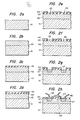
- Figures 2a - 2h are schematic flow diagrams of a semiconductor device which was formed by the use of the present invention.
- a transparent glass substrate 41 was prepared.
- an Si thin layer 42 having a thickness of 500 ⁇ to several ⁇ m is formed on the substrate 41, by heating a first evaporation source (an Si bar) with an electron beam by the ultra-high vacuum evaporation apparatus described before.
- a first evaporation source an Si bar
- the Si thin layer becomes polycrystalline.
- An Si molecular beam vaporised from the molecular beam source employing an electron gun is deposited within the ultra-high vacuum atmosphere which has a base vacuum degree of at most 10 -9 Torr.
- the substrate 41 is held at 500 o C (usually, at 400 - 650°C).
- a doping source for the impurity doping is packed in another crucible and is heated for the doping separately from the Si source.
- an Si0 2 film 43 is vacuum-evaporated on the Si thin layer 42 in the ultra-high vacuum atmosphere.
- the oxide film 43 suffices with a thickness of about 0.3 pm.
- a Mo film 44 is formed on the oxide film 43 by vacuum evaporation within the ultra-high vacuum atmosphere.
- a Mo piece is inserted in a crucible in advance. It is melted by a heating method utilizing induction heating, an electron beam or the like. Further, high-melting metals such as N i, W, Ti, Cr, Pd and Pt can be similarly used. Of course, metal elements or alloys of comparatively low melting points, such as Au and Al, may be similarly employed. In this case, the crucible may be at a comparatively low temperature, e.g. heated by electric resistance heating.
- the films of the semiconductor, insulator and metal which have properties different from one another are successively stacked on the glass substrate, whereupon the resultant structure is taken out of the ultra-high vacuum vessel so as to form a semiconductor device by the conventional semiconductor element-producing technology.
- windows 45 for diffusing a conductivity type impurity are formed in the Mo film 44, and windows 46 are subsequently formed in the oxide film 43 by utilizing the windows 45.
- the metal film 44 serves as an implantation mask, and hence, the oxide film 43 may well remain in the implantation windows.
- diffusion windows 46 extending down to the Si film 42 are, of course, used.
- diffusion regions 47. of a p-conductivity type impurity are formed in the Si thin layer 42 through the implantation windows.
- boron is turned into cations, which are implanted at an acceleration voltage of 200 keV and at a dose of about 3 x 10 15 /cm 2 .
- the resultant structure is annealed at 500°C for about 1 hour, to complete the conductive regions.
- the conductive regions may be similarly formed by conventional thermal diffusion.
- the conductive regions 47 formed function as the source and drain regions of the MOS transistor.
- metal electrodes 48 of Al are formed by conventional vacuum evaporation or the like as shown in Figure 2h. External,lead wires are connected to the metal electrodes. Then, the MOS transistor is completed.
- the device is depicted as a discrete component element provided with lead wires, it is needless to say that in the case of an IC etc., the electrodes are connected by stripe-shaped metal films.
- a gate oxide film 431 formed by this method is very clean, and the transistor manufactured by the above steps exhibits good characteristics. This is because, during the ion implantation, the metal film 44 prevents the ions from being introduced into the oxide film 43. Such effect does not depend upon the sort of the metal. Similar effects are achieved even with the various metals mentioned previously. Owing to the effect, no defect which gives rise to a surface state which lowers the mobility of the transistor is observed in the gate oxide film 431. Thus, the mobility of the polycrystalline silicon film-transistor has been improved by a factor of two or more. Naturally, the prior-art step of removing contaminated oxide films together after the ion implantation is dispensed with, so that the process for forming a device is remarkably simplified.
- the metal film 44 can be used as an electrode as it is, and this point is greatly advantageous in the process.
- the present invention is very effective for preventing a predetermined region such as a channel region from being contaminated due to the impurity doping.
- the example described above in detail has a great industrial merit in that in forming multilayer films by continuously evaporating a semiconductor film, insulating film, metal film etc. on a predetermined substrate within an ultra-high vacuum vessel, the interfaces of the films can be made clean.
- Si has been exemplified as a semiconductor material.
- other semiconductor materials for example, Ge or a compound semiconductor such as GaAs and GaAlAs are used, quite similar effects are achieved. That is, the interfaces of the layers of the various materials are very good.
- an impurity is ion-implanted into a material layer underlying a metal layer through an opening provided in the metal layer, there is the advantage that the impurity can be introduced locally into the part corresponding to the opening, without being mixed into unnecessary parts.
Landscapes
- Engineering & Computer Science (AREA)
- Microelectronics & Electronic Packaging (AREA)
- Power Engineering (AREA)
- Physics & Mathematics (AREA)
- Condensed Matter Physics & Semiconductors (AREA)
- General Physics & Mathematics (AREA)
- Manufacturing & Machinery (AREA)
- Computer Hardware Design (AREA)
- Chemical & Material Sciences (AREA)
- Materials Engineering (AREA)
- Ceramic Engineering (AREA)
- Chemical Kinetics & Catalysis (AREA)
- Mechanical Engineering (AREA)
- Metallurgy (AREA)
- Organic Chemistry (AREA)
- Physical Deposition Of Substances That Are Components Of Semiconductor Devices (AREA)
- Electrodes Of Semiconductors (AREA)
Applications Claiming Priority (2)
| Application Number | Priority Date | Filing Date | Title |
|---|---|---|---|
| JP56006395A JPS57121219A (en) | 1981-01-21 | 1981-01-21 | Manufacture of semiconductor device |
| JP6395/81 | 1981-01-21 |
Publications (2)
| Publication Number | Publication Date |
|---|---|
| EP0056737A2 true EP0056737A2 (fr) | 1982-07-28 |
| EP0056737A3 EP0056737A3 (fr) | 1983-06-29 |
Family
ID=11637174
Family Applications (1)
| Application Number | Title | Priority Date | Filing Date |
|---|---|---|---|
| EP82300288A Withdrawn EP0056737A3 (fr) | 1981-01-21 | 1982-01-20 | Procédé de fabrication d'un dispositif semi-conducteur employant l'épitaxie par faisceau moléculaire |
Country Status (3)
| Country | Link |
|---|---|
| EP (1) | EP0056737A3 (fr) |
| JP (1) | JPS57121219A (fr) |
| CA (1) | CA1184020A (fr) |
Cited By (4)
| Publication number | Priority date | Publication date | Assignee | Title |
|---|---|---|---|---|
| EP0113983A1 (fr) * | 1982-12-16 | 1984-07-25 | Fujitsu Limited | Fabrication d'un dispositif semi-conducteur au moyen d'épitaxie par faisceau moléculaire |
| US4477311A (en) * | 1982-12-28 | 1984-10-16 | Fujitsu Limited | Process and apparatus for fabricating a semiconductor device |
| EP0127838A2 (fr) * | 1983-06-06 | 1984-12-12 | International Business Machines Corporation | Sources de silicium pour dépôt épitaxial par faisceau moléculaire |
| WO2016201526A1 (fr) * | 2015-06-19 | 2016-12-22 | Chee Yee Kwok | Film de silicium et procédé pour former un film de silicium |
Families Citing this family (1)
| Publication number | Priority date | Publication date | Assignee | Title |
|---|---|---|---|---|
| JPH02172226A (ja) * | 1988-12-23 | 1990-07-03 | Nec Corp | シリコン酸化膜の形成方法及び形成装置 |
Citations (1)
| Publication number | Priority date | Publication date | Assignee | Title |
|---|---|---|---|---|
| US3928092A (en) * | 1974-08-28 | 1975-12-23 | Bell Telephone Labor Inc | Simultaneous molecular beam deposition of monocrystalline and polycrystalline III(a)-V(a) compounds to produce semiconductor devices |
Family Cites Families (1)
| Publication number | Priority date | Publication date | Assignee | Title |
|---|---|---|---|---|
| JPS5391573A (en) * | 1977-01-21 | 1978-08-11 | Mitsubishi Electric Corp | Molecular-beam epitaxial growth equipment |
-
1981
- 1981-01-21 JP JP56006395A patent/JPS57121219A/ja active Pending
-
1982
- 1982-01-20 CA CA000394515A patent/CA1184020A/fr not_active Expired
- 1982-01-20 EP EP82300288A patent/EP0056737A3/fr not_active Withdrawn
Patent Citations (1)
| Publication number | Priority date | Publication date | Assignee | Title |
|---|---|---|---|---|
| US3928092A (en) * | 1974-08-28 | 1975-12-23 | Bell Telephone Labor Inc | Simultaneous molecular beam deposition of monocrystalline and polycrystalline III(a)-V(a) compounds to produce semiconductor devices |
Non-Patent Citations (2)
| Title |
|---|
| IBM TECHNICAL DISCLOSURE BULLETIN, vol. 15, no. 2 , July 1972, New York L.L. CHANG et al. "Fabrication for multilayer semiconductor devices" * |
| IEEE SPECTRUM; vol. 17, no. 4, April 1980, New York M.G. PANISH et al. "Molecular beam epitaxy", pages 18-23 * |
Cited By (6)
| Publication number | Priority date | Publication date | Assignee | Title |
|---|---|---|---|---|
| EP0113983A1 (fr) * | 1982-12-16 | 1984-07-25 | Fujitsu Limited | Fabrication d'un dispositif semi-conducteur au moyen d'épitaxie par faisceau moléculaire |
| EP0208851A1 (fr) * | 1982-12-16 | 1987-01-21 | Fujitsu Limited | Fabrication d'un dispositif semi-conducteur au moyen d'épitaxie par faisceau moléculaire |
| US4477311A (en) * | 1982-12-28 | 1984-10-16 | Fujitsu Limited | Process and apparatus for fabricating a semiconductor device |
| EP0127838A2 (fr) * | 1983-06-06 | 1984-12-12 | International Business Machines Corporation | Sources de silicium pour dépôt épitaxial par faisceau moléculaire |
| EP0127838A3 (en) * | 1983-06-06 | 1987-05-20 | International Business Machines Corporation | Silicon sources suitable for use in molecular beam epitaxy deposition |
| WO2016201526A1 (fr) * | 2015-06-19 | 2016-12-22 | Chee Yee Kwok | Film de silicium et procédé pour former un film de silicium |
Also Published As
| Publication number | Publication date |
|---|---|
| JPS57121219A (en) | 1982-07-28 |
| EP0056737A3 (fr) | 1983-06-29 |
| CA1184020A (fr) | 1985-03-19 |
Similar Documents
| Publication | Publication Date | Title |
|---|---|---|
| US4800100A (en) | Combined ion and molecular beam apparatus and method for depositing materials | |
| US4888202A (en) | Method of manufacturing thin compound oxide film and apparatus for manufacturing thin oxide film | |
| US6080643A (en) | Elimination of dehydrogenation step when forming a silicon thin film device by low-temperature laser-annealing | |
| US3992233A (en) | Surface treatment of III-V compound crystals | |
| KR100229698B1 (ko) | 플라즈마 이온 방사를 이용한 soi 기판의 형성 방법 및 장치 | |
| EP0055032B1 (fr) | Transistor à effet de champ | |
| EP0056737A2 (fr) | Procédé de fabrication d'un dispositif semi-conducteur employant l'épitaxie par faisceau moléculaire | |
| KR20190024675A (ko) | 금속 칼코겐 화합물 박막의 제조 방법 | |
| GB1602386A (en) | Method of manufacturing semiconductor devices | |
| US7492086B1 (en) | Low work function emitters and method for production of FED's | |
| US4233613A (en) | Compound semiconductor wafer | |
| US4698235A (en) | Siting a film onto a substrate including electron-beam evaporation | |
| EP0215436B1 (fr) | Méthode de croissance d'une couche mince pour semi-conducteur composite | |
| Feldman et al. | Mass spectra analyses of impurities and ion clusters in amorphous and crystalline silicon films | |
| CN108085742B (zh) | 形成过渡金属二硫属化物(tmdc)材料层的方法 | |
| JPH0476217B2 (fr) | ||
| EP0107325A2 (fr) | Procédé de production de films d'oxyde | |
| US20030151051A1 (en) | High performance active and passive structures based on silicon material grown epitaxially or bonded to silicon carbide substrate | |
| JP3392507B2 (ja) | 微小電界放出陰極素子 | |
| JP2001110725A (ja) | ヘテロ構造半導体多層薄膜の製造方法 | |
| JP2881929B2 (ja) | アルミナ膜の製造方法 | |
| JPS584920A (ja) | 半導体の製造方法 | |
| JPS583221A (ja) | イオンビ−ム堆積法 | |
| WO2000062335A1 (fr) | Fabrication de plaquettes multicouches | |
| Kang et al. | Design and Analysis of GAIVBE System and Application to the Growth of Semiconductor Thin Films-On the Growth of GaAs on Si |
Legal Events
| Date | Code | Title | Description |
|---|---|---|---|
| PUAI | Public reference made under article 153(3) epc to a published international application that has entered the european phase |
Free format text: ORIGINAL CODE: 0009012 |
|
| 17P | Request for examination filed |
Effective date: 19820304 |
|
| AK | Designated contracting states |
Designated state(s): DE FR GB NL |
|
| PUAL | Search report despatched |
Free format text: ORIGINAL CODE: 0009013 |
|
| AK | Designated contracting states |
Designated state(s): DE FR GB NL |
|
| STAA | Information on the status of an ep patent application or granted ep patent |
Free format text: STATUS: THE APPLICATION IS DEEMED TO BE WITHDRAWN |
|
| 18D | Application deemed to be withdrawn |
Effective date: 19850720 |
|
| RIN1 | Information on inventor provided before grant (corrected) |
Inventor name: KOBAYASHI, KEISUKE L I Inventor name: MURAYAMA, YOSHIMASA Inventor name: MATSUI, MAKOTO Inventor name: SHIRAKI, YASUHIRO |