EP0055670A2 - Duty cycle control circuit for a periodic pulse signal, and 2n frequency multiplier including this circuit - Google Patents
Duty cycle control circuit for a periodic pulse signal, and 2n frequency multiplier including this circuit Download PDFInfo
- Publication number
- EP0055670A2 EP0055670A2 EP81402071A EP81402071A EP0055670A2 EP 0055670 A2 EP0055670 A2 EP 0055670A2 EP 81402071 A EP81402071 A EP 81402071A EP 81402071 A EP81402071 A EP 81402071A EP 0055670 A2 EP0055670 A2 EP 0055670A2
- Authority
- EP
- European Patent Office
- Prior art keywords
- flop
- circuit
- flip
- duty cycle
- input
- Prior art date
- Legal status (The legal status is an assumption and is not a legal conclusion. Google has not performed a legal analysis and makes no representation as to the accuracy of the status listed.)
- Granted
Links
Images
Classifications
-
- H—ELECTRICITY
- H03—ELECTRONIC CIRCUITRY
- H03K—PULSE TECHNIQUE
- H03K3/00—Circuits for generating electric pulses; Monostable, bistable or multistable circuits
- H03K3/01—Details
- H03K3/017—Adjustment of width or dutycycle of pulses
-
- H—ELECTRICITY
- H03—ELECTRONIC CIRCUITRY
- H03K—PULSE TECHNIQUE
- H03K5/00—Manipulating of pulses not covered by one of the other main groups of this subclass
- H03K5/00006—Changing the frequency
Definitions
- the present invention relates to a circuit for adjusting the duty cycle of a periodic pulse signal as well as a device multiplying by 2 n the frequency of a pulse signal, including this adjustment circuit.
- This invention applies to digital transmission and in particular to modulation by phase displacement, with four states.
- the rate of a modulating signal or the amount of information transmitted per second is associated with a clock or rhythm signal H, of frequency f 0 .
- the clock signal H is a rectangular signal with a duty cycle of 0.5.
- the four-state phase modulation results from the composition of two modulations, by displacement of two-state phases, for which the frequency of the associated rhythm is equal to f 0/2 and is also called H / 2 clock.
- the modulating signal is separated into two digital trains A and B whose bit rates are respectively equal to half the bit rate of the signal to be transmitted.
- the associated H / 2 clock is formed by dividing the frequency of the H clock by two, generally using a rocker.
- the demodulation supplies, except for transmission errors, the digital trains A and B; it also makes it possible to find the rhythm or clock signal H / 2.
- the invention is particularly applicable to the implementation of this last operation, that is to say that is to say the transformation of the H / 2 clock into an H clock.
- the multiplier device of the invention also includes a circuit for adjusting the duty cycle of a pulse signal.
- a circuit for adjusting the duty cycle of a pulse signal There is no known simple device which makes it possible to quickly adjust the duty cycle of a periodic pulse signal, nor is there any known simple multiplier device which makes it possible to multiply the frequency of a signal by two or by a power n of two, without involving numerous means, costly and difficult to implement.
- the simplest of them is constituted by a monostable rocker of which the duration of the conduction period is adjusted, by choosing suitable values for the capacitive elements and resistive which allow to fix the duration of this period. This setting is not very accurate and it is specific to the frequent q uence of the signal.
- Known frequency doubling devices are either of the "analog” type or of the "phase lock loop” type.
- the clock signal H / 2 of frequency f 0/2 is applied to the doubler which shows the double frequency line: f 0 . It remains to perform a filtering of the frequency line f 0 of the clock H, then an amplification followed by a reshaping and a reshaping.
- a voltage-controlled oscillator supplies a signal of frequency f 0 , twice the frequency f 0/2 of the clock H / 2.
- a phase comparison is then performed killed between the incident signal of frequency f 0/2 and the signal of frequency f 0/2 resulting from the halving of the signal supplied by the voltage-controlled oscillator.
- the error voltage which results from this phase comparison makes it possible to lock the voltage-controlled oscillator on the frequency f 0 , in frequency and in phase.
- the output of the oscillator provides the clock signal H, of frequency f 0 .
- the analog type frequency doubler therefore comprises a bandpass filter tuned to the frequency f 0 , a fitness amplifier and reshaping means to compensate for the delay introduced by the filtering.
- the main drawback of this type of doubler is that it is specific to each frequency linked to the digital bit rate.
- the compensation of the uncertainty range of the frequency of the incident signal is weak; finally, for low speed flows, the filtering must be tight to separate the frequency lines, which increases the delay to compensate.
- the "phase lock loop" type frequency doubler is more efficient.
- the attachment and tracking range of this doubler, on the frequency of the input signal is linked to the factor K 0 of the voltage-controlled oscillator.
- This factor K O is the frequency deviation, covered by volts of the control voltage applied to the oscillator.
- this factor K 0 is of the order of 10 -3 , to 10.
- the frequency excursion is very small and this type of doubler can only be specific to each pulse rate to be transmitted.
- the controlled flow range can vary in a ratio 4 between the lowest flow and the highest flow. To cover larger ranges, it It is necessary to resort to much more complex assemblies which require switching of ranges.
- the object of the invention is to remedy these drawbacks and in particular to produce a circuit for adjusting the duty cycle of a periodic pulse signal, using a monostable rocker whose conduction period is controlled, in a simple manner, by adjusting the offset voltage of the signals applied to the inputs of an operational amplifier. tional disposed in a servo loop connecting the outputs of the scale with its control input of the conduction period. In the case of the monostable rocker used, a direct voltage applied to this input, makes it possible to vary the conduction period in a ratio of the order of 30.
- the invention also aims to produce a device multiplying by 2 n the frequency of a pulse signal allowing frequency multiplication in wide ranges of digital bit rates, without switching, of simple design and easy adjustment.
- the subject of the invention is a circuit for adjusting the duty cycle of a periodic pulse signal, characterized in that it comprises a monostable flip-flop which receives the pulse signal on its trigger input, a comparator constituted by an operational amplifier which receives respectively on its inputs, the signals of the direct and complementary outputs of the monostable rocker, the output of this amplifier being connected to the control input of the conduction period of the monostable rocker, this operational amplifier further comprising a control input of decaf voltage lage of the signals applied to its inputs, this control input for adjusting the duty cycle of the output signals of the flip-flop, this flip-flop triggering on the rising edge of each pulse of the input signal.
- the invention also relates to a device multiplying by 2 n the frequency of a pulse signal, n being an integer greater than or equal to 1, characterized in that it comprises, depending on the value of n, the series association of at least one duty cycle setting circuit and at least one additional circuit of structure identical to that of the setting circuit, the tilting input of the monostable rocker of this additional circuit being connected to the output direct from the monostable rocker of the adjustment circuit, the monostable rocker of the additional circuit triggering on the rising and falling edges of each pulse received on its input, the operational amplifier of the additional circuit which is connected between the outputs of the rocker of the additional circuit and the input for controlling the conduction period of this flip-flop, also comprising an input for controlling the offset voltage of the signals applied to its inputs, this ent command line for adjusting the duty cycle of the output signals of the flip-flop of the additional circuit, the duty cycle of the output signals of the flip-flop of the adjustment circuit being adjusted to the value 0.5.
- the duty cycle of the output signals of the flip-flop of the additional circuit is adjusted to the value 0.5.
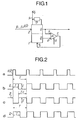
- FIG. 1 schematically represents a circuit for adjusting the duty cycle of a periodic pulse signal, according to the invention.
- This circuit includes a monostable flip-flop 1, which receives on its trigger input 2, an impulse signal of frequency f 0/2 for example, as represented in the diagram a of FIG. 2.
- the adjustment circuit further comprises a comparator constituted by an operational amplifier 4, which receives respectively on its inputs 5, 6, the signals of the direct Q and complementary Q outputs of the monostable flip-flop 1.
- the output of the operational amplifier 4 is connected to the conduction period control input V c of the monostable flip-flop.
- This amplifier also has a control input 8 which, in known manner, makes it possible to adjust the offset voltage of the signals applied to the inputs of the amplifier.
- This adjustment makes it possible, in accordance with the invention, to adjust the duty cycle of the output signals of the monostable flip-flop 1.
- the signals which are used here are those of the direct exit Q of the monostable rocker.
- the monostable flip-flop of this adjustment circuit triggers, as will be seen later, on the rising edges of the pulses received on input 2 of the flip-flop.
- FIG. 2 represents respectively in a, b, c, and d the impulse signals applied to the input 2 of the rocker, the signals collected on the direct outputs Q and complementary Q of this one, in the absence of amplifier operational and the signal collected on the direct output Q when the operational amplifier is present between the outputs of the rocker and its control input of the conduction period V C.
- the operational amplifier 4 whose inputs are connected to the outputs of the monostable flip-flop 1 and whose output is connected to the input V c of this flip-flop, allows, by adjusting the offset voltage of the signals arriving at the input of this amplifier, to adjust the end of the conduction period of the monostable flip-flop and therefore to adjust the duty cycle to signals obtained for example on the direct output Q of the rocker.
- the operational amplifier 4 provides, at the output, a ten error error AV which acts on the duration of conduction of the monostable rocker. The value of this error voltage can be adjusted by an adjustable DC voltage acting on input 8 of the operational amplifier.
- the error voltage in the control loop which includes the operational amplifier 4, results from the comparison of the average value of the direct and complementary signals supplied by the outputs Q and Q of the monostable flip-flop.
- the enslavement achieved is such that the error voltage stabilizes when the duty cycle - of the H / 2 signal obtained on the outputs Q and Q of the rocker, tends towards the value 0.5 for a given setting.
- Any variation in the duty cycle results in an offset of the error voltage which corrects this variation and locks the time constant of the monostable flip-flop over the half-period T of the clock signal H / 2.
- the adjustment which has just been described makes it possible to obtain on the direct output Q, for example, the signal represented on the diagram d of figure 2. On this diagram, is 0.5.
- This adjustment can be made automatically for a range of frequencies whose ratio is of the order of 25. It is obvious that the value of the ratio t is fixed at 0.5 for particular applications, in particular for the use of the circuit cyclic ratio adjustment in a device according to the invention and which makes it possible to multiply by 2 n the frequency of a pulse signal; this ratio can of course be of different value for other applications.
- the conduction time of the monostable rocker is a function of the DC voltage V C applied to the control input of the monostable rocker; this voltage makes it possible to vary the time constant of the monostable rocker in a ratio of up to 25 or 30.
- the operational amplifier delivers a voltage error which is a function of the frequency of the incident signal, and thanks to its large gain ensures that AV is very low, therefore that the duty cycle is very close to 0.5.
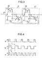
- FIG. 3 represents a frequency multiplier device of a pulse signal, by 2 n .
- This multiplier device includes an adjustment circuit CR identical to that of FIG. 1. The same elements have the same references in this figure and in FIG. 1.
- the duty cycle of the H / 2 clock signals supplied by the CR adjustment circuit is fixed at the value 0.5, as indicated above.
- This adjustment circuit is connected in series with an additional circuit CS, of structure identical to that of the adjustment circuit.
- This additional circuit includes, like the adjustment circuit, a monostable rocker 11 whose tilting input 12 is connected to the direct output Q of the monostable rocker of the adjustment circuit CR.
- a circuit 13 with time constant RC which makes it possible to set the residual conduction duration of the monostable rocker; the control input V makes it possible to vary the conduction time in a ratio 25 to 30.
- This voltage is also chosen so that the latch triggers, on the rising and falling edges, pulses received on the trigger input 12.
- Direct Q 'and complementary outputs Q ' of the flip-flop are respectively connected to the inputs of an operational amplifier 14, the output of which 17 is connected to the control input V of the flip-flop 11.
- the output signals H of the multiplier device are those supplied by the direct output Q '.
- the operational amplifier 14 com takes a control input 18 which makes it possible to adjust the voltage offset of the input signals of this operational amplifier so as to fix the duty cycle of the output signals of this additional circuit.
- FIG. 4 is a diagram of the signals which appear at certain characteristic points of the device of FIG. 3.
- the diagram a represents the clock signals H / 2 applied to the input 2 of flip-flop 1 of the adjustment circuit CR.
- Diagram b represents the signals supplied by the direct output Q of flip-flop 1 of the adjustment circuit.
- flip-flop 1 of this adjustment circuit triggers pulses received at its input on the rising edge and the duty cycle of the signals it delivers at the output has been adjusted so as to be equal to 0 , 5.
- Diagram c represents the signals obtained on the direct output Q ′ of the monostable flip-flop 11 of the additional circuit CS. This flip-flop triggers on the rising and falling edges of the pulses received on its input 12, coming from the output Q of the adjustment circuit.
- the duty cycle , output signals of the flip-flop 11 of the additional circuit CS is equal to 1/2. It is obvious that this cyclical relationship could be different depending on the desired applications of the multiplier device.
- the output Q ′ of the additional circuit CS therefore delivers impulse signals H whose frequency f 0 is twice the frequency f 0/2 of the signals H / 2 received on the input 2 of flip-flop 1 of the adjustment circuit.
- the multiplier device which has just been described makes it possible to double the frequency f 0/2 of H / 2 pulse signals, the frequency of which varies, for example, between 850 kHz and 25 MHz.
- the duty cycle of the output signals from the monostable flip-flop of the additional circuit is set to 0.5, the signals observed are square signals, as shown in diagram c of FIG. 4.
- the distortion of the duty cycle is related to the amplitude of the even harmonics of the device output signal.
- the ratio of the amplitude of the useful signal to the amplitude of the first even harmonic is always greater than 40 decibels.
- the difference in the levels of the output signals and of the monostable flip-flops of the additional adjustment circuits is very easily made up for by adjusting the input offset voltages (offset) of the differential error amplifiers of each circuit.
- This adjustment in the case where the duty cycle of the output signals of the multiplier device must be equal to 0.5, is carried out at the initialization of the system using a spectrum analyzer.
- the delay between the output and the input of the device is of the order of 10 ns.
- the minimum time constant is around 10 ns, the output signal will have a maximum frequency less than or equal to 50 MHz.
- the threshold of the minimum conduction duration of each flip-flop is determined by the user using the time constant circuits 3.13, which allows try to choose the range of variation of time constants.
- the multiplier device which has just been described can be used in digital transmission in particular for bit rates between 2.048 Meb / s. and 34.368 Meb / s., in four-state phase modulation.
Landscapes
- Physics & Mathematics (AREA)
- Nonlinear Science (AREA)
- Pulse Circuits (AREA)
- Manipulation Of Pulses (AREA)
- Stabilization Of Oscillater, Synchronisation, Frequency Synthesizers (AREA)
- Dc Digital Transmission (AREA)
- Networks Using Active Elements (AREA)
Abstract
L'invention concerne un circuit de réglage du rapport cyclique d'un signal périodique impulsionnel. Ce circuit est caractérisé en ce qu'il comprend une bascule monostable (1) qui reçoit le signal impulsionnel sur son entrée de déclenchement (2), un comparateur (4) constitué par un amplificateur opérationnel qui reçoit respectivement sur ses entrées, les signaux de sorties directe (5) et complémentaire (6) de la bascule monostable (1), la sortie (7) de cet amplificateur étant reliée à l'entrée (VC) de commande de la durée de conduction de la bascule monostable (1), cet amplificateur opérationnel (4) comprenant en outre une entrée de commande (8) de la tension de décalage des signaux appliqués à ses entrées, cette entrée de commande permettant de régler le rapport cyclique des signaux de sortie de la bascule (1). Application à la multiplication de fréquence, notamment pour la modulation par déplacement de phases à quatre états.The invention relates to a circuit for adjusting the duty cycle of a periodic pulse signal. This circuit is characterized in that it comprises a monostable flip-flop (1) which receives the impulse signal on its trigger input (2), a comparator (4) constituted by an operational amplifier which receives respectively on its inputs, the signals of direct (5) and complementary (6) outputs of the monostable rocker (1), the output (7) of this amplifier being connected to the input (VC) for controlling the conduction time of the monostable rocker (1), this operational amplifier (4) further comprising a control input (8) for the offset voltage of the signals applied to its inputs, this control input making it possible to adjust the duty cycle of the output signals of the flip-flop (1). Application to frequency multiplication, in particular for modulation by phase displacement with four states.
Description
La présente invention concerne un circuit de réglage du rapport cyclique d'un signal périodique impulsionnel ainsi qu'un dispositif multiplicateur par 2n de la fréquence d'un signal impulsionnel, incluant ce circuit de réglage. Cette invention s'applique à la transmission numérique et notamment à la modulation par déplacement de phases, à quatre états.The present invention relates to a circuit for adjusting the duty cycle of a periodic pulse signal as well as a device multiplying by 2 n the frequency of a pulse signal, including this adjustment circuit. This invention applies to digital transmission and in particular to modulation by phase displacement, with four states.
Pour mieux comprendre l'application de l'invention, notamment à la modulation par déplacement- de phases à quatre états, il est utile de rappeler que dans le domaine de la transmission numérique, le débit d'un signal modulant ou la quantité d'informations transmises par seconde (nombre d'éléments binaires par seconde), est associé à un signal d'horloge ou de rythme H, de fréquence f0. Le signal d'horloge H est un signal rectangulaire de rapport cyclique 0,5. La modulation de phases à quatre états résulte de la composition de deux modulations, par déplacement de phases à deux états, pour lesquelles la fréquence du rythme associé est égale à f 0/2 et est appelée encore horloge H/2. Dans une chaîne de transmission, au niveau du modulateur, le signal modulant est séparé en deux trains numériques A et B dont les débits sont respectivement égaux à la moitié du débit du signal à transmettre. L'horloge associée H/2 est constituée en divisant par deux la fréquence de l'horloge H, généralement à l'aide d'une bascule. A la réception, la démodulation fournit aux erreurs de transmission près, les trains numériques A et B ; elle permet également de retrouver le rythme ou signal d'horloge H/2. Pour reconstituer le signal modulant initial, par entrela- çage, il est nécessaire de reconstituer l'horloge H en doublant la fréquence du rythme de l'horloge H/2.To better understand the application of the invention, in particular to displacement modulation of four-state phases, it is useful to recall that in the field of digital transmission, the rate of a modulating signal or the amount of information transmitted per second (number of binary elements per second), is associated with a clock or rhythm signal H, of frequency f 0 . The clock signal H is a rectangular signal with a duty cycle of 0.5. The four-state phase modulation results from the composition of two modulations, by displacement of two-state phases, for which the frequency of the associated rhythm is equal to f 0/2 and is also called H / 2 clock. In a transmission chain, at the modulator, the modulating signal is separated into two digital trains A and B whose bit rates are respectively equal to half the bit rate of the signal to be transmitted. The associated H / 2 clock is formed by dividing the frequency of the H clock by two, generally using a rocker. On reception, the demodulation supplies, except for transmission errors, the digital trains A and B; it also makes it possible to find the rhythm or clock signal H / 2. To reconstitute the initial modulating signal, by interleaving, it is necessary to reconstitute the H clock by doubling the frequency of the rhythm of the H / 2 clock.
L'invention s'applique particulièrement à la mise en oeuvre de cette dernière opération, c'est-à-dire à la transformation de l'horloge H/2 en horloge H.The invention is particularly applicable to the implementation of this last operation, that is to say that is to say the transformation of the H / 2 clock into an H clock.
Le dispositif multiplicateur de l'invention inclut aussi un circuit de réglage du rapport cyclique d'un signal impulsionnel. On ne connaît pas de dispositif simple qui permette de régler rapidement le rapport cyclique d'un signal périodique impulsionnel et on ne connaît pas non plus de dispositif multiplicateur simple qui permette de multiplier la fréquence d'un signal par deux ou par une puissance n de deux, sans faire intervenir des moyens nombreux, coûteux et difficiles à mettre en oeuvre.The multiplier device of the invention also includes a circuit for adjusting the duty cycle of a pulse signal. There is no known simple device which makes it possible to quickly adjust the duty cycle of a periodic pulse signal, nor is there any known simple multiplier device which makes it possible to multiply the frequency of a signal by two or by a power n of two, without involving numerous means, costly and difficult to implement.
Parmi les dispositifs qui permettent de régler le rapport cyclique d'un signal impulsionnel, le plus simple d'entre eux est constitué par une bascule monostable dont on règle la durée de la période de conduction, en choisissant des valeurs appropriées pour les éléments capacitifs et résistifs qui permettent de fixer la durée de cette période. Ce réglage n'est pas très précis et il est spécifique de la fré- quence du signal.Among the devices which make it possible to adjust the duty cycle of an impulse signal, the simplest of them is constituted by a monostable rocker of which the duration of the conduction period is adjusted, by choosing suitable values for the capacitive elements and resistive which allow to fix the duration of this period. This setting is not very accurate and it is specific to the frequent q uence of the signal.
Les dispositifs doubleurs de fréquence connus sont, soit de type "analogique", soit de type "à boucle de verrouillage de phase".Known frequency doubling devices are either of the "analog" type or of the "phase lock loop" type.
Dans un doubleur de type analogique, le signal d'horloge H/2 de fréquence f0/2 est appliqué au doubleur qui fait apparaître la raie de fréquence double : f0. Il reste à réaliser un filtrage de la raie de fréquence f0 de l'horloge H, puis une amplification suivie d'une remise en forme et d'une remise en phase.In an analog type doubler, the clock signal H / 2 of frequency f 0/2 is applied to the doubler which shows the double frequency line: f 0 . It remains to perform a filtering of the frequency line f 0 of the clock H, then an amplification followed by a reshaping and a reshaping.
Dans le cas d'un dispositif doubleur de fréquence utilisant une boucle à verrouillage de phase, un oscillateur commandé en tension fournit un signal de fréquence f0, double de la fréquence f0/2 de l'horloge H/2. Une comparaison de phases est ensuite effectuée entre le signal incident de fréquence f0/2 et le signal de fréquence f0/2 résultant de la division par deux du signal fourni par l'oscillateur commandé en tension. La tension d'erreur qui résulte de cette comparaison de phases, permet de verrouiller l'oscillateur commandé en tension sur la fréquence f0, en fréquence et en phase. La sortie de l'oscillateur fournit le signal d'horloge H, de fréquence f0.In the case of a frequency doubling device using a phase-locked loop, a voltage-controlled oscillator supplies a signal of frequency f 0 , twice the frequency f 0/2 of the clock H / 2. A phase comparison is then performed killed between the incident signal of frequency f 0/2 and the signal of frequency f 0/2 resulting from the halving of the signal supplied by the voltage-controlled oscillator. The error voltage which results from this phase comparison makes it possible to lock the voltage-controlled oscillator on the frequency f 0 , in frequency and in phase. The output of the oscillator provides the clock signal H, of frequency f 0 .
Le doubleur de fréquence de type analogique comprend donc un filtre passe-bande accordé sur la fréquence f0, un amplificateur de remise en forme et des moyens de remise en phase pour compenser le retard introduit par le filtrage. Ce type de doubleur a pour principal inconvénient d'être spécifique de chaque fréquence liée au débit numérique. De plus, la compensation de la plage d'incertitudes de la fréquence du signal incident est faible ; enfin, pour les débits de faible vitesse, le filtrage doit être étroit pour séparer les raies de fréquence, ce qui augmente le retard à compenser.The analog type frequency doubler therefore comprises a bandpass filter tuned to the frequency f 0 , a fitness amplifier and reshaping means to compensate for the delay introduced by the filtering. The main drawback of this type of doubler is that it is specific to each frequency linked to the digital bit rate. In addition, the compensation of the uncertainty range of the frequency of the incident signal is weak; finally, for low speed flows, the filtering must be tight to separate the frequency lines, which increases the delay to compensate.
Le doubleur de fréquence de type à "boucle de verrouillage de phase" est plus performant. Cependant, la plage d'accrochage et de poursuite de ce doubleur, sur la fréquence du signal d'entrée, est liée au facteur K0 de l'oscillateur commandé en tension. Ce facteur KO est l'excursion de fréquence, couverte par volt de la tension de commande appliquée à l'oscillateur. Avec un oscillateur à quartz, ce facteur K0 est de l'ordre de 10-3 , à 10 . Il en résulte que l'excursion de fréquence est très faible et que ce type de doubleur ne peut être que spécifique à chaque débit d'impulsions à transmettre. Avec un oscillateur classique, la gamme de débit contrôlée peut varier dans un rapport 4 entre le plus faible débit et le plus fort débit. Pour couvrir des plages plus importantes, il est nécessaire de recourir à des montages beaucoup plus complexes qui nécessitent des commutations de gammes.The "phase lock loop" type frequency doubler is more efficient. However, the attachment and tracking range of this doubler, on the frequency of the input signal, is linked to the factor K 0 of the voltage-controlled oscillator. This factor K O is the frequency deviation, covered by volts of the control voltage applied to the oscillator. With a quartz oscillator, this factor K 0 is of the order of 10 -3 , to 10. As a result, the frequency excursion is very small and this type of doubler can only be specific to each pulse rate to be transmitted. With a conventional oscillator, the controlled flow range can vary in a ratio 4 between the lowest flow and the highest flow. To cover larger ranges, it It is necessary to resort to much more complex assemblies which require switching of ranges.
L'invention a pour but de remédier à ces inconvénients et notamment de réaliser un circuit de réglage du rapport cyclique d'un signal périodique impulsionnel, utilisant une bascule monostable dont la période de conduction est commandée, de manière simple, par le réglage de la tension de décalage des signaux appliqués aux entrées d'un amplificateur opéra-. tionnel disposé dans une boucle d'asservissement reliant les sorties de la bascule avec son entrée de contrôle de la période de conduction. Dans le cas de la bascule monostable utilisée, une tension continue appliquée sur cette entrée, permet de faire varier la période de conduction dans un rapport de l'ordre de 30.The object of the invention is to remedy these drawbacks and in particular to produce a circuit for adjusting the duty cycle of a periodic pulse signal, using a monostable rocker whose conduction period is controlled, in a simple manner, by adjusting the offset voltage of the signals applied to the inputs of an operational amplifier. tional disposed in a servo loop connecting the outputs of the scale with its control input of the conduction period. In the case of the monostable rocker used, a direct voltage applied to this input, makes it possible to vary the conduction period in a ratio of the order of 30.
L'invention a aussi pour but de réaliser un dispositif multiplicateur par 2n de la fréquence d'un signal impulsionnel permettant une multiplication de fréquence dans de larges gammes de débits numériques, sans commutation, de conception simple et de réglage facile.The invention also aims to produce a device multiplying by 2 n the frequency of a pulse signal allowing frequency multiplication in wide ranges of digital bit rates, without switching, of simple design and easy adjustment.
L'invention a pour objet un circuit de réglage du rapport cyclique d'un signal périodique impulsionnel, caractérisé en ce qu'il comprend une bascule monostable qui reçoit le signal impulsionnel sur son entrée de déclenchement, un comparateur constitué par un amplificateur opérationnel qui reçoit respectivement sur ses entrées, les signaux des sorties directe et complémentaire de la bascule monostable, la sortie de cet amplificateur étant reliée à l'entrée de commande de la période de conduction de la bascule monostable, cet amplificateur opérationnel comprenant en outre une entrée de commande de la tension de décalage des signaux appliqués à ses entrées, cette entrée de commande permettant de régler le rapport cyclique des signaux de sortie de la bascule, cette bascule déclenchant sur le front montant de chaque impulsion du signal d'entrée.The subject of the invention is a circuit for adjusting the duty cycle of a periodic pulse signal, characterized in that it comprises a monostable flip-flop which receives the pulse signal on its trigger input, a comparator constituted by an operational amplifier which receives respectively on its inputs, the signals of the direct and complementary outputs of the monostable rocker, the output of this amplifier being connected to the control input of the conduction period of the monostable rocker, this operational amplifier further comprising a control input of decaf voltage lage of the signals applied to its inputs, this control input for adjusting the duty cycle of the output signals of the flip-flop, this flip-flop triggering on the rising edge of each pulse of the input signal.
L'invention a aussi pour objet un dispositif multiplicateur par 2n de la fréquence d'un signal impulsionnel, n étant un nombre entier supérieur ou égal à 1, caractérisé par le fait qu'il comprend, selon la valeur de n, l'association en série d'au moins un circuit de réglage de rapport cyclique et d'au moins un circuit supplémentaire de structure identique à celle du circuit de réglage, l'entrée de basculement de la bascule monostable de ce circuit supplémentaire étant reliée à la sortie directe de la bascule monostable du circuit de réglage, la bascule monostable du circuit supplémentaire déclenchant sur les fronts montant et descendant de chaque impulsion reçue sur son entrée, l'amplificateur opérationnel du circuit supplémentaire qui est connecté entre les sorties de la bascule du circuit supplémentaire et l'entrée de commande de la période de conduction de cette bascule, comprenant aussi une entrée de commande de la tension de décalage des signaux appliqués à ses entrées, cette entrée de commande permettant de régler le rapport cyclique des signaux de sortie de la bascule du circuit supplémentaire, le rapport cyclique des signaux de sortie de la bascule du circuit de réglage étant réglé à la valeur 0,5.The invention also relates to a device multiplying by 2 n the frequency of a pulse signal, n being an integer greater than or equal to 1, characterized in that it comprises, depending on the value of n, the series association of at least one duty cycle setting circuit and at least one additional circuit of structure identical to that of the setting circuit, the tilting input of the monostable rocker of this additional circuit being connected to the output direct from the monostable rocker of the adjustment circuit, the monostable rocker of the additional circuit triggering on the rising and falling edges of each pulse received on its input, the operational amplifier of the additional circuit which is connected between the outputs of the rocker of the additional circuit and the input for controlling the conduction period of this flip-flop, also comprising an input for controlling the offset voltage of the signals applied to its inputs, this ent command line for adjusting the duty cycle of the output signals of the flip-flop of the additional circuit, the duty cycle of the output signals of the flip-flop of the adjustment circuit being adjusted to the value 0.5.
Selon une autre caractéristique, le rapport cyclique des signaux de sortie de la bascule du circuit supplémentaire est réglé à la valeur 0,5.According to another characteristic, the duty cycle of the output signals of the flip-flop of the additional circuit is adjusted to the value 0.5.
D'autres caractéristiques et avantages de l'invention ressortiront mieux de la description qui va suivre, donnée en référence aux dessins annexés dans lesquels :
- - la figure 1 représente schématiquement un circuit de réglage du rapport cyclique d'un signal périodique impulsionnel, conforme à l'invention ;
- - la figure 2 est un diagramme des signaux obtenus sur les sorties directe et complémentaire de la bascule monostable de ce circuit de réglage ;
- - la figure 3 représente schématiquement un dispositif multiplicateur de fréquence, conforme à l'invention ;
- - la figure 4 représente -schématiquement un diagramme des signaux apparaissant sur les sorties de certains éléments de ce dispositif.
- - Figure 1 shows schematically a circuit for adjusting the duty cycle of a periodic pulse signal, according to the invention;
- - Figure 2 is a diagram of the signals obtained on the direct and complementary outputs of the monostable rocker of this adjustment circuit;
- - Figure 3 shows schematically a frequency multiplier device, according to the invention;
- - Figure 4 shows -schematically a diagram of the signals appearing on the outputs of certain elements of this device.
La figure 1 représente schématiquement un circuit de réglage du rapport cyclique d'un signal périodique impulsionnel, conforme à l'invention. Ce circuit comprend une bascule monostable 1, qui reçoit sur son entrée de déclenchement 2, un signal impulsionnel de fréquence f0/2 par exemple, tel que représenté sur le diagramme a de la figure 2. On a représenté en 3, de manière schématique, le circuit à résistance/capacité qui permet de fixer la période de conduction résiduelle ou minimum de la bascule monostable. Le circuit de réglage comprend en outre un comparateur constitué par un amplificateur opérationnel 4, qui reçoit respectivement sur ses entrées 5, 6, les signaux des sorties directe Q, et complémentaire Q de la bascule monostable 1. La sortie de l'amplificateur opérationnel 4 est reliée à l'entrée de commande de période de conduction Vc de la bascule monostable. Cet amplificateur présente en outre une entrée de commande 8 qui, de manière connue, permet de régler la tension de décalage des signaux appliqués aux entrées de l'amplificateur. Ce réglage permet, conformément à l'invention, de régler le rapport cyclique des signaux de sortie de la bascule monostable 1. Les signaux qui sont utilisés ici sont ceux de la sortie directe Q de la bascule monostable. La bascule monostable de ce circuit de réglage déclenche, comme on le verra par la suite, sur les fronts montants des impulsions reçues sur l'entrée 2 de la bascule.FIG. 1 schematically represents a circuit for adjusting the duty cycle of a periodic pulse signal, according to the invention. This circuit includes a monostable flip-flop 1, which receives on its
La figure 2 représente respectivement en a, b, c, et d les signaux impulsionnels appliqués à l'entrée 2 de la bascule, les signaux recueillis sur les sorties directe Q et complémentaire Q de celle-ci, en l'absence d'amplificateur opérationnel et le signal recueilli sur la sortie directe Q lorsque l'amplificateur opérationnel est présent entre les sorties de la bascule et son entrée de commande de la période de conduction VC.FIG. 2 represents respectively in a, b, c, and d the impulse signals applied to the
Les impulsions reçues sur l'entrée 2 de la bascule 1 et qui sont représentées sur le diagramme a permettent de déclencher cette bascule sur les fronts montants de ces impulsions et les signaux obtenus sur les sorties directe Q et complémentaire Q de la bascule sont représentés sur les diagrammes b et c. En l'absence d'amplificateur opérationnel entre les sorties de la bascule et l'entrée de commande Vc de celle-ci, le rapport cyclique ![]()
![]()
![]()
![]()
![]()
![]()
Si l'on considère les diagrammes b et c de la figure 2, qui représentent les signaux qui apparaissent sur les sorties directe Q et complémentaire Q de la bascule monostable, lorsque le rapport cyclique de ces signaux est différent de 0,5 et si l'on désigne par E l'amplitude maximale du signal impulsionnel obtenu sur la sortie directe Q de la bascule monostable, la valeur moyenne de ce signal est :![]()
![]()
Dans le cas du diagramme b, V = ![]()
![]()
![]()
![]()
![]()
![]()
![]()
![]()
![]()
![]()
Lorsque le rapport cyclique est égal à 0,5, t = ![]()
![]()
![]()
![]()
La figure 3 représente un dispositif multiplicateur de fréquence d'un signal impulsionnel, par 2 n. Ce dispositif multiplicateur inclut un circuit de réglage CR identique à celui de la figure 1. Les mêmes éléments portent les mêmes références sur cette figure et sur la figure 1. Bien entendu, le rapport cyclique des signaux d'horloge H/2 fournis par le circuit de réglage de CR, est fixé à la valeur 0,5, comme on l'a indiqué plus haut. Ce circuit de réglage est connecté en série avec un circuit supplémentaire CS, de structure identique à celle du circuit de réglage. Ce circuit supplémentaire comprend, comme le circuit de réglage, une bascule monostable 11 dont l'entrée de basculement 12 est reliée à la sortie directe Q de la bascule monostable du circuit de réglage CR. On a également représenté sur cette figure un circuit 13 à constante de temps RC, qui permet de fixer la durée de conduction résiduelle de la bascule monostable ; l'entrée de commande V permet de faire varier la durée de conduction dans un rapport 25 à 30. Cette tension est également choisie pour que la bascule déclenche, sur les fronts montant et descendant, des impulsions reçues sur l'entrée de déclenchement 12. Les sorties directe Q' et complémentaire
La figure 4 est un diagramme des signaux qui apparaissent en certains points caractéristiques du dispositif de la figure 3. Le diagramme a représente les signaux d'horloge H/2 appliqués à l'entrée 2 de la bascule 1 du circuit de réglage CR. Le diagramme b représente les signaux fournis par la sortie directe Q de la bascule 1 du circuit de réglage.FIG. 4 is a diagram of the signals which appear at certain characteristic points of the device of FIG. 3. The diagram a represents the clock signals H / 2 applied to the
Comme on l'a mentionné plus haut, la bascule 1 de ce circuit de réglage déclenche sur le front montant des impulsions reçues sur son entrée et le rapport cyclique des signaux qu'elle délivre en sortie a été réglé de manière à être égal à 0,5. Le diagramme c représente les signaux obtenus sur la sortie directe Q' de la bascule monostable 11 du circuit supplémentaire CS. Cette bascule déclenche sur les fronts montant et descendant des impulsions reçues sur son entrée 12, en provenance de la sortie Q du circuit de réglage. Dans un mode particulier de réglage, qui correspond au diagramme c de la figure, le rapport cycli- que ![]()
![]()
![]()
![]()
Dans le dispositif multiplicateur de fréquence qui vient d'être décrit, il est possible d'associer en série avec le circuit supplémentaire, d'autres circuits supplémentaires identiques et dont le rapport cyclique des signaux de sortie est réglé à la valeur 0,5, de manière à former un dispositif multiplicateur par 2n. La valeur de n dépend bien entendu du nombre de circuits supplémentaires associés au dispositif précédemment décrit.In the frequency multiplier device which has just been described, it is possible to as combine in series with the additional circuit, other identical additional circuits whose cyclic ratio of the output signals is set to the value 0.5, so as to form a multiplier by 2 n . The value of n naturally depends on the number of additional circuits associated with the device described above.
Le dispositif multiplicateur qui vient d'être décrit permet de doubler la fréquence f 0/2 de signaux impulsionnels H/2, dont la fréquence varie, par exemple, entre 850 kHz et 25 MHz. Lorsque le rapport cyclique des signaux de sortie de la bascule monostable du circuit supplémentaire est réglé à la valeur 0,5, les signaux observés sont des signaux carrés, tels que représentés sur le diagramme c de la figure 4. La distorsion du rapport cyclique est liée à l'amplitude des harmoniques pairs du signal de sortie du dispositif. Le rapport de l'amplitude du signal utile à l'amplitude du premier harmonique pair est toujours supérieur à 40 décibels. L'écart des niveaux des signaux de sortie et des bascules monostables des circuits de réglage supplémentaire, est très facilement rattrapé par le réglage des tensions de décalage d'entrées (offset) des amplificateurs différentiels d'erreur de chaque circuit. Ce réglage, dans le cas où le rapport cyclique des signaux de sortie du dispositif multiplicateur doit être égal à 0,5, est effectué à l'initialisation du système à l'aide d'un analyseur de spectre. Le retard entre la sortie et l'entrée du dispositif est de l'ordre de 10 ns. La constante de temps minimum est de l'ordre 10 ns, le signal de sortie aura une fréquence maximum inférieure ou égale à 50 MHz. Le seuil de la durée de conduction minimum de chaque bascule est déterminé par l'utilisateur à l'aide des circuits à constante de temps 3,13, qui permettent de choisir la gamme de variation des constantes de temps. Il est ainsi possible, grâce à ces réglages, d'utiliser le dispositif dans une large gamme de fréquence ; lorsque les réglages initiaux ont été effectués, les boucles d'asservissement apportent une auto- compensation des défauts si le gain de chaque boucle est suffisant. Lorsque seul le circuit de réglage du rapport cyclique est utilisé, ce rapport cyclique peut varier entre 0,1 et 0,9 grâce au réglage de la tension d'offset de l'amplificateur opérationnel 4. Pour un réglage donné, il est possible d'obtenir un rapport cyclique fixe dans toute la gamme des fréquences.The multiplier device which has just been described makes it possible to double the frequency f 0/2 of H / 2 pulse signals, the frequency of which varies, for example, between 850 kHz and 25 MHz. When the duty cycle of the output signals from the monostable flip-flop of the additional circuit is set to 0.5, the signals observed are square signals, as shown in diagram c of FIG. 4. The distortion of the duty cycle is related to the amplitude of the even harmonics of the device output signal. The ratio of the amplitude of the useful signal to the amplitude of the first even harmonic is always greater than 40 decibels. The difference in the levels of the output signals and of the monostable flip-flops of the additional adjustment circuits is very easily made up for by adjusting the input offset voltages (offset) of the differential error amplifiers of each circuit. This adjustment, in the case where the duty cycle of the output signals of the multiplier device must be equal to 0.5, is carried out at the initialization of the system using a spectrum analyzer. The delay between the output and the input of the device is of the order of 10 ns. The minimum time constant is around 10 ns, the output signal will have a maximum frequency less than or equal to 50 MHz. The threshold of the minimum conduction duration of each flip-flop is determined by the user using the time constant circuits 3.13, which allows try to choose the range of variation of time constants. It is thus possible, thanks to these settings, to use the device in a wide frequency range; when the initial settings have been made, the control loops provide self-compensation for faults if the gain of each loop is sufficient. When only the duty cycle setting circuit is used, this duty cycle can vary between 0.1 and 0.9 thanks to the adjustment of the offset voltage of the operational amplifier 4. For a given setting, it is possible to '' obtain a fixed duty cycle over the entire frequency range.
Le dispositif multiplicateur qui vient d'être décrit peut être utilisé en transmission numérique notamment pour des débits compris entre 2,048 Meb/s. et 34,368 Meb/s., en modulation de phase à quatre états.The multiplier device which has just been described can be used in digital transmission in particular for bit rates between 2.048 Meb / s. and 34.368 Meb / s., in four-state phase modulation.
Claims (3)
Applications Claiming Priority (2)
| Application Number | Priority Date | Filing Date | Title |
|---|---|---|---|
| FR8027670 | 1980-12-29 | ||
| FR8027670A FR2497427A1 (en) | 1980-12-29 | 1980-12-29 | CIRCUIT FOR ADJUSTING THE CYCLIC RATIO OF AN IMPULSE PERIODIC SIGNAL AND FREQUENCY MULTIPLIER DEVICE BY 2, INCLUDING THE ADJUSTING CIRCUIT |
Publications (3)
| Publication Number | Publication Date |
|---|---|
| EP0055670A2 true EP0055670A2 (en) | 1982-07-07 |
| EP0055670A3 EP0055670A3 (en) | 1982-08-04 |
| EP0055670B1 EP0055670B1 (en) | 1985-05-22 |
Family
ID=9249557
Family Applications (1)
| Application Number | Title | Priority Date | Filing Date |
|---|---|---|---|
| EP81402071A Expired EP0055670B1 (en) | 1980-12-29 | 1981-12-23 | Duty cycle control circuit for a periodic pulse signal, and 2n frequency multiplier including this circuit |
Country Status (7)
| Country | Link |
|---|---|
| US (1) | US4439689A (en) |
| EP (1) | EP0055670B1 (en) |
| JP (1) | JPS57133743A (en) |
| AU (1) | AU550255B2 (en) |
| CA (1) | CA1177909A (en) |
| DE (1) | DE3170659D1 (en) |
| FR (1) | FR2497427A1 (en) |
Cited By (1)
| Publication number | Priority date | Publication date | Assignee | Title |
|---|---|---|---|---|
| WO1997023955A1 (en) * | 1995-12-22 | 1997-07-03 | Thomson Consumer Electronics, Inc. | Voltage controlled crystal oscillator and loop filter |
Families Citing this family (9)
| Publication number | Priority date | Publication date | Assignee | Title |
|---|---|---|---|---|
| US4527075A (en) * | 1983-07-11 | 1985-07-02 | Sperry Corporation | Clock source with automatic duty cycle correction |
| US4596954A (en) * | 1984-02-29 | 1986-06-24 | American Microsystems, Inc. | Frequency doubler with fifty percent duty cycle output signal |
| IT1204915B (en) * | 1987-03-11 | 1989-03-10 | Montedison Spa | DERIVATORS FOR ASYNCHRONOUS SYSTEMS |
| US5008636A (en) * | 1988-10-28 | 1991-04-16 | Apollo Computer, Inc. | Apparatus for low skew system clock distribution and generation of 2X frequency clocks |
| DE4020977A1 (en) * | 1990-07-02 | 1992-01-16 | Broadcast Television Syst | CIRCUIT ARRANGEMENT FOR GENERATING A SYMMETRICAL PULSE SIGNAL |
| DE19822373C2 (en) * | 1998-02-20 | 2001-05-31 | Ind Technology Res Inst Hsinch | Frequency multiplication circuit and method |
| DE102005051814A1 (en) * | 2005-10-28 | 2007-05-03 | Infineon Technologies Ag | Electronic test apparatus e.g. for testing circuits, has clock signal generator and driver having several subunits each generating phase-shifted driver signal in response to clock signal |
| US8314639B2 (en) | 2010-03-24 | 2012-11-20 | Mediatek Inc. | Frequency divider for generating output clock signal with duty cycle different from duty cycle of input clock signal |
| CN111106817B (en) * | 2018-10-09 | 2023-04-25 | 中车株洲电力机车研究所有限公司 | Signal delay circuit |
Citations (1)
| Publication number | Priority date | Publication date | Assignee | Title |
|---|---|---|---|---|
| US3646370A (en) * | 1970-07-06 | 1972-02-29 | Honeywell Inc | Stabilized monostable delay multivibrator or one-shot apparatus |
Family Cites Families (5)
| Publication number | Priority date | Publication date | Assignee | Title |
|---|---|---|---|---|
| JPS5039983B2 (en) * | 1971-12-23 | 1975-12-20 | ||
| US3820029A (en) * | 1973-05-15 | 1974-06-25 | Halliburton Co | Precision voltage control monostable multivibrator |
| JPS52111359A (en) * | 1976-03-16 | 1977-09-19 | Mitsubishi Electric Corp | Pulse-width controller |
| JPS54150452U (en) * | 1978-04-11 | 1979-10-19 | ||
| US4277697A (en) * | 1979-01-15 | 1981-07-07 | Norlin Industries, Inc. | Duty cycle control apparatus |
-
1980
- 1980-12-29 FR FR8027670A patent/FR2497427A1/en active Granted
-
1981
- 1981-12-09 US US06/328,806 patent/US4439689A/en not_active Expired - Lifetime
- 1981-12-15 CA CA000392307A patent/CA1177909A/en not_active Expired
- 1981-12-18 AU AU78631/81A patent/AU550255B2/en not_active Expired
- 1981-12-23 EP EP81402071A patent/EP0055670B1/en not_active Expired
- 1981-12-23 JP JP56216065A patent/JPS57133743A/en active Granted
- 1981-12-23 DE DE8181402071T patent/DE3170659D1/en not_active Expired
Patent Citations (2)
| Publication number | Priority date | Publication date | Assignee | Title |
|---|---|---|---|---|
| US3646370A (en) * | 1970-07-06 | 1972-02-29 | Honeywell Inc | Stabilized monostable delay multivibrator or one-shot apparatus |
| FR2100225A5 (en) * | 1970-07-06 | 1972-03-17 | Honeywell Inc |
Non-Patent Citations (4)
| Title |
|---|
| EDN Electrical Design News, Vol. 23, No. 14, 5 Aout 1978 Denver, US P.A. LAWLESS: "One-Shot Forms Frequency Multiplier", page 72 *page 72, partie Inferieure* * |
| Electronics, Vol. 48, No. 15, 24 Juillet 1975 New York, US H.P.D. LANYON: "One-Shot with Feedback Loop Maintains Constant Duty Cycle", pages 93-95 *figure; pages 93 et 95, partie Superieure* * |
| Electronics, Vol. 49, No. 15, 22 Juillet 1976 New York, US R.L. TAYLOR: "Frequency-Doubler Produces Square-Wave Output", pages 111 et 113. *figure 2; page 113, colonne de gauche, dernier alinea - colonne de droite* * |
| The Electronic Engineer, Vol. 30, No. 1, Janvier 1971 Radnor, US K. ERICKSON: "One-Shot Triggers on Both Edges of Input", page 45 *page 45, partie Inferieure* * |
Cited By (1)
| Publication number | Priority date | Publication date | Assignee | Title |
|---|---|---|---|---|
| WO1997023955A1 (en) * | 1995-12-22 | 1997-07-03 | Thomson Consumer Electronics, Inc. | Voltage controlled crystal oscillator and loop filter |
Also Published As
| Publication number | Publication date |
|---|---|
| JPH0442851B2 (en) | 1992-07-14 |
| EP0055670A3 (en) | 1982-08-04 |
| AU550255B2 (en) | 1986-03-13 |
| FR2497427B1 (en) | 1985-02-15 |
| CA1177909A (en) | 1984-11-13 |
| US4439689A (en) | 1984-03-27 |
| DE3170659D1 (en) | 1985-06-27 |
| FR2497427A1 (en) | 1982-07-02 |
| AU7863181A (en) | 1982-07-08 |
| EP0055670B1 (en) | 1985-05-22 |
| JPS57133743A (en) | 1982-08-18 |
Similar Documents
| Publication | Publication Date | Title |
|---|---|---|
| FR2473816A1 (en) | LOOP LOCKING SYSTEM | |
| FR2523388A1 (en) | ADAPTIVE THRESHOLD DEVICE | |
| FR2633467A1 (en) | FREQUENCY MULTIPLIER WITH PROGRAMMABLE MULTIPLICATION RANK | |
| FR2622751A1 (en) | MODULATOR / DEMODULATOR CIRCUIT AND INSULATION AMPLIFIER EMPLOYING THIS CIRCUIT | |
| EP0055670B1 (en) | Duty cycle control circuit for a periodic pulse signal, and 2n frequency multiplier including this circuit | |
| EP0125979A1 (en) | Demodulator for constant envelope and continuous phase signals angularly modulated by a series of binary symbols | |
| EP0667677A1 (en) | Device for multiplying a capacitance by a variable coefficient for adjusting a filter cut-off frequency and filter comprising same | |
| EP0564377A1 (en) | Frequency locked loop | |
| FR2530898A1 (en) | PHASE LOCKED LOOP TUNING DEVICE | |
| FR2615677A1 (en) | DIGITAL PHASE LOCKOUT LOOP CIRCUIT | |
| EP1101316B1 (en) | Clock recovery method in digital signal sampling | |
| FR2503498A1 (en) | TRANSMITTER FOR ANGULAR-MODULATING SIGNALS | |
| EP0042641B1 (en) | Frequency demodulator using a delay circuit, the delay of which varies according to the received frequency | |
| FR2552955A1 (en) | METHOD FOR CONTROLLING THE FREQUENCY OF AN OSCILLATOR AND A CONTROL CIRCUIT WITH A PHASE-STACKING LOOP | |
| FR2542529A1 (en) | LINEAR INTERPOLATION PULSE NOISE REDUCTION CIRCUIT WITH WHITE NOISE INSENSITIVITY | |
| EP0121750A1 (en) | Clock recovery circuit for a synchronous data transmission utilizing a combination of the biphase L code, and the modified biphase code | |
| EP0092879B1 (en) | Bit synchronisation device for a data transmission modulator-demodulator or receiver | |
| EP0174237B1 (en) | Device for the fast clock and phase acquisition of a digital signal | |
| EP0624954B1 (en) | Arrangement for reducing the spurious spectral lines contained in a digital frequency synthesizer output signal | |
| FR2462816A1 (en) | Carrier waveform phase modulation and prefiltering - provides data transmission with good carrier recovery with multiplexer controlled by counter | |
| FR2568738A1 (en) | Device for recovering the clock signal in a digital transmission | |
| EP0645892B1 (en) | Frequency-locked loop | |
| EP0086140A1 (en) | High stability voltage-frequency converter | |
| FR2567702A1 (en) | Constant-current transmitter for transmitting data over a transmission line | |
| EP0026372A1 (en) | Local oscillator phase control circuit for a receiver of data signals transmitted by single side-band amplitude modulation |
Legal Events
| Date | Code | Title | Description |
|---|---|---|---|
| PUAI | Public reference made under article 153(3) epc to a published international application that has entered the european phase |
Free format text: ORIGINAL CODE: 0009012 |
|
| PUAL | Search report despatched |
Free format text: ORIGINAL CODE: 0009013 |
|
| AK | Designated contracting states |
Designated state(s): DE GB NL |
|
| AK | Designated contracting states |
Designated state(s): DE GB NL |
|
| 17P | Request for examination filed |
Effective date: 19821204 |
|
| GRAA | (expected) grant |
Free format text: ORIGINAL CODE: 0009210 |
|
| AK | Designated contracting states |
Designated state(s): DE GB NL |
|
| REF | Corresponds to: |
Ref document number: 3170659 Country of ref document: DE Date of ref document: 19850627 |
|
| PLBE | No opposition filed within time limit |
Free format text: ORIGINAL CODE: 0009261 |
|
| STAA | Information on the status of an ep patent application or granted ep patent |
Free format text: STATUS: NO OPPOSITION FILED WITHIN TIME LIMIT |
|
| 26N | No opposition filed | ||
| PGFP | Annual fee paid to national office [announced via postgrant information from national office to epo] |
Ref country code: GB Payment date: 20001129 Year of fee payment: 20 |
|
| PGFP | Annual fee paid to national office [announced via postgrant information from national office to epo] |
Ref country code: DE Payment date: 20001206 Year of fee payment: 20 |
|
| PGFP | Annual fee paid to national office [announced via postgrant information from national office to epo] |
Ref country code: NL Payment date: 20001207 Year of fee payment: 20 |
|
| PG25 | Lapsed in a contracting state [announced via postgrant information from national office to epo] |
Ref country code: GB Free format text: LAPSE BECAUSE OF EXPIRATION OF PROTECTION Effective date: 20011222 |
|
| PG25 | Lapsed in a contracting state [announced via postgrant information from national office to epo] |
Ref country code: NL Free format text: LAPSE BECAUSE OF EXPIRATION OF PROTECTION Effective date: 20011223 |
|
| REG | Reference to a national code |
Ref country code: GB Ref legal event code: PE20 Effective date: 20011222 |
|
| NLV7 | Nl: ceased due to reaching the maximum lifetime of a patent |
Effective date: 20011223 |