EP0055573B1 - Komparator-Schaltkreis - Google Patents
Komparator-Schaltkreis Download PDFInfo
- Publication number
- EP0055573B1 EP0055573B1 EP81305985A EP81305985A EP0055573B1 EP 0055573 B1 EP0055573 B1 EP 0055573B1 EP 81305985 A EP81305985 A EP 81305985A EP 81305985 A EP81305985 A EP 81305985A EP 0055573 B1 EP0055573 B1 EP 0055573B1
- Authority
- EP
- European Patent Office
- Prior art keywords
- terminal
- level
- voltage
- input
- level shift
- Prior art date
- Legal status (The legal status is an assumption and is not a legal conclusion. Google has not performed a legal analysis and makes no representation as to the accuracy of the status listed.)
- Expired
Links
Images

Classifications
-
- H—ELECTRICITY
- H03—ELECTRONIC CIRCUITRY
- H03K—PULSE TECHNIQUE
- H03K3/00—Circuits for generating electric pulses; Monostable, bistable or multistable circuits
- H03K3/02—Generators characterised by the type of circuit or by the means used for producing pulses
- H03K3/023—Generators characterised by the type of circuit or by the means used for producing pulses by the use of differential amplifiers or comparators, with internal or external positive feedback
- H03K3/0233—Bistable circuits
- H03K3/02337—Bistables with hysteresis, e.g. Schmitt trigger
-
- H—ELECTRICITY
- H03—ELECTRONIC CIRCUITRY
- H03K—PULSE TECHNIQUE
- H03K3/00—Circuits for generating electric pulses; Monostable, bistable or multistable circuits
- H03K3/02—Generators characterised by the type of circuit or by the means used for producing pulses
- H03K3/023—Generators characterised by the type of circuit or by the means used for producing pulses by the use of differential amplifiers or comparators, with internal or external positive feedback
Definitions
- This invention relates to a comparator circuit.
- the hysteresis width is determined normally in dependence upon power supply voltage and resistance ratio.
- the power supply voltage is usually comparatively constant but in some cases changes considerably.
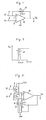
- Figure 1 shows the structure of an existing ordinary comparator circuit.
- 10 is a high gain differential amplifier having an input terminal (positive side) 1, reference terminal 2 (negative side) and output terminal 3, and its input terminal 1 is connected to the input voltage terminal 4, while the reference terminal 2 is connected to the reference voltage terminal 5.
- V an input voltage
- V r an input voltage
- V 1 (1) ⁇ V r (2) where V,(1) is an input voltage at the input terminal 1 and V R (2) is the reference voltage at the reference terminal 2
- the differential amplifier 10 outputs an output voltage V o of L (low) level to the output terminal 3, and when V i (1)>V r (2), an output voltage V o of H (high) level is provided.
- the hysteresis width W of the comparator circuit having such hysteresis characteristic is influenced by the power supply voltage V cc .
- the H level output voltage V o is determined by the power supply voltage V cc and becomes small when the power supply voltage is lowered. Therefore, the circuit shown in Fig. 1 has a disadvantage that a value of input voltage V I (4) which changes from H level to L or from L level to H causes the hysteresis width W to change also.
- a preferred embodiment of the present invention provides a comparator circuit which does not allow the hysteresis width to change due to a change of power supply voltage.
- a preferred embodiment moreover provides a comparator circuit which is capable of sustaining a constant hysteresis width without requiring a change of constant of external elements even when the power supply voltage or power source current is change in the range of several times rated value.
- a comparator circuit operatively connected to receive input and reference voltages and comprising:
- first level shift means operatively connected between said input voltage terminal and said input terminal, or between said reference voltage terminal and said reference terminal, for shifting the level of the input voltage or the reference voltage to provide hysteresis which is substantially independent of power supply voltage; said first level shift means comprising a diode or a base-emitter path of a transistor;
- first current source means operatively connected to said first level shift means for supplying current to said first level shift means; and control means operatively connected to said first current source means and said output terminal for controlling the current value of said current source means in accordance with the output level of said output terminal.
- the emitter follower type transistors Q 1 , Q 2 are driven by a constant current by the current sources 8, 9 so that an input current can be ignored. These currents 1 1 , 1 2 are given by the following equations.
- V BE1' V BE2 are the base emitter voltage of transistors Q 1 , Q 2 .
- the current source 9 outputs ml 1 and V BE2 becomes large as is obvious from the equation (4) (increment is considered as ⁇ V).
- the reference voltage V r is supposed to be lowered by ⁇ V when considered from the differential amplifier 10. Therefore, a voltage being input to the input terminal 1 of the differential amplifier 10 seems to be relatively increased. For this reason, when an output voltage V o . returns to the L level, an input voltage V 1 must be lowered by ⁇ V than the reference voltage V r and thereby an output voltage V o indicates the hysteresis characteristic having the width of ⁇ V.
- the width ⁇ V depends on the physical constants such as k, T, q and a current ratio of l 2 /l 1 but not on the power supply voltage V cc .
- the hysteresis width thus obtained is not influenced by power supply voltage fluctuation.
- resistance values fluctuate considerably but a current ratio of the constant current source can be set accurately to the desired value. Resultingly, the hysteresis width can be adjusted accurately by changing such current ratio.
- the current source 8 in the input voltage V 1 side is increased in the backward direction together with the current source 9, namely when 1 2 is increased m times, the hysteresis width is doubled compared to that while only one current source is used by changing 1 1 to I/m.
- the level shift means 6 and current source 8 can be omitted.
- an input voltage V i is directly applied to the input terminal 1 (without level shift) and therefore when V i >V r ⁇ V BE2 , an output voltage V o turns to the H level from L level.
- the hysteresis characteristic can be obtained by controlling a constant current value of the current source 8 or 9.
- Figure 4 shows the structure of a comparator circuit according to another embodiment of the present invention.
- Figure 5 shows the structure of a comparator circuit according to another embodiment of the present invention.
- a current value of the constant current source can be done easily, for example, by changing over the two current sources of l 1 , ml 1 prepared with the H and L levels of the output voltage V o .
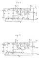
- Figure 6 is an example of a practical circuit corresponding to an embodiment of Fig. 3.
- the transistors Q 101 to Q 103 , Q 3 , Q 4 and Q 7 correspond to the differential amplifier 10, and Q 1' Q 2 are input transistors, while Q 6 , Q 8 , Q 11 are current source transistor and these respectively correspond to said level shift means 6, 7 and current sources 8, 9.
- the transistors Q 104 to Q 106 control the circuit for generating the bias current l o , while the transistors Q 5 , Q 9 , Q 10 control the bias current of differential amplifier 10 with said current.
- the transistor Q 9 is OFF, and resultingly the bias current 1 1 of transistor Q 1 is two times of l o and the bias current 1 2 of transistor Q 2 is equal to l o . Therefore, V BE of transistor Q 1 and V BE of transistor Q 2 are in the following relation.
- Figure 7 shows another practical example. This circuit is different from Fig. 6 in that the current source transistors Q 6 , Q 8 are omitted.
- the base current of transistors Q 3 , Q 4 in the next stage is used as the bias current of level shift means 6, and therefore the hysteresis width ⁇ W becomes as follows:
- ⁇ is the current amplification coefficient of the NPN transistors Q 3 , Q 4 .
- ⁇ W 120 to 160mV, resulting in a large hysteresis width. Therefore, the circuit of Fig. 7 is a very effective circuit for a certain purpose.
- a comparator circuit having a hysteresis characteristic of accurate width which is not influenced by fluctuation of power source voltage is obtained by the method that the input voltage V, and/or the reference voltage V r is shifted by V BE of a transistor and said V BE is changed in accordance with the output level of the comparator circuit.
Landscapes
- Manipulation Of Pulses (AREA)
- Measurement Of Current Or Voltage (AREA)
Claims (2)
gekennzeichnet durch
Applications Claiming Priority (2)
| Application Number | Priority Date | Filing Date | Title |
|---|---|---|---|
| JP188936/80 | 1980-12-26 | ||
| JP55188936A JPS57111116A (en) | 1980-12-26 | 1980-12-26 | Comparator having hysteresis |
Publications (2)
| Publication Number | Publication Date |
|---|---|
| EP0055573A1 EP0055573A1 (de) | 1982-07-07 |
| EP0055573B1 true EP0055573B1 (de) | 1985-06-19 |
Family
ID=16232484
Family Applications (1)
| Application Number | Title | Priority Date | Filing Date |
|---|---|---|---|
| EP81305985A Expired EP0055573B1 (de) | 1980-12-26 | 1981-12-21 | Komparator-Schaltkreis |
Country Status (5)
| Country | Link |
|---|---|
| US (1) | US4456840A (de) |
| EP (1) | EP0055573B1 (de) |
| JP (1) | JPS57111116A (de) |
| DE (1) | DE3171073D1 (de) |
| IE (1) | IE52374B1 (de) |
Families Citing this family (22)
| Publication number | Priority date | Publication date | Assignee | Title |
|---|---|---|---|---|
| CA1203290A (en) * | 1982-04-28 | 1986-04-15 | Yoshio Shimizu | Signal comparing circuit |
| JPS59110220A (ja) * | 1982-12-15 | 1984-06-26 | Matsushita Electric Ind Co Ltd | シユミツト回路 |
| US4647796A (en) * | 1983-04-25 | 1987-03-03 | Fairchild Semiconductor Corporation | Multiple level voltage comparator circuit |
| US4581545A (en) * | 1983-10-04 | 1986-04-08 | At&T Technologies | Schmitt trigger circuit |
| JPH063868B2 (ja) * | 1984-09-29 | 1994-01-12 | 株式会社東芝 | 差動型コンパレ−タ回路 |
| JPS61120515A (ja) * | 1984-11-15 | 1986-06-07 | Nec Corp | ヒステリシス回路 |
| KR910009557B1 (ko) * | 1987-03-31 | 1991-11-21 | 미쓰비시 뎅끼 가부시끼가이샤 | 동기신호 처리회로 |
| JPH01138467A (ja) * | 1987-11-25 | 1989-05-31 | Mitsubishi Electric Corp | 電圧比較器 |
| US4945229A (en) * | 1988-12-29 | 1990-07-31 | Thomas & Betts Corporation | Fiber optic receiver and transceiver |
| US5030856A (en) * | 1989-05-04 | 1991-07-09 | International Business Machines Corporation | Receiver and level converter circuit with dual feedback |
| JP2607729B2 (ja) * | 1990-04-21 | 1997-05-07 | 株式会社東芝 | ヒステリシスコンパレータ |
| DE4030085A1 (de) * | 1990-09-22 | 1992-03-26 | Philips Patentverwaltung | Auswerteschaltung fuer einen magnetoresistiven drehzahlsensor o. dgl. |
| JP2731057B2 (ja) * | 1991-11-12 | 1998-03-25 | 川崎製鉄株式会社 | コンパレータ |
| JPH06104704A (ja) * | 1992-09-18 | 1994-04-15 | Mitsubishi Electric Corp | 半導体集積回路装置の入力回路 |
| JP2586785B2 (ja) * | 1993-02-01 | 1997-03-05 | 日本電気株式会社 | 信号レベル変換回路 |
| JP2734963B2 (ja) * | 1993-12-28 | 1998-04-02 | 日本電気株式会社 | 低電圧コンパレータ回路 |
| US5682392A (en) * | 1994-09-28 | 1997-10-28 | Teradyne, Inc. | Method and apparatus for the automatic generation of boundary scan description language files |
| US5587674A (en) * | 1994-12-30 | 1996-12-24 | Sgs-Thomson Microelectronics, Inc. | Comparator with built-in hysteresis |
| AT412600B (de) * | 1996-10-29 | 2005-04-25 | Bernhard Dipl Ing Rzepa | Schaltungsanordnung zur hysteresebehafteten schwellwertdetektion des spitzenwertes eines periodischen eingangssignales |
| US6181187B1 (en) * | 1999-09-30 | 2001-01-30 | Texas Instruments Incorporated | Circuit for auto-centering control loop bias currents |
| DE10221088A1 (de) * | 2002-05-11 | 2003-11-27 | Braun Gmbh | Elektronische Schaltung mit mindestens einem Eingang zum Wählen eines Zustands der elektronischen Schaltung |
| US6956410B2 (en) * | 2003-11-13 | 2005-10-18 | Delphi Technologies, Inc. | Automotive ignition system with battery dependent over-dwell protection |
Family Cites Families (10)
| Publication number | Priority date | Publication date | Assignee | Title |
|---|---|---|---|---|
| US3569739A (en) * | 1967-12-18 | 1971-03-09 | Bendix Corp | Variable level detector network having constant percentage hysteresis |
| US3890575A (en) * | 1969-07-17 | 1975-06-17 | Bendix Corp | Window trip monitor and comparator circuit |
| US3628059A (en) * | 1970-06-01 | 1971-12-14 | Fairchild Camera Instr Co | High voltage functional comparator |
| US3673508A (en) * | 1970-08-10 | 1972-06-27 | Texas Instruments Inc | Solid state operational amplifier |
| US3760195A (en) * | 1972-08-28 | 1973-09-18 | Bell Canada Northern Electric | Trigger comparator circuit |
| US3816761A (en) * | 1973-01-02 | 1974-06-11 | Rca Corp | Comparator circuitry |
| US3848139A (en) * | 1973-09-14 | 1974-11-12 | Fairchild Camera Instr Co | High-gain comparator circuit |
| US4114149A (en) * | 1976-07-19 | 1978-09-12 | Fairchild Camera And Instrument Corporation | Current comparator for an improved analog-to-digital converter method and apparatus |
| DE2833996C2 (de) * | 1978-08-03 | 1984-12-13 | Robert Bosch Gmbh, 7000 Stuttgart | Transistorverstärker |
| JPS5674661A (en) * | 1979-11-24 | 1981-06-20 | Fujitsu Ltd | Differential amplifier |
-
1980
- 1980-12-26 JP JP55188936A patent/JPS57111116A/ja active Pending
-
1981
- 1981-12-11 US US06/329,947 patent/US4456840A/en not_active Expired - Fee Related
- 1981-12-21 EP EP81305985A patent/EP0055573B1/de not_active Expired
- 1981-12-21 DE DE8181305985T patent/DE3171073D1/de not_active Expired
- 1981-12-23 IE IE3066/81A patent/IE52374B1/en not_active IP Right Cessation
Also Published As
| Publication number | Publication date |
|---|---|
| DE3171073D1 (en) | 1985-07-25 |
| EP0055573A1 (de) | 1982-07-07 |
| JPS57111116A (en) | 1982-07-10 |
| IE52374B1 (en) | 1987-09-30 |
| IE813066L (en) | 1982-06-26 |
| US4456840A (en) | 1984-06-26 |
Similar Documents
| Publication | Publication Date | Title |
|---|---|---|
| EP0055573B1 (de) | Komparator-Schaltkreis | |
| US4352056A (en) | Solid-state voltage reference providing a regulated voltage having a high magnitude | |
| TWI859269B (zh) | 參考電壓電路 | |
| US4099115A (en) | Constant-voltage regulated power supply | |
| EP0039178B1 (de) | Integrierte Schaltung zum Erzeugen einer Referenzspannung | |
| EP0139425B1 (de) | Konstanter Stromquellenkreis | |
| US4268789A (en) | Limiter circuit | |
| US4658205A (en) | Reference voltage generating circuit | |
| US4677368A (en) | Precision thermal current source | |
| US4556805A (en) | Comparator circuit having hysteresis voltage substantially independent of variation in power supply voltage | |
| US4219781A (en) | Transistor amplifier circuit | |
| US3947704A (en) | Low resistance microcurrent regulated current source | |
| US4644257A (en) | Band gap circuit | |
| US4686395A (en) | Current switching type logic circuit | |
| US4675593A (en) | Voltage power source circuit with constant voltage output | |
| EP0530500A1 (de) | Stromspiegelschaltung | |
| EP0411657B1 (de) | Konstantspannungsschaltung | |
| US4177417A (en) | Reference circuit for providing a plurality of regulated currents having desired temperature characteristics | |
| EP0182201B1 (de) | Geschwindigkeitsregelgerät für einen Gleichstrommotor | |
| EP0007804B1 (de) | Stabilisierender Vorspannungskreis mit einer bestimmbaren Temperaturabhängigkeit | |
| EP0264563B1 (de) | Spannungsregler mit Präzisionsthermostromquelle | |
| US7071671B2 (en) | Circuit for supplying constant voltage | |
| US4553107A (en) | Current mirror circuit having stabilized output current | |
| EP0326955B1 (de) | BICMOS-Spannungsreferenzgenerator | |
| JPH0669140B2 (ja) | レベルシフト回路 |
Legal Events
| Date | Code | Title | Description |
|---|---|---|---|
| PUAI | Public reference made under article 153(3) epc to a published international application that has entered the european phase |
Free format text: ORIGINAL CODE: 0009012 |
|
| AK | Designated contracting states |
Designated state(s): DE FR GB NL |
|
| 17P | Request for examination filed |
Effective date: 19820819 |
|
| GRAA | (expected) grant |
Free format text: ORIGINAL CODE: 0009210 |
|
| AK | Designated contracting states |
Designated state(s): DE FR GB NL |
|
| REF | Corresponds to: |
Ref document number: 3171073 Country of ref document: DE Date of ref document: 19850725 |
|
| ET | Fr: translation filed | ||
| PLBE | No opposition filed within time limit |
Free format text: ORIGINAL CODE: 0009261 |
|
| STAA | Information on the status of an ep patent application or granted ep patent |
Free format text: STATUS: NO OPPOSITION FILED WITHIN TIME LIMIT |
|
| 26N | No opposition filed | ||
| PGFP | Annual fee paid to national office [announced via postgrant information from national office to epo] |
Ref country code: GB Payment date: 19921013 Year of fee payment: 12 |
|
| PGFP | Annual fee paid to national office [announced via postgrant information from national office to epo] |
Ref country code: FR Payment date: 19921221 Year of fee payment: 12 |
|
| PGFP | Annual fee paid to national office [announced via postgrant information from national office to epo] |
Ref country code: NL Payment date: 19921231 Year of fee payment: 12 |
|
| PGFP | Annual fee paid to national office [announced via postgrant information from national office to epo] |
Ref country code: DE Payment date: 19930226 Year of fee payment: 12 |
|
| PG25 | Lapsed in a contracting state [announced via postgrant information from national office to epo] |
Ref country code: GB Effective date: 19931221 |
|
| PG25 | Lapsed in a contracting state [announced via postgrant information from national office to epo] |
Ref country code: NL Effective date: 19940701 |
|
| NLV4 | Nl: lapsed or anulled due to non-payment of the annual fee | ||
| GBPC | Gb: european patent ceased through non-payment of renewal fee |
Effective date: 19931221 |
|
| PG25 | Lapsed in a contracting state [announced via postgrant information from national office to epo] |
Ref country code: FR Effective date: 19940831 |
|
| PG25 | Lapsed in a contracting state [announced via postgrant information from national office to epo] |
Ref country code: DE Effective date: 19940901 |
|
| REG | Reference to a national code |
Ref country code: FR Ref legal event code: ST |
|
| NLV4 | Nl: lapsed or anulled due to non-payment of the annual fee |