EP0053486B1 - Spannungsempfindlicher Apparat - Google Patents
Spannungsempfindlicher Apparat Download PDFInfo
- Publication number
- EP0053486B1 EP0053486B1 EP81305595A EP81305595A EP0053486B1 EP 0053486 B1 EP0053486 B1 EP 0053486B1 EP 81305595 A EP81305595 A EP 81305595A EP 81305595 A EP81305595 A EP 81305595A EP 0053486 B1 EP0053486 B1 EP 0053486B1
- Authority
- EP
- European Patent Office
- Prior art keywords
- stress
- temperature
- resistors
- resistor
- voltage
- Prior art date
- Legal status (The legal status is an assumption and is not a legal conclusion. Google has not performed a legal analysis and makes no representation as to the accuracy of the status listed.)
- Expired
Links
- 230000035945 sensitivity Effects 0.000 claims description 105
- 239000004065 semiconductor Substances 0.000 claims description 47
- 239000002019 doping agent Substances 0.000 claims description 42
- 239000000463 material Substances 0.000 claims description 29
- 230000000694 effects Effects 0.000 claims description 16
- 102220492229 Replication stress response regulator SDE2_R37A_mutation Human genes 0.000 claims description 12
- 230000003938 response to stress Effects 0.000 claims description 5
- 238000003199 nucleic acid amplification method Methods 0.000 description 52
- 230000003321 amplification Effects 0.000 description 51
- 230000008859 change Effects 0.000 description 40
- 230000007423 decrease Effects 0.000 description 38
- 230000014509 gene expression Effects 0.000 description 36
- 238000000034 method Methods 0.000 description 34
- 229910052710 silicon Inorganic materials 0.000 description 31
- 239000010703 silicon Substances 0.000 description 31
- XUIMIQQOPSSXEZ-UHFFFAOYSA-N Silicon Chemical compound [Si] XUIMIQQOPSSXEZ-UHFFFAOYSA-N 0.000 description 27
- 238000009826 distribution Methods 0.000 description 18
- 238000004519 manufacturing process Methods 0.000 description 18
- 230000001419 dependent effect Effects 0.000 description 17
- 230000006870 function Effects 0.000 description 15
- 230000004044 response Effects 0.000 description 15
- 239000012535 impurity Substances 0.000 description 14
- 230000003247 decreasing effect Effects 0.000 description 13
- 238000005468 ion implantation Methods 0.000 description 12
- 238000010586 diagram Methods 0.000 description 9
- 230000008569 process Effects 0.000 description 9
- 239000010409 thin film Substances 0.000 description 9
- 238000004458 analytical method Methods 0.000 description 8
- 230000009471 action Effects 0.000 description 6
- 239000000758 substrate Substances 0.000 description 6
- 230000002463 transducing effect Effects 0.000 description 5
- 230000026683 transduction Effects 0.000 description 5
- 238000010361 transduction Methods 0.000 description 5
- 230000005284 excitation Effects 0.000 description 4
- 150000002500 ions Chemical class 0.000 description 4
- 238000005516 engineering process Methods 0.000 description 3
- 230000001747 exhibiting effect Effects 0.000 description 3
- 239000007943 implant Substances 0.000 description 3
- 238000012886 linear function Methods 0.000 description 3
- 230000009466 transformation Effects 0.000 description 3
- VYZAMTAEIAYCRO-UHFFFAOYSA-N Chromium Chemical compound [Cr] VYZAMTAEIAYCRO-UHFFFAOYSA-N 0.000 description 2
- 230000004069 differentiation Effects 0.000 description 2
- 238000009792 diffusion process Methods 0.000 description 2
- 239000010408 film Substances 0.000 description 2
- 230000007246 mechanism Effects 0.000 description 2
- 230000009467 reduction Effects 0.000 description 2
- 230000003068 static effect Effects 0.000 description 2
- 238000009966 trimming Methods 0.000 description 2
- 238000012935 Averaging Methods 0.000 description 1
- 108091008874 T cell receptors Proteins 0.000 description 1
- 230000004075 alteration Effects 0.000 description 1
- 230000003542 behavioural effect Effects 0.000 description 1
- 229910001423 beryllium ion Inorganic materials 0.000 description 1
- 229910052796 boron Inorganic materials 0.000 description 1
- -1 boron ions Chemical class 0.000 description 1
- 230000002301 combined effect Effects 0.000 description 1
- 238000010276 construction Methods 0.000 description 1
- 238000005520 cutting process Methods 0.000 description 1
- 230000009977 dual effect Effects 0.000 description 1
- 238000007689 inspection Methods 0.000 description 1
- 230000001151 other effect Effects 0.000 description 1
- 230000002093 peripheral effect Effects 0.000 description 1
- 238000005488 sandblasting Methods 0.000 description 1
- 239000002210 silicon-based material Substances 0.000 description 1
- 230000002277 temperature effect Effects 0.000 description 1
- 230000009258 tissue cross reactivity Effects 0.000 description 1
Images
Classifications
-
- G—PHYSICS
- G01—MEASURING; TESTING
- G01L—MEASURING FORCE, STRESS, TORQUE, WORK, MECHANICAL POWER, MECHANICAL EFFICIENCY, OR FLUID PRESSURE
- G01L9/00—Measuring steady of quasi-steady pressure of fluid or fluent solid material by electric or magnetic pressure-sensitive elements; Transmitting or indicating the displacement of mechanical pressure-sensitive elements, used to measure the steady or quasi-steady pressure of a fluid or fluent solid material, by electric or magnetic means
- G01L9/0041—Transmitting or indicating the displacement of flexible diaphragms
- G01L9/0051—Transmitting or indicating the displacement of flexible diaphragms using variations in ohmic resistance
- G01L9/0052—Transmitting or indicating the displacement of flexible diaphragms using variations in ohmic resistance of piezoresistive elements
- G01L9/0054—Transmitting or indicating the displacement of flexible diaphragms using variations in ohmic resistance of piezoresistive elements integral with a semiconducting diaphragm
-
- G—PHYSICS
- G01—MEASURING; TESTING
- G01L—MEASURING FORCE, STRESS, TORQUE, WORK, MECHANICAL POWER, MECHANICAL EFFICIENCY, OR FLUID PRESSURE
- G01L1/00—Measuring force or stress, in general
- G01L1/20—Measuring force or stress, in general by measuring variations in ohmic resistance of solid materials or of electrically-conductive fluids; by making use of electrokinetic cells, i.e. liquid-containing cells wherein an electrical potential is produced or varied upon the application of stress
- G01L1/22—Measuring force or stress, in general by measuring variations in ohmic resistance of solid materials or of electrically-conductive fluids; by making use of electrokinetic cells, i.e. liquid-containing cells wherein an electrical potential is produced or varied upon the application of stress using resistance strain gauges
- G01L1/2268—Arrangements for correcting or for compensating unwanted effects
- G01L1/2281—Arrangements for correcting or for compensating unwanted effects for temperature variations
-
- G—PHYSICS
- G01—MEASURING; TESTING
- G01L—MEASURING FORCE, STRESS, TORQUE, WORK, MECHANICAL POWER, MECHANICAL EFFICIENCY, OR FLUID PRESSURE
- G01L9/00—Measuring steady of quasi-steady pressure of fluid or fluent solid material by electric or magnetic pressure-sensitive elements; Transmitting or indicating the displacement of mechanical pressure-sensitive elements, used to measure the steady or quasi-steady pressure of a fluid or fluent solid material, by electric or magnetic means
- G01L9/02—Measuring steady of quasi-steady pressure of fluid or fluent solid material by electric or magnetic pressure-sensitive elements; Transmitting or indicating the displacement of mechanical pressure-sensitive elements, used to measure the steady or quasi-steady pressure of a fluid or fluent solid material, by electric or magnetic means by making use of variations in ohmic resistance, e.g. of potentiometers, electric circuits therefor, e.g. bridges, amplifiers or signal conditioning
- G01L9/06—Measuring steady of quasi-steady pressure of fluid or fluent solid material by electric or magnetic pressure-sensitive elements; Transmitting or indicating the displacement of mechanical pressure-sensitive elements, used to measure the steady or quasi-steady pressure of a fluid or fluent solid material, by electric or magnetic means by making use of variations in ohmic resistance, e.g. of potentiometers, electric circuits therefor, e.g. bridges, amplifiers or signal conditioning of piezo-resistive devices
- G01L9/065—Measuring steady of quasi-steady pressure of fluid or fluent solid material by electric or magnetic pressure-sensitive elements; Transmitting or indicating the displacement of mechanical pressure-sensitive elements, used to measure the steady or quasi-steady pressure of a fluid or fluent solid material, by electric or magnetic means by making use of variations in ohmic resistance, e.g. of potentiometers, electric circuits therefor, e.g. bridges, amplifiers or signal conditioning of piezo-resistive devices with temperature compensating means
Definitions
- a p-type conductivity region is formed in an n-type conductivity silicon layer by diffusion or ion implantation techniques so that this p-type region serves as a pn junction isolated resistor which forms the semiconductor stress sensor, i.e., a piezoresistor.
- this resistor is provided in and on a semiconductor body comprising a substrate having structural portions including both a diaphragm portion and a constraint portion for constraining the diaphragm at peripheral portions thereof.
- the pn junction isolated resistor is located at least in part in the diaphragm portion.
- the diaphragm in operation is exposed to a source of stress.
- the magnitude of applied stress can be determined because of the known piezoresistive response of the piezoresistor in the diaphragm portion of the substrate.
- the semiconductor stress sensor, or piezoresistor, performance characteristics are strongly dependent upon a) the dopant distribution therein, including the maximum dopant concentration in the piezoresistor, and b) the mechanical structures supporting the piezoresistor, i.e. its placement in the diaphragm as part of the diaphragm.
- the total resistance value of the piezoresistor at any given temperature is, of course, related to the total amount of dopant atoms provided in the region in which it is formed.
- the temperature coefficient of resistance (TCR) of the piezoresistor is related primarily to the maximum dopant concentration occurring in this same region.
- the change in the piezoresistor resistance value as a function of temperature at a constant applied stress condition can, of course, be described in fractional terms by the piezoresistor TCR, aR/aT/R(TO), or in absolute units simply by aRlaT.
- the change in resistance value as a function of stress at a constant ambient temperature is the stress sensor transduction performance, aR/a(stress), herein referred to as Pi.
- the stress sensor transduction performance, Pi, over temperature has been found to be. primarily related to the maximum dopant concentration value in the piezoresistor region.
- the temperature dependent transduction performance is the resistance change versus applied stress, aR/a(stress) as a function of temperature a 2 R/aTa(stress) or in other words, the piezoresistive stress sensitivity temperature coefficient, herein referred to and identified as the Pi temperature coefficient.
- Pi characteristics refers to both Pi and its temperature coefficient.
- the piezoresistor performance characteristic is strongly dependent on the mechanical mechanism supporting the piezoresistor, i.e. the diaphragm and constraint structure.
- a thermally induced stress applied to the diaphgram portion in the stress sensor substrate results from temperature changes in the piezoresistor mechanical supporting mechanism. This thermally induced stress results in a shift (SHIFT) in the piezoresistor performance characteristic with changing temperature at constant applied stress.
- a stress sensing apparatus comprising a stress sensor including a body of semiconductor material defining diaphragm and diaphragm constraint portions, and a stress sensing semiconductor piezoresistive domain formed at least partly in a major surface of said diaphragm portion, said domain being doped with a material of conductivity type different from that of the body material; and a signal processing circuit receiving an output of the piezoresistive domain to provide an output signal in response to stress applied to the diaphragm, characterized in that the signal processing circuit includes means for compensating for the effects of temperature on said stress sensor, said means including a first type of resistive domain formed in said major surface of the body by doping with a semiconductor material of the same conductivity type as the first mentioned domain, the resistive domain having a temperature coefficient of resistance substantially the same as that of the piezoresistive domain, and being located so as to be substantially insensitive to the applied stress, and a second type of resistive domain supported by said body adjacent said major surface, said second type
- a piezoresistor can be provided in a silicon diaphragm-constraint structure chip where the piezoresistor has a portion thereof in the diaphragm portion and a portion thereof in the constraint portion as described in the above referenced Marshall patents.
- Two piezoresistors may be provided together at one stress sensing location on the semiconductor diaphragm, or at two locations each exhibiting the maximum stress of the kind each resistor is to sense, or in some other arrangement.
- the piezoersistor pair is generally formed substantially concurrently in a fabrication process whereby each piezoresistor has substantially the same dopant distribution.
- the piezoresistor pair is formed in the diaphragm such that one of the piezoresistors has a primary response to longitudinal stress in the semiconductor material, i.e. silicon crystalline lattice, and the other has a primary response to transverse stress in the same crystalline lattice.
- This pair of piezoresistors are referred to as radial and tangential piezoresistors as indicated in the above mentioned U.S. patents.
- the material behaves such that the response of the radial piezoresistor to an applied stress is opposite that of the tangential piezoresistor; that is, as the resistance of one increases, the other decreases for a change in any commonly applied stress.
- Appropriate circuitry is adapted to sense the change in resistance in each member of the sensor pair to provide an output signal change twice that which would otherwise be obtained from a single sensor.
- Figures 4A and 4B illustrate in a general sense, though not to actual layout and dimensions, a portion of a stress sensing apparatus, including stress sensing piezoresistors like those shown in U.S. Patent 4,035,823 and as described in the immediately preceding paragraph.
- Figures 4A and 4B show top and side views respectively of a stress sensing apparatus.
- This stress sensing apparatus comprises a semiconductor material chip, 100, of a first conductivity type, except in selected locations, interior and relatively thin semiconductor material diaphragm portion, 101, and having a constraint portion, 102, of this semiconductor continuing at the periphery of the diaphragm portion to constrain same.
- the diaphragm portion is the thin section of the chip structure shown in Figures 4A and 4B having a circular shape although the diaphragm shape need not be circular.
- Two resistors, 103 and 104 are shown fabricated in the semiconductor material and at least a portion of each is formed in diaphragm portion 101. These resistors are fabricated by forming a dopant distribution in the semiconductor material leading to a second and opposite conductivity type in the domain within the bounds shown for these resistors in Figure 4A.
- Each of resistors 103 and 104 has the same dopant distribution therein and is of the same conductivity type.
- the bounds of these resistors shown by the outlines in Figure 4A are formed by semiconductor pn junctions.
- Resistors 103 and 104 are oriented with respect to the crystalline structure of the monocrystalline semiconductor material so as to become stress sensitive piezoresistors each having stress versus resistance characteristics opposite the other, in the sense indicated above, with resistors 103 and 104 being oriented as tangential and radial stress sensors, respectively, with respect to the circular shaped diaphragm portion.
- Resistive element 105 fabricated in and on, or possibly just on, constraint portion 102 of semiconductor chip 100.
- Resistive element 105 positioned as described, will be essentially insensitive to stress applied to the diaphragm regardless of the orientation of element 105 with respect to the chip semiconductor material crystalline structure.
- Resistive element 105, and other resistive elements positioned in constraint portion 102 may have the domains within the semiconductor pn junctions bounding each of them fabricated in the same fabrication process steps leading to piezoresistive devices 103 and 104 to form further circuit components in the transducer system.
- resistive element 105 may be, for example, a resistor formed in the semiconductor material by the same process steps as are piezoresistive sensors 103 and 104 to thereby substantially have the same conductivity type and the same dopant distribution as to each of sensors 103 and 104. Also possible would be using essentially the same process steps to form resistive element 105 as are used to form sensors 103 and 104 but with a few alterations to permit providing a somewhat different dopant distribution for resistive element 105.
- element 105 and other similarly used resistive elements may, again by example, have the resistive domain of each formed by thin film resistors deposited on the chip, or on an insulating layer over or in some part of the chip, since thin film resistors can be fabricated on such a chip which are generally insensitive to stress.
- resistive element 106 fabricated in the semiconductor material forming diaphragm portion 101 and being oriented with respect to the crystalline structure of this semiconductor material in a manner so as to be insensitive to stress.
- resistor 106 is shown entirely in the diaphragm portion of the substrate, a portion of resistor 106 could also be located in constraint portion 102, while still being oriented to be insensitive to stress.
- Resistor 106 is shown in Figure 4 as being oriented at an angle of 45 degrees to the indicated X-axis and Y-axis respectively.
- Resistor 106 may again have the same conductivity type and the same dopant distribution, or alternately a different dopant distribution, within the domain thereof bounded by its semiconductor pn junction as do resistors 103 and 104.
- element 106 could in the alternative be a thin film resistor domain oriented in any direction on diaphragm portion 101 since such a resistor type can be formed generally insensitive to stress.
- resistors substantially insensitive to stress in and on, or possibly just on, the same semiconductor diaphragm-constraint structure chip as are stress sensors 103 and 104. Further, it is possible to fabricate both the stress sensors, i.e. stress sensitive resistors, and the stress insensitive resistors using common fabrication process steps resulting in all such similarly fabricated resistors having substantially the same conductivity type and dopant distribution.
- One such fabrication technique is the ion-implantation technique using a common ion dose to form both stress sensitive and stress insensitive resistors resulting in these stress insensitive resistors and stress sensors having a common conductivity type and substantially the same dopant distribution.
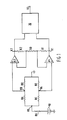
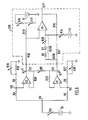
- transducer system circuit diagrams shown in Figures 1, 5, and 6 each present four semiconductor stress sensing elements, i.e. piezoresistors, RA, RB, RC and RD, connected in the same bridge configuration.
- a description of the bridge circuit shown in Figure 1 will suffice to explain the operation of the bridge circuits shown in Figures 5 and 6 also.
- Resistors RA and RB in Figure 1 are connected in series and are tangential and radial piezoresistive sensors, respectively, located in the diaphragm portion of a silicon diaphragm-constraint structure chip with each having an opposite response with respect to the other upon encountering a commonly applied stress to this diaphragm portion as indicated above.
- the interconnection point of resistors RA and RB will have a voltage value designated VB.
- Resistors RC and RD are also located in the diaphragm portion of the chip and connected in series, and are radial and tangential piezoresistive sensors, respectively.
- the interconnection point of resistors RC and RD will have a voltage value designated VA.
- the tangential and radial sensors within both series pairs shown in Figure 1 can, of course, be interchanged in circuit component position in the bridge circuit while remaining in the same geometrical locations in the diaphragm portion. In doing so, the polarity of the bridge output signal would be reversed.
- interconnection of resistors RA and RC is adapted to be connected to a source of excitation voltage, 10, having a value V0.
- Source 10 though shown with a battery symbol, may well be some other common source of constant polarity voltage.
- the interconnection point of resistors RA and RC will have a voltage value designated VX.
- the interconnection point of resistors RB and RD is connected to the circuit zero reference voltage, i.e. ground.
- the bridge output signal voltages in Figure 1 taken between the interconnection point of resistors RA and RB, on the one hand, and the interconnection point of resistors RC and RD on the other, are therefore voltages VA and VB.
- the output signal voltage indication from the bridge circuit chosen for further signal processing because it represents the largest bridge output signal available indicating the stress applied to the chip diaphragm is the difference in value of each of these voltages VA and VB, and so the bridge output signal voltage indicating the applied stress which signal is to be provided to the transducer system signal processing circuitry will be expressed as VB-VA.
- a further bridge output signal voltage indication of some use in the signal processing circuitry, as will be shown later, is expressed VB+VA.
- the sensitivity of the bridge output signal voltage VB-VA to changes in stress applied to the diaphragm portion is, of course, dependent upon the stress sensitivity to such stress changes in the individual sensors or piezoresistors forming the bridge circuit, and also to the value of voltage applied to the bridge, VX, which depends on the value VO of source voltage 10.
- a resistor RX shown as a dashed line component may be provided between source 10 and the interconnection point of resistors RA and RC.
- the voltage applied to the bridge, VX will be dependent upon the value of source voltage 10 and the ratio of resistor RX and the effective impedance of the bridge piezoresistors RA and RB in parallel with piezoresistors RC and RD.
- the resistance value of RX will be taken to be zero in the following until stated otherwise.
- the change in voltage in response to a stress applied to the diaphragm portion of the chip at the circuit point VA will be twice that if only a single sensor was used as previously indicated which could be accomplished in the circuit of Figure 1 by having constructed the chip so that only resistor RA was sensitive to stress while resistors RB, RC, and RD were not.
- the output signal voltages VA and VB are also oppositely acting in response to a stress applied to the chip diaphragm.
- each of the semiconductor piezoresistive sensors, RA, RB, RC and RD have both a temperature coefficient of resistance or TCR, and also a piezoresistive stress sensitivity temperature coefficient or Pi temperature coefficient, with each of these coefficients depending primarily on the maximum dopant concentration occurring in the semiconductor material in the chip diaphragm region forming the piezoresistive sensor.
- the senor When the maximum dopant concentration of the piezoresistive sensor region in the semiconductor material is in the range of 10 17 to 10 20 atom/cm 3 , the sensor exhibits reasonably good stress sensitivity, and further exhibits conveniently useful TCR and Pi characteristics. In this range of dopant concentration, the TCR value changes strongly with changes in the maximum dopant concentration, whereas the Pi characteristic is not significantly affected for the same changes in the maximum dopant concentration. Thus, the TCR of the piezoresistive sensor can be varied by selecting a particular dopant concentration while the Pi characteristic will remain relatively constant in the dopant concentration range indicated.
- the dopant distribution including the maximum dopant concentration within the sensors, may readily be controlled in fabricating each integrated circuit transducer chip so that any multiple sensors therein, i.e. piezoresistors RA, RB, RC, and RD in Figure 1, can be provided having matched and substantially equal TCR and Pi characteristics. Such excellent control of the maximum dopant concentration can be achieved by use of ion implantation methods during fabrication.
- the sensor bridge With the TCR matched to one another for each of RA and RB, and for each of RC and RD, the sensor bridge output voltages VA and VB, and therefore the output expressions VB-VA and VB+VA, will remain nearly temperature independent even though each sensor individually has a TCR.
- the repeatability of the Pi temperature coefficient from, diaphragm to diaphragm, i.e. chip to chip, allows the effects of the Pi temperature coefficient to be compensated by the same circuit compensation schemes for each chip, i.e. transducing system.
- the output voltage signal expression for such a bridge circuit, VB-VA, as a function of stress will have a distinctive stress sensitivity temperature characteristic which will be substantially reproducible and repeatable in each chip having this bridge system made by this process with sensors, or piezoresistors, of this configuration.
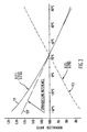
- FIG. 2 Shown in Figure 2 is a typical bridge output signal voltage characteristic, presenting VB-VA versus stress for the four-element piezoresistive sensor bridge system shown in Figure 1.
- Bridge system responses to stress applied to the chip diaphragm each of differing temperatures T0, T1, and T2 are shown. Two effects are observed:
- the temperature related variance in the stress sensor bridge system output voltage signal expression VB-VA is determined with a "zero pressure" input applied externally to the sensor diaphragm.
- the "zero pressure” variance in VB-VA is usually defined as the "null shift", and is just that due to thermally induced stress which was indicated above to be also designated SHIFT.
- Another pressure basis could be used, but note that at any other pressure input, the variance cannot be resolved into that part . caused by differences in the Pi temperature coefficient and that part caused by thermally induced stress.
- included in the measured null Shift are any contributions to the variance in VB-VA caused by mismatch in the TCR's of the bridge sensors, although typically this contribution is very small.
- compensation circuitry must be provided capable of permitting both temperature compensation of the stress sensor sensitivity and also temperature compensation of the stress sensor bridge output voltage null shift. Further, linearity compensation schemes to render the bridge sensor system characteristics more nearly linear with temperature may also be required in some applications depending on the precision required.
- the sensor bridge circuit is connected to a balanced, dual-amplifier stage, as part of the signal processing circuit, which includes two operational amplifiers, A1 and A2, each of which has an input upon which impressing an electrical signal voltage leads to an output signal which is an inverted and scaled version of the signal impressed on that input thereof, and an input associated with a non-inverted, scaled output result.
- Each of amplifiers A1 and A2 has the typical operational amplifier characteristics of high gain, high input impedance, low output impedance, and each has sufficiently small input offset voltages and currents and a sufficiently large output voltage slew rate capability.
- Each of operational amplifiers A1 and A2 makes use of two sources of constant polarity voltage of different voltage values to operate but such sources and the interconnections required are not shown in Figure 1 for amplifiers A1 and A2.
- the interconnection point of piezoresistive sensors RC and RD which presents bridge sensor system output voltage VA, is connected to the noninverting input of amplifier A1.
- the interconnection point of piezoresistor sensors RA and RB which presents bridge sensor system output voltage VB, is connected to the noninverting input of amplifier A2.
- the output of amplifier A1, which provides an output voltage designated V1 is connected back to its inverting input through a resistor, R1; the output of amplifier of A2, which provides an output voltage designated V2, is connected back to its inverting input through another resistor, R2.
- R1 Connected between the inverting inputs of amplifiers A1 and A2 is a further resistor, R0.
- Amplifiers A1 and A2 with resistors R0, R1, and R2 together form a first amplification stage, and this stage provides amplification of the bridge system output voltage signal expression, VB-VA, while passing any common mode voltage appearing at the bridge circuit inputs to A1 and A2 at unity gain.
- the first amplification stage also presents a high input impedance to the voltage signal VB-VA from the bridge system.
- the output signals of the first stage of amplification, output voltages V1 and V2 from amplifiers A1 and A2, respectively, are provided directly to the inputs of a second, or output, amplification stage, 20, which can also be viewed as an output transformation stage for converting the first stage differential signal to a single signal with respect to a reference voltage, here being ground.
- Output amplification stage 20, for the present description is a unity gain amplifier stage which provides an output voltage designated V3.
- Output amplification stage 20 need not be a unity gain amplifier. However, if the dual amplifier stage provides all of the gain and the output stage is a unity gain amplifier, the amplification system as presented in Figure 1 will minimize the possible errors introduced by input offset voltage drift and other such signal processing circuitry errors.
- the output amplification stage 20 amplifies having unity gain in this description the voltage expression V2-V1, which is the amplified version of VB-VA, to provide the output voltage V3.
- V2-V1 which is the amplified version of VB-VA
- An expression for the output voltage V3, the bridge circuit-amplification system output voltage, as a function of the bridge system output voltage signal expression VB-VA can be found from well known analysis techniques to be as follows for the circuit of Figure 1:
- the amplifier system gain G in equation (1) is the gain of the balanced dual-amplifier based first amplification stage, including operational amplifiers A1 and A2, times the gain of the output stage which is just one.
- the sensitivity of the stress transducer system i.e. the change in output voltage V3 for a change in input stress, may be found from the foregoing equation through differentiation thereof as the change in bridge system output voltage signal expression VB-VA for a change in stress times the amplifier system gain as is shown in mathematical form in equation (2) assuming the resistance values of R0, R1, and R2 do not depend on stress: where In equation (2), S(T) is the temperature dependent stress sensitivity of the stress sensor bridge system which is a function of the individual piezoresistive sensor characteristics, and bridge excitation voltage 10 of value V0.
- the bridge system stress sensitivity S(T) is sometimes expressed in terms of SPAN which is the algebraic difference between the resultant voltage VB-VA at some selected stress value in the upper range of stress values and some selected stress value in the lower range of stress value, usually zero.
- S(T) is equivalent to SPAN for bridge circuit characteristics in which VB-VA is a linear function of applied stress; otherwise, SPAN represents some averaging of the slope of the bridge circuit characteristic.
- S(T) and SPAN(T) are equivalent.
- the response of the output voltage V3 to a change in applied stress is also dependent upon temperature.
- Compensation for temperature variations in the stress sensor bridge system sensitivity S(T) caused by the piezoresistive stress sensitivity temperature coefficient may be provided by making the gain, G, temperature sensitive in a sense opposite to that of S(T) such that the response of the output voltage V3 to a change in applied stress becomes independent of temperature.
- the gain G(T) at any temperature multiplied by the bridge system stress sensitivity S(T) must equal a constant, i.e.
- aV3/a(stress) must equal a constant which can be termed the system stress sensitivity as V3 is desired to be a linear function of stress independent of temperature.
- the constant for aV3/a(stress) is chosen typically to be the product of the desired nominal operation stress sensitivity and the gain both at the nominal operating temperature TO which will provide the desired change in value of V3 for a given change in applied stress, i.e. the system stress sensitivity.
- equation (2) is first rewritten to make the temperature dependence with G explicit; the dependence of G on temperature will not lead to any change in form of equation (2) since the differentiation of equation (1) in deriving equation (2) was not made with respect to temperature.
- This equation may then be rewritten as follows: G(TO) and S(TO) are gain and sensitivity, respectively, at a selected nominal temperature T0.
- Equation (4) indicates that for ideal temperature compensation G(T) must be inversely proportional to S(T). Sensor bridge stress sensitivity as a function of temperature S(T) may be found from empirical data.
- gain G(T) is considered to be substantially insensitive to stress for the temperature compensation scheme in the following discussion, although this is not necessarily required, and a stress sensitive gain could be utilized in some situations.
- Gain G(T) as described in equation (4) may be made temperature sensitive by controlling either individually, or in combination, the temperature sensitivities of resistors R1, R2 and R0, that is, the temperature coefficients of resistance or the TCR's of these resistors.
- Gain G can be made to have a positive temperature coefficient by making resistors R1 and R2 more sensitive to temperature in a positive direction than is resistor RO as is made clear by the equation for G below equation (1).
- gain G can be made to have a negative temperature coefficient by making resistors R1 and R2 less sensitive to temperature in the positive direction than resistor R0. If these resistors have negative temperature coefficients instead, the effect on the temperature coefficient of gain G(T) will be reversed.
- resistors R0, R1, and R2 could provide either a positive or negative gain G(T) temperature coefficient.
- Equation (4) shows that the gain temperature characteristic must be substantially the inverse of bridge stress sensitivity temperature characteristic S(T).
- S(T) bridge stress sensitivity temperature characteristic
- resistors R0, R1, and R2 are assumed below to have positive temperature coefficients of resistance.
- resistors R1 and R2 are assumed to be more sensitive to temperature than resistor RO, and have substantially identical temperature coefficients, thus providing G(T) with a positive temperature coefficient as can be seen from the equation for G below equation (1). Taking the immediately preceding assumption further, assume that resistor RO is substantially insensitive to temperature.
- resistors R0, R1 and R2 may be made substantially insensitive to stress, for example, by locating them in a manner as described above with reference to resistors 105 and 106 in Figure 4.
- RO can also be made substantially insensitive to temperature, i.e. have a very low TCR, by having a relatively high dopant level on the order of 10 19 impurity atoms/cm 3 .
- R1 and R2 can be set to each have a higher TCR through using a low dopant level on the order of 10 17 ⁇ 10 19 impurity atoms/cm 3 .
- TCR positive temperature coefficient of resistance
- Q gain G as a function of temperature about the selected temperature TO may be expressed to first order by the use of a truncated Taylor expansion series as is shown in equation (5): where and G(TO) is the amplifier system gain at the selected nominal temperature, and K is the effective temperature coefficient of amplifier system gain G(T) with Q, as indicated, equal to the TCR of resistors R1 and R2.
- RO in equation (5) is considered to be substantially temperature independent.
- the stress sensor bridge sensitivity temperature coefficient is shown in Figure 3 to be negative, i.e. as the temperature decreases, the stress sensitivity increases.
- Span temperature compensation can be provided by making G(T) have a positive temperature coefficient, i.e. as the temperature decreases, gain G(T) decreases.
- G(T) is provided with a positive temperature coefficient as indicated above by making resistors R1 or R2 or both have a positive temperature coefficient (TCR) so that amplifier system gain temperature coefficient K as described in equation (6) is positive.
- Shown in Figure 3 by the curve designated 113 is the approximate normalized electrical gain characteristic G(T)/G(TO) of the amplifier system first stage and the output stage together as shown in Figure 1 which characteristic can be seen to have a positive gain temperature coefficient and to be approximately the inverse of curve 111.
- resistors R1 and R2 of the first amplification stage are fabricated in the constraint portion of the silicon diaphragm-constraint structure chip as part of the monolithic integrated circuit being formed in this chip concurrently in the same fabrication process as are piezoresistive resistors sensors RA, RB, RC and RD, these sensors being fabricated in the diaphragm portion of the chip.
- resistors R1 and R2 may be fabricated in the diaphragm portion of the monolithic integrated circuit chip having the diaphragm-constraint arrangement, the resistors being appropriately oriented with respect to the crystalline structure of the silicon material so as to be substantially insensitive to stress, and these resistors being fabricated by the same fabrication process as are piezoresistors RA, RB, RC and RD as indicated above.
- the silicon diaphragm-constraint structure chip thus provides the semiconductor material base for forming the single monolithic integrated circuit shown in Figure 1.
- the circuit components, both in the diaphragm and in the constraint portions, are formed near or on, or both near and on, a major surface of the silicon chip.
- Resistors R1 and R2 are formed concurrently with, and so have the same impurity dopant distribution as, the piezoresistive stress sensors RA, RB, RC and RD. This manner of fabricating the piezoresistor means they also must have a positive TCR if resistors R1 and R2 are fabricated having a positive TCR as required of them for effecting compensation as indicated above.
- Resistors R1 and R2 may be oriented in any convenient manner with respect to the silicon lattice planes in a manner as described with reference to resistor 105 in Figure 4 if placed in the constraint portion, and so may exhibit piezoresistance, or alternatively may be oriented in a specific manner as described with reference to resistor 106 in Figure 4 if placed in the diaphragm portion.
- the preferred manner of fabricating semiconductor piezoresistive stress sensors RA, RB, RC and RD is through the ion-implantation process. As described earlier, these piezoresistors are provided, at least in part, in the diaphragm portion of the chip supported by a constraint portion in the chip. If a piezoresistor is located in the constraint portion only as opposed to being in any way in the diaphragm portion, such as R1 and R2, such a piezoresistor will be substantially isolated from an applied stress and will not exhibit a significant response to stress applied to the diaphragm portion.
- the TCR is for any of the commonly formed piezoresistors, primarily related to the maximum impurity dopant concentration (impurity atoms/cm 3 ) supplied by the ion-implant impurity dose (ion/cm 2 ).
- impurity atoms/cm 3 the maximum impurity dopant concentration supplied by the ion-implant impurity dose (ion/cm 2 ).
- a temperature sensitive resistor having a selected TCR and being substantially insensitive to stress can be provided in and on the silicon diaphragm-constraint structure chip along with the piezoresistive resistor sensors concurrently in the same fabrication process to form a monolithic integrated circuit in that chip.
- the TCR designated Q of resistors R1 and R2 was assumed to be constant with temperature resulting in G(T) being substantially linear with temperature as can be seen from the equation G below equation (1).
- resistors R1 and R2 are semiconductor resistors as just described, i.e. having an impurity concentration, the TCR is somewhat dependent on temperature resulting in G(T) being somewhat nonlinear. This, of course, may not always be true as advances in technology occur.
- G(T)/G(TO) and S(T1)/S(TO) were determined for different impurity concentrations, each sensor RA, RB, RC and RD and resistors R1 and R2 having substantially an identical dopant distribution. Analysis of these characteristics showed that there existed a range of impurity concentrations which substantially satisfied equation (4), i.e. G(T)/G(T0) being inversely proportional to S(T)/S(TO). As indicated earlier, it was noted that in an impurity concentration range of 10 17 to 10 20 atoms/cm 3 that S(T)/S(TO) remains substantially constant with changes in impurity concentration.
- G(T)/G(TO) in the same impurity concentration range exhibits both a change in the average TCR as well as the temperature characteristic with changes in concentration.
- impurity concentrations which result in bridge stress sensitivity (SPAN) temperature compensation.
- impurity concentration that can be selected to provide piezoresistive stress sensors RA, RB, RC and RD with adequate stress sensitivity, and also provide resistors R1 and R2 as piezoresistors having a TCR temperature characteristic which compensates the piezoresistive sensor bridge stress sensitivity temperature coefficient.
- Resistor RO was also fabricated in the same integrated circuit chip as the stress sensors in the form of a diffused resistor, diffused into the chip semiconductor material concurrently with the diffusion of bases for the bipolar transistors in the amplifiers into the same material, with RO having a substantially lower TCR than the piezoresistors R1 and R2, and having a resistance value in a range of 0.5-1.0 Kohms.
- the transducer output voltage V3 is proportional to the amplifier system gain G which is inversely related to the value of resistance R0.
- resistance RO can be selected to provide the transducer with a selected output voltage V3 sensitivity to stress, aV3/a(stress).
- the TCR of resistance RO in order to provide gain G with a positive temperature coefficient, the TCR of resistance RO must be less than the effective TCR of the sum of resistors R1 or R2.
- resistor RO of Figure 1 there are various other methods of fabricating resistor RO of Figure 1 for the integrated circuit to be formed in connection with the silicon diaphragm-constraint structure chip having sufficiently low TCR characteristics to be less than the effective TCR of the sum of resistors R1 and R2, and which can also be adjusted in resistance value after initial fabrication to thereby adjust gain G.
- One method of fabricating RO in an integrated circuit is the use of chrome-silicon resistors based on thin film technology. Chrome-silicon thin film resistors are capable of having a TCR less than 200 ppm (parts per million), i.e. less than .02%. Such resistors are capable of adjustment by laser trimming, either a manually or a computer controlled laser trimmer.
- Resistor RO could also be provided by a network of parallel branches each containing a base diffused resistor. Adjustment can be provided thereof by either laser or abrasive cutting open selected parallel branches resulting in an increased value of R0. As is common to both of the above methods of providing adjustable resistor R0, the effective resistor can only be increased in resistance value. In some instances, it may be desirable to provide an adjustable resistor which can be incrementally decreased in resistance value.
- One technique of providing a resistance between two points in an integrated circuit that can be decreased from a large resistance value to a smaller one is to provide a number of parallel circuit branches in the semiconductor material connected between each of these points.
- One circuit branch contains a diffused or ion-implanted resistor of a resistance value clearly larger than the resistance value ultimately desired between the two points.
- the remaining circuit branches each comprising a diffused or ion-implanted resistor in series with a pn junction diode, the diodes being reversed biased.
- the resistors in these branches are also of a resistance value larger than the ultimately desired value between the two points.
- a high voltage or a laser beam is applied to selected diodes to electrically short the diodes.
- a resistor is thereby added in parallel between the two points for each diode so rendered a short circuit to cause the effective resistance between the two points to decrease.
- resistors or resistor networks therefor may be located in and on, or just on, the silicon diaphragm-constraint structure chip in and on which the circuit of Figure 1 is fabricated in a manner already described with reference to resistors 105 and 106 in Figure 4.
- chrome silicon thin film resistors will always be substantially insensitive to stress since they do not exhibit any significant stress response characteristics unlike semiconductors which exhibit significant piezoresistive effects as heretofore indicated.
- the stress sensitivity of the stress sensor bridge system of the circuit of Figure 1 as a function of temperature is nonlinear.
- the sensor for the most part has been found to be more sensitive to stress at the colder temperatures than at the warmer temeratures as indicated by the normalized sensitivity curve 111 and the straight line reference 112 in Figure 3.
- the TCR of each of the temperature sensitivity gain resistors R1 and R2 at temperature TO is chosen as that the compensation they provide in the Figure 1 circuit will be the best "average" compensation for the nonlinear bridge circuit stress sensitivity temperature coefficient.
- the linear gain temperature coefficient K in equation (5) for G(T) if made positive, compensates a nonlinear S(T) characteristic according to equation (3) for an S(T) characteristic which increases with decreasing temperature as it does in Figure 3.
- the accuracy desired may require effectively "equalizing" the magnitude of the deviations in the overall stress sensitivity at the desired operating temperature extremes. This could be accomplished by making the gaps between curve 111 and line 112 in Figure 3 at opposite temperature extremes substantially equal to one another.
- the circuit of Figure 1, where resistor RX shown in dashed lines takes on a nonzero resistance value, provides the capability of adjusting rather precisely the temperature compensation of the stress sensor bridge system sensitivity insofar as equalizing the deviation in stress sensitivity at a pair of selected opposite temperature extremes from that sensitivity occurring at temperature TO extrapolated to these extremes.
- the excitation voltage for the stress sensor bridge circuit is supplied by constant polarity voltage source 10 in series with resistor RX.
- Resistor RX is fabricated in a manner similar to resistor RO so as to be substantially insensitive to temperature as compared with resistors R1 and R2 or the piezoresistive resistors in the bridge circuit, to be substantially isolated from stress, and to be capable of adjustment.
- the excitation voltage for the stress sensor bridge is voltage VX which is applied between the two points where the series resistor pair RA and RB, in Figure 1, are interconnected with the series resistor pair RC and RD.
- VX voltage
- RX resistance value
- VX The decrease in VX at temperatures below TO reduces the sensitivity of the sensor bridge system output voltage VB-VA for a change in applied stress since the bridge system output voltage sensitivity to stress is proportional to the applied bridge system voltage, VX.
- the piezoresistive stress sensor resistance value proportionately increases. This results in a lesser voltage across RX at the higher temperature than previously existed at temperature T0, and a corresponding increase in voltage VX.
- the value of resistance RX directly affects the effective sensor bridge system stress sensitivity, that is, the bridge output voltage signal sensitivity to a change in applied stress.
- the bridge output voltage signal sensitivity VB-VA
- the bridge output voltage signal sensitivity decreases with increasing value of resistance RX at temperature T0.
- the bridge output voltage signal sensitivity will increase with increasing temperature, and will decrease with decreasing temperature.
- an increase in value of resistance RX will modify the bridge system stress sensitivity such that the effective stress sensitivity thereof shown by curve 111, in Figure 3, will rotate counterclockwise with increasing values of RX.
- a proper combination of the value of the amplification resistors R1 and R2 and the value of resistance RX will equalize the magnitudes of the stress sensitivity deviations at system operating temperature extremes above and below the normal ambient operating temperature T0.
- the value of resistance RX can be increased to both reduce the sensitivity of the bridge system at temperatures below TO and increase the sensitivity of the bridge system at temperatures above TO to more nearly equalize the deviation in the stress sensitivity to an applied stress occurring at the temperature extremes from the sensitivity occurring at T0.
- resistance RX may be at some initial value, and provide the amplifier system resistors R1 and R2 with a TCR such that the bridge system stress sensitivity temperature coefficient is overcompensated at temperatures above TO and nearly compensated at temperatures below T0.
- the value of resistance RX can be decreased to both increase the sensitivity of the bridge at temperatures below TO and decrease the sensitivity at temperatures above TO to more equalize the deviation in the stress sensitivity to applied stress occurring at the temperature extremes from the sensitivity occurring at T0.
- a proper combination of values for resistor RX and for temperature sensitive resistors R1 and R2 can provide the desired temperature compensation of the stress sensor bridge circuit stress sensitivity temperature characteristic S(T) resulting in appropriate temperature compensation in the stress transducer circuit to provide the desired overall system stress sensitivity.
- resistors RO and RX may be independently adjusted based on empirical data or computer controlled techniques. In practice, it is convenient to keep R1 equal in size to R2.
- the values of RO and RX may be empirically determined or may be selected based on statistical averages, and then adjusted in a manner appropriate to the structure chosen therefor as already indicated.
- null shift is used to mean the change in output voltage as measured from the "null voltage” at zero applied stress due to a change in temperature from the selected reference temperature T0.
- a means for compensating the null shift is shown in Figure 5 and described below.
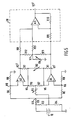
- FIG. 5 Shown in Figure 5 is essentially the transducing apparatus circuit of Figure 1 drawn in a somewhat different form and with the addition of further temperature compensation circuitry to compensate temperature induced "null shift" in the stress sensor bridge output voltage signal.
- the circuit components of Figure 5 which perform the functions of, and are located similarly to, corresponding components in Figure 1 have the same designation symbols in Figure 5 as the corresponding components do in Figure 1.
- a null shift compensation network which includes a first circuit arrangement adjusting operating of the first amplification stage which, as earlier, includes operational amplifiers A1 and A2, and a second circuit arrangement adjusting operation of system output amplification stage 20 which is shown in Figure 5 to include an operational amplifier, A3, this second circuit arrangement being responsive to the output of the first amplification stage.
- These first and second circuit arrangements cooperate with each other to provide temperature compensation of temperature induced null shifts exhibited in the stress sensor bridge system of Figure 1.
- the first circuit arrangement associated with the first amplification stage includes resistors R3, R4, R5, R6 and R7, resistor R5 being capable of adjusted in resistance value.
- Resistors R3, R4, R5, R6 and R7 are substantially insensitive to stress by fabricating them in the same manner already described above with reference to resistors 105 and 106 of Figure 4 in arranging these resistors in and on, or possibly just on, the stress transducer silicon diaphragm-constraint structure chip for the circuit of Figure 5.
- Resistors R5, R6 and R7 are constructed to have a substantially lower TCR than that of resistor R3 by, for example, controlling the dopant concentration thereof, or by fabricating these resistors by use of low TCR thin film methods such as chrome-silicon resistors.
- Adjustable resistor R5 is intended to also have a low TCR relative to that of R3 and may be fabricated in a manner similar to that indicated above for resistor R0.
- R3 is intended to be a temperature sensitive resistor and is constructed in a manner similar to that indicated above for resistors R1 and R2.
- Resistor R5 has a terminating region connected to the common interconnection point of temperature sensitive resistor R3 and resistor R4.
- RX is, of course, optional depending on the desire to affect S(T) at the temperature extremes in use as indicated above, and could be substituted for by a short circuit connection.
- the terminating region of resistor R4 not connected to resistors R3 and R5 is connected to the circuit zero reference voltage, i.e. ground.
- the terminating region of resistor R5 not connected to resistors R3 and R4 is electrically connected to the common interconnection point of resistors R6 and R7.
- the terminating region R7 not connected to resistors R6 and R5 is connected to the common interconnection point of resistors RO and R1 and to the inverting input of amplifier A1.
- the terminating region of resistor R6 not connected to R5 and R7 is connected to the common interconnection point of resistors RO and R2 and to the inverting input of amplifier A2.
- Resistors R3 and R4 form a voltage division network across voltage source 10, source 10 providing a voltage V0, and the R3-R4 divider provides a bias voltage to the inverting inputs of amplifiers A1 and A2 having a value depending on both the resistance value of adjustable resistor R5 and the resistance value of temperature dependent resistor R3 (as well as the R4 value, of course).
- this first circuit arrangement is to cause the output voltage expression V2+V1 of the first amplification stage to be temperature sensitive, the temperature sensitivity thereof primarily dependent upon temperature sensitive resistor R3, but with the differential output voltage of the first amplification stage and with the bridge system output voltage sensitivity to stress being independent of temperature sensitive resistor R3.
- Output amplification stage 20, as shown in Figure 5, includes amplifier A3 which is similar or identical in nature to amplifiers A1 and A2 as indicated above, and a pair of associated closed loop gain setting resistors, R9 and R10.
- Resistor R9 has one terminating region thereof connected to the inverting input of amplifier A3 and the other terminating region thereof connected to the interconnection of resistor R1 and the output of amplifier A1.
- Resistor R10 is connected between the output of amplifier A3 and the inverting input thereof.
- the second circuit arrangement which is essentially a means for setting the transducer system "null voltage" at the output of amplification stage 20.
- the null setting means includes resistors R8, R11, R12, R13 and R14, and which may be considered to be part of an output transformation stage for converting the first stage output differential signal to a single voltage signal with respect to a reference signal, here again ground.
- Resistors R8, R9, R10, R11, R12 and R13 are intended to be substantially insensitive to stress, and may be fabricated in a manner similar to that indicated above for resistors 105 and 106 of Figure 4 in arranging these resistors in and on, or possibly just on, the stress transducer silicon diaphragm-constraint structure chip for the circuit of Figure 5.
- Resistor R14 may be fabricated in the manner indicated above for resistor RO so as to be capable of adjustment and to also be insensitive to temperature and stress.
- resistor R8 has one terminating region thereof connected to the common interconnection point of resistor R13 and the non-inverting input of amplifier A3, and the other terminating region thereof connected to the common interconnection point of resistor R2, resistor R12, and the output of amplifier A2. Also shown, one terminating region of each of resistors R11, R12, R13 and R14, is connected to a common interconnection point. The remaining terminating region of resistor R11 is connected to the common interconnection point of resistors R1 and R9 and the output of amplifier A1. The remaining terminating region of resistor R12 is connected to the common interconnection point of resistors R2 and R8 and the output of amplifier A2. The remaining terminating region of resistor R13 is connected to the common interconnection point of resistor R8 and the non-inverting input of amplifier A3. The remaining terminating region of adjustable resistor R14 is connected to ground.
- the voltages present at the output of amplifiers A1 and A2 from the circuit of Figure 5 are hereafter designated V1' and V2', respectively.
- the null setting input voltage for amplifier A3 is presented at the common interconnection point of resistors R11, R12, R13 and R14, and is designated as voltage V7. From ordinary circuit analysis, the null setting voltage V7 may be mathematically expressed as shown in equation (6).
- equation (6) can be simplified as shown by equation (7).
- the null setting input voltage V7 is directly proportional to the sum of voltages V2' and V1'. Further, the null setting voltage V7 may be adjusted by controlling the value of resistance R14. As also indicated by equation (7), increasing the resistance value of resistor R14 causes the voltage V7 to increase, being limited in maximum value to one-half the sum of the voltages V2' and V1'.
- V2'-V1' represents an amplified version of the bridge system output voltage signal expression VB-VA as it occurs at the output of the first amplification stage.
- the resistance values of resistor R5 and temperature sensitive resistor R3 affect the value of V2'+V1', but without affecting the value of V2'-V1' of the bridge circuit output voltage sensitivity to stress. This allows the output voltage V3' to be temperature compensated for a thermally induced null shift in the sensor bridge without affecting the transducer system sensitivity stress applied to the chip diaphragm.
- the circuit parameters of the first amplification stage including the first circuit means of Figure 5 are arranged to have substantially the following relationships between resistors R1, R2, R6 and R7:
- equations for the output voltage expressions involving V1' and V2' of the amplifier system first stage, including the additional first circuit arrangement can be written as follows from ordinary operational amplifier analysis:
- the first amplification stage output voltage signal expression V2'-V1' represents the voltage signal provided to the input of output amplification stage 20.
- the sensor bridge circuit output voltage signal VB-VA is amplified by gain G' of the first amplification stage.
- Gain G' as shown by equation (11b) is a function of temperature sensitive resistors R1 and R2, and the substantially less temperature sensitive resistors R0, R6 and R7.
- the temperature sensitive gain G' compensates the sensor bridge circuit stress sensitivity temperature coefficient in essentially just the manner that has already been described with reference to the circuit of Figure 1. (Note that equation 11 b is identical to equation (6) in form if RO in equation (6) is replaced by the effective parallel resistance of resistor RO in parallel with the series combination of resistors R6 and R7.)
- the effective temperature coefficient K' of the gain, G' is mathematically shown in equation (13) as it results from using a first order Taylor expansion about TO as before, see equation (5).
- the temperature coefficient K' is directly related to the TCR, Q, of temperature sensitive resistors R1 and R2 in the same general manner as in equation (5).
- resistors R0, R6 and R7 are all taken to be substantially independent of temperature in comparison to R1 and R2.
- the output voltage expression V2+V1 of the first amplification stage is also an input to the output amplification stage 20 and related to determining the null set of that output amplification stage.
- the output expression V2'+V1' of the first amplification stage depends on the first term of equation (12a) which includes as a factor the output expression VB+VA of the sensor bridge circuit; on the second term of equation (12a) which includes as a factor the value VO of supply voltage 10, the value of the second term depending on the resistance value of temperature sensitive resistor R3 and on the resistance value of adjustable resistor R5; and on the third term of equation (12a) which includes as a factor the value of a reference voltage, V', (defined in equation 12b) and on the resistance value of adjustable resistor R5.
- reference voltage V' is dependent upon the voltages V5 and V6. From ordinary operational amplifier analysis, voltage V5 is essentially equal to voltage VA, and voltage V6 is essentially equal to voltage VB. Further, for a balanced bridge, the sum of voltages VA and VB are substantially constant, since as indicated above they vary oppositely in magnitude in response to stress applied to the chip diaphragm, and the sum of voltages V5 and V6 is therefore also substantially constant. Thus, the first term of equation (12a) is essentially constant. The last term of equation (12a) is also essentially constant, at least after resistor R5 is adjusted and then left fixed, since the varying resistance value of resistor R3 in response to changing temperature has a relatively small influence in this third term.
- VA and VB do not depend on the voltage VO of source 10 through resistor R3; hence, since voltages V5 and V6 are essentially equal to voltages VA and VB, voltages V5 and V6 cannot depend to any substantial extent on source 10 and resistor R3 either.
- temperature sensitive resistor R3 decreases with decreasing temperature because of the positive temperature coefficient associated therewith.
- the voltage V2'+V1' decreases as indicated by equation (12a) because that equation shows the second term thereof to be primarily inversely dependent on resistor R3.
- This, in effect, causes the voltage V3' to tend to decrease as indicated in the first term in equation (9).
- the tendency of the transducing system output voltage V3' to increase due to the increase in output voltage signal expression VB-VA caused by the positive null shift with a decrease in temperature, is offset by the tendency of V3' to decrease because of the response of temperature sensitive resistor R3 to the same temperature decrease.
- the amount of compensation provided by the effect of temperature sensitive resistance R3 is determined by adjustable resistor R5.
- equation (12a) if R5 increases to infinity, the latter two terms of equation (12a) are reduced to zero so the resistance value of resistor R5 can significantly control these terms. (Note that the resistance value of R5 going to infinity is equivalent to converting the circuit of Figure 5 to essentially the circuit of Figure 1.)
- the amount of null shift temperature compensation to be provided by the temperature sensitive resistor R3 through the adjustment of resistor R5 can be determined by empirical data. Good results have been obtained by first providing the resistance value of resistor R5 with a very large value to effectively provide negligible null shift temperature compensation. Then, the empirical temperature characteristic data of the transducer can be obtained. Once the data has been obtained, resistance R5 can be decreased in value to provide the desired amount of null shift temperature compensation.
- the transducing system output voltage (the null voltage) for a chosen applied stress may be set as desired at some temperature. This is accomplished, as indicated below equation (7) above, by adjustment of resistance R14.
- temperature sensitive resistors R1, R2 and R3 can be fabricated in the silicon diaphragm-constraint structure chip that piezoresistive sensors RA, RB, RC and RD, are fabricated, and they also will typically be fabricated using common ion implantation process steps. These resistors will have values typically in the order of 5 to 10 Kohms.
- the constant terms K1 and K2 of equations (7) and (8) are dependent upon ratios of the resistance values of resistors R8, R9, R10, R11, R12 and R13, rather than upon absolute resistants values of any of these resistors. Therefore, if these resistors each has a TCR matched to that of every other one, the value of the TCR is relatively unimportant.
- resistors R8, R9, R10, R11, R12 and R13 may also be ion implanted resistors in the chip fabricated during the same process steps, and having the same dopant distribution, as are sensor piezoresistors RA, RB, RC and RD, and gain resistors R1 and R2.
- resistors R9 and R10 will have equal resistance values, approximately 10 Kohms, resulting in output amplification stage 20 having unity gain.
- resistor R11 being approximately equal to resistor R9
- values of resistors R8, R11, R12 and R13 are such that the value of the effective resistance value of resistors R8 and R13 in parallel with R12 (R12 being about 20K) is approximately equal to the value of R11.
- Adjustable resistor R14 will be on the order of 1 to 10 Kohms.
- Resistors R3, R4, R6 and R7 will typically have equal values on the order 5 to 10 Kohms although the value of R3 is, of course, intended to change with temperature while the others are not.
- Adjustable resistor R5 will be on the order of 1 to 40 Kohms.
- each piezoresistive sensor of the bridge circuit arrangement as provided in the diaphragm portion of the silicon diaphragm-constraint structure chip, and the structure of this chip and mount, primarily determine the actual bridge circuit null shift with temperature.
- the bridge circuit characteristic shown in Figure 2 shows a positive shift in the bridge circuit output voltage signal expression VB-VA with a decrease in temperature at a constant applied stress.
- another structure in another chip may lead to the bridge circuit having a negative shift in VB-VA for a decrease in temperature at a constant applied stress.
- R3 as the temperature sensitive resistor in the R3-R4 voltage divider network across source 10, as shown in Figure 5, provides null shift temperature compensation for a sensor bridge system exhibiting the null shift characteristic described in Figure 2, i.e. a positive shift in bridge system output voltage signal expression VB-VA for a decrease in temperature.
- resistor R4 the temperature sensitive resistor in this R3-R4 divider network will provide the necessary null shift temperature compensation for a sensor bridge system exhibiting a negative shift in voltage for a decrease in temperature.
- the selection of which of resistors R3 and R4 is to be made temperature sensitive depends upon the particular null shift characteristics of each piezoresistive sensor bridge circuit structure-chip structure arrangement.
- the resistor RX used for equalizing the deviations in stress sensitivity at the temperature extremes about TO, may be alternatively added to the circuit of Figure 5 in the same manner as shown with reference to Figure 1 with similar results.
- the schematic circuit diagram shown in Figure 6 provides a different circuit arrangement alternate to that shown in Figure 5 for compensating either positive or negative sensor bridge system null shifts.
- the circuit diagram shown in Figure 6 includes a piezoresistive sensor bridge circuit, first amplification stage, and stress sensitivity temperature compensation means similar to that shown in Figure 1. Also shown in Figure 6 are a bi-directional null shift temperature compensation circuit arrangement and an output amplification stage null setting arrangement.
- FIG. 6 Shown in Figure 6 is the piezoresistive sensor bridge circuit including the sensors RA, RB, RC and RD.
- the bridge at the common interconnection point of sensors RA and RC is connected to resistor RX which is in series with constant polarity voltage source 10, this series circuit branch being connected between the bridge circuit and the circuit zero voltage reference, i.e. ground.
- the common interconnection point of resistors RA and RB, and the common interconnection point of resistors RC and RD of the sensor bridge are again connected to the non-inverting inputs of amplifiers Al and A2, respectively, just as. in Figure 1.
- Amplifiers A1 and A2 are of the same nature as similarly designated amplifiers in Figure 1, but here provide output signal voltages designated V1" and V2", respectively.
- resistors R25 and R26, which provide input impedance matching at the inputs of each of amplifiers A1 and A2 to minimize the effects of changing input offset currents in each amplifier due to temperature changes.
- Resistor R25 is connected between the inverting input of amplifier A1 and the common interconnection point of resistors RO and R1.
- Resistor R26 is connected between the inverting input of amplifier A2 and the common interconnection point of resistors RO and R2.
- Resistors R25 is chosen in resistance value such that the current flowing in the inverting input of amplifier A1 is substantially equal to the current flowing in the non-inverting input thereof.
- Resistor R26 is chosen in resistance value so that a similar matched current condition occurs in the two inputs of amplifier A2.
- resistor R25 and R26 Using resistor R25 and R26, the temperature effects of the input offset currents of the amplifiers A1 and A2 are minimized.
- Resistors R25 and R26 being in series with the usually large input impedances of amplifiers A1 and A2, respectively, have negligible other effects on the operation of the circuit of Figure 6. Therefore, no further mention of these resistors will be made in describing the operation of the circuit of Figure 6 below.
- Resistors R25 and R26 are intended to be formed in the same silicon diaphragm-constraint chip. The TCR of these resistors is not critical so that they are formed using any of the fabrication processes already discussed, or other well known processes.
- resistor R1 not connected to resistor RO again is connected to the output of amplifier A1.
- the terminating region of resistor R2 not connected to resistor RO is connected to the output of amplifier A2.
- Resistors R0, R1 and R2 perform the same functions and are constructed in the same manner set out in connection with Figure 1.
- the sensor bridge circuit as shown in Figure 6 has additional circuit components included therein beyond the components included in the bridge circuit shown in Figure 1. These include a parallel combination of resistors, R27 and R28, connected between piezoresistive sensor element RD and ground.
- the bridge circuit further includes a parallel combination of resistors, R29 and R30, connected between piezoresistors sensor element RB and ground.
- Resistors R27 and R29 are intended to be temperature sensitive resistors formed in the same silicon diaphragm-constraint chip as are the piezoresistors RA, RB, RC and RD.
- Resistors R28 and R30 are also to be formed in the same chip and are intended to be resistors subject to being adjusted in resistance value and to be substantially insensitive to temperature relative to resistors R27 or R29, i.e. having a much smaller TCR than do resistors R27 and R29. Further, resistors R27, R28, R29 and R30, are all intended to be substantially insensitive to stress by arranging them in the silicon diaphragm-constraint structure as part of the monolithic integrated circuit corresponding to the Figure 6 diagram being formed in this chip, in a manner similar to resistors 105 and 106 of Figure 4.
- Resistors R27 and R29 may be fabricated in a manner similar to that of resistors R1 and R2, as indicated in connection with Figure 1, such that they may be formed in the same process step that sensor piezoresistors RA, RB, RC and RD, are formed, i.e. all formed in common ion-implantation steps with each having substantially the same dopant distribution.
- resistors R27 and R29 will also have positive temperature coefficients (TCR's) such as are indicated above for each of resistors R1 and R2.
- TCR's positive temperature coefficients
- the temperature sensitivity of resistors R27 and R29 provide temperature compensation for null shift, i.e. the shift with temperature of the bridge circuit output voltage signal expression VB-VA.
- resistors R28 and R30 are intended to be resistor arrangements subject to being adjusted in resistance value.
- Resistors R28 and R30 may be fabricated in a manner similar to resistor RO as set out in connection with describing the circuit of Figure 1.
- the preferable initial values of resistances R28 and R30 in the circuit arrangement of Figure 6 are conveniently values which are less than, or substantially equal to the resistance values of resistors R27 and R29, respectively.
- Resistors R28 and R30 may be adjusted in resistance value in manners as already described for resistor R0.
- resistors R28 and R30 may be chrome silicon thin film resistors fabricated on top of the silicon diaphragm-constraint, monolithic integrated circuit chip. Adjustment of these resistors may be accomplished by laser or abrasive trimming.
- Resistor RX in series with voltage source 10 provides improved sensor circuit performance similar to that as described in connection with Figure 1 by altering the stress sensitivity characteristic of the bridge at temperature extremes above and below T0.
- Resistor RX is, of course, optional as it was in Figure 5, and is intended to be fabricated in and on, or possibly just on, the chip such as to be insensitive to stress, and is also intended to be a resistor having a much lower TCR than the stress sensors.
- RX may be, for example, constructed in a manner similar to RO as set out in connection with describing the circuit of Figure 1.
- Resistors R0, RX, R28 and R30 may all be constructed in the same manner so as to provide the capability of adjustment of the resistance value of each.
- Output amplification stage 200 includes an amplifier, A4, similar or identical in nature to amplifiers A1 and A2, and arranged as a differential operational amplifier simialr to the arrangement of amplifier A3 of Figure 5.
- Output amplification stage 200 further includes a first null setting arrangement connected to the non-inverting input of amplifier A4, a second null setting arrangement connected to the inverting input of amplifier A4, a closed loop gain setting resistor, and an input arrangement for receiving the outputs of the first amplification stage.
- the first null setting arrangement includes the network comprised of a constant polarity voltage source, 11, of the same nature as is source 10 and series pair of connected adjustable resistors, R31 and R32, plus a further resistor, R33.
- Source 11 has one terminal connected to ground, and the other connected to one of the terminating regions of resistor R31.
- the other terminating region of resistor R31 is connected to the common interconnection point of resistors R32 and R33.
- the terminating region of resistor R32 not connected to resistors R31 and R33 is connected to ground.
- Resistor R33 is connected between the common interconnection point of resistors R31 and R32, and the non-inverting input of amplifier A4.
- the second null setting arrangement includes a constant polarity voltage source, 12, of the same nature as is source 10 having one terminal connected to ground. Also included is a resistor, 34, which has one terminating region connected to the other terminal of source 12, and has the other terminating region connected to the inverting input of amplifier A4.
- the closed loop gain of amplifier A4 is substantially determined by resistor R35 which is connected between the output and the inverting input of amplifier A4.
- a first input to output amplification stage 200 taken from the output of amplifier A1 at which is present voltage V1", is provided by a terminating region of a resistor, R37, which is connected to the output of amplifier A1.
- the other terminating region of resistor R37 is connected to the inverting input of amplifier A4.
- a second input to output amplifier stage 200, taken from the output of amplifier A2 at which is present voltage V2" is provided by a terminating region of a resistor, R36, which is connected to the output of amplifier A2.
- the other terminating region of resistor R36 is connected to the non-inverting input of amplifier A4.
- a positive voltage from the voltage divider across source 11 coupled by resistor R33, i.e. from the first null setting arrangement, to the non-inverting input of amplifier A4 will cause the output voltage of the amplifier A4, designated V3", to increase, assuming A4 is not in saturation.
- a positive voltage from source 12 coupled by resistor R34, i.e. from the second null setting arrangement, to the inverting input of amplifier A4 will cause the output voltage V3" to decrease, again assuming A4 is not in saturation.
- the null voltage of the transducer circuit is chosen for a specific temperature and applied stress condition (usually zero applied stress).
- resistor R34 Independent adjustment of resistor R34, or of resistors R31 and R32 together, or of all of these resistors will provide the desired null voltage setting capability for the transducing system through adjusting the output voltage of amplifier A4.
- the second null setting arrangement is simply a Norton equivalent of the first null setting arrangement.
- Many possible arrangements for providing an adjustable voltage bias for use in such null setting are possible, and thus arrangements shown in Figure 6 are only exemplary.
- the portion of the output voltage V3" related to signals in the first amplification stage is equal to the closed loop gain of amplifier A4, as determined by the ratio of resistors R35/R37, multiplied by the differential voltage V2"-V1 ".
- the output "null voltage” portion of V3" is determined by resistance ratio R35/R34, by resistance ratio R31/R32, and by the common voltage value supplied by sources 10, 11 and 12, each having voltage value V0.
- sensor bridge circuits can exhibit either a positive or negative null shift characteristic. That is, at a constant applied stress, the bridge circuit output voltage signal expression VB-VA may increase (positive null shift) or decrease (negative null shift) for an increase in system temperature.
- These potential null shifts when measured at the output of amplifier A4, include all possible temperature induced shifts in the system. They include, for example, both thermally induced stress SHIFT, amplifier input offset voltage and current shifts, and shifts caused by unmatched TCR's in some of the resistor networks.
- the inclusion of the parallel combination of resistors R27 and R28 and the parallel combination of resistors R29 and R30 in the circuit of Figure 6 provides the capability of positive and negative null shift temperature compensation as will be described below.
- these parallel resistor combinations also provide a means for "balancing" the bridge circuit, i.e. setting VA equal to VB at temperature TO with either zero, or some other value, of stress applied to the chip diaphragm.
- bridge balancing is not necessarily reequired.
- the effective resistance value of parallel resistors R27 and R28 may be selected by an appropriate resistance value adjustment of relatively temperature insensitive resistor R28. Increasing the resistance value of R28 causes the voltage VA to increase because of effective voltage divider action of the parallel resistor combination of R27 and R28 in series with sensors RC and RD, and with resistor RX, all in series with source 10. Reducing the resistance value of R28 for the same reason reduces VA. Similarly, the effective resistance value of parallel resistors R29 and R30 may be selected by appropriate adjustment of the relatively temperature insensitive resistor R30.
- Increasing or decreasing R30 causes the voltage VB to correspondingly increase or decrease again because of effective voltage divider action of the parallel combination of resistors R29 and R30 in series with sensors RA and RB, and with RX, all in series with source 10.
- sensor bridge circuit voltage VB can be made equal in value to circuit voltage VA to balance ths sensor bridge circuit.
- the parallel resistor combinations R27-R28, and R29-R30 also provide a means for compensating for either positive or negative sensor bridge circuit null shift.
- Null shift compensation is provided by further adjusting either resistor R28 or R30 to alter the effective TCR of the parallel resistor combinations resulting in a change in the effective TCR of that branch of the sensor bridge circuit containing the parallel resistor combination in which an adjustment occurred to thereby compensate for null shift as will be described in the following.
- parallel resistor combination R27-R28 has an effective resistance designated RPD, and an effective TCR, designated TCR RPO .
- parallel resistor combination R29-R30 has an effective resistance RPB, and an effective TCR, designated TCR RPB .
- the piezoresistor sensors RA, RB, RC and RD, and the temperature sensitive resistors R27 and R29 are assumed to have identical TCR's as will be substantially the situation since they are fabricated concurrently.
- the TCR of adjustable resistors R28 and R30 is substantially lower than the TCR of temperature sensitive resistors R27 and R29, and therefore, adjustable resistors R28 and R30 are assumed, below, to have a zero temperature coefficient.
- the effective TCR of the parallel resistor combinations R27-R28 and R29-R30 may be found by differentiating the effective value of the parallel resistance combinations with respect to temperature, and dividing by the effective resistance at temperature T0.
- An expression for the effective TCR of each of the parallel resistor combinations R27-R28 and R29-R30 are shown in equation (17a) and equation (17b), respectively: where where
- the effective TCR of the parallel resistor combination R27-R28 is, of course, dependent upon the TCR of resistor R27, and the ratio of the resistance values of resistors R27 and R28.
- resistor R28 is adjusted in resistance value from zero to a value much greater than that of resistor R27
- the effective TCR of the parallel resistance combination R27-R28 changes from zero to a value approximately equal to the TCR of resistor R27.
- the resistance value of R30 is adjusted from zero to a value much greater than the value of resistance R29, the TCR of parallel resistor combination R29-R30 changes from zero to a value approximately equal to the TCR of resistor R29.
- the TCR of each of the parallel resistor combinations R27-R28 and R29-R30 may be chosen, within the range possible, by an appropriate choice of resistance values for R28 and R30, respectively.
- Equation (18a) gives an expression for the TCR of the circuit branch containing sensor RD where the parallel resistance combination R27-R28 has an effective resistance value RPD, as indicated above, and a TCR as set out in equation (17a).
- the effective TCR of the circuit branch containing sensor RB is given in equation (18b) below where the parallel resistor combination R29-R30 has an effective resistance value RPB, as indicated above, and a TCR as set out in equation (17b).
- Equations (18a) and (18b) can be further simplified as shown in equations (19a) and (19b) for the situation where the TCR of sensors RB and RD are equal to the TCR of resistors R27 and R29 respectively.
- Equations (19a) and (19b) are similar in nature and therefore only equation (19a) will be discussed.
- the TCR of the circuit branch containing sensor RD is limited to a maximum TCR equal to the TCR of sensor RD. This is so because the factor in equation (19a) multiplying the TCR of sensor RD must always be less than or equal to one since Y1 can never be greater than 1. Note that if the resistance or resistor R28 is zero, the temperature coefficient of the parallel resistor combination R27-R28 is zero because Y1 is zero, and the effective resistance of this parallel combination is also zero. In this situation, equation (19a) shows the effective TCR of the circuit branch containing sensor RD is equal to the TCR of sensor RD.
- adjustable resistors R28 and R30 each are initially set at resistance values which cause the circuit branch containing sensor RD and the circuit branch containing sensor RD, respectively, to each have a minimum TCR. This assures that the branch of the bridge circuit containing sensor RD has an effective TCR less than that of sensor RD alone, and so less than ' that of the circuit branch containing sensor RC which has a TCR equal to that of RD alone as indicated above. Similarly, the branch of the bridge circuit containing sensor RB has an effective TCR less than the branch containing sensor RA.
- the TCR of the circuit branch containing sensor RD was previously at its minimum.
- An increase in the resistance value of adjustable resistor R28 will increase from the minimum the effective TCR of the bridge circuit branch containing sensor RD resulting in voltage VA increasing in resistance value more with temperature because of the increased temperature coefficient of the bridge circuit branch containing resistor RD, than if resistor R28 had not been increased.
- the magnitude of any increase in VB-VA with temperature due to the positive null shift characteristic of the bridge circuit without having changed the resistance value of R28 is reduced by VA increasing faster with temperature after changing the value of R28.
- the positive null shift of the sensor shift system may be more or less compensated by appropriate selection of adjustable resistor R28.
- the increase in resistance value of resistor R28 will compensate for a positive null shift in the transducer system output voltage V3" for positive null shifts from any source in addition to the bridge circuit source.
- the magnitude of the positive null shift is empirically determined at the operating temperature limits of the stress transducer chip.
- the resistance value of R28 is chosen to provide the best overall compensation at both high and low temperature limits noting that the null shift characteristic is not necessarily a linear function of temperature.
- the combination of parallel resistors R27-R28 could be alternately in series with sensor RA, and the combination of parallel resistors R29-R30 could alternately be placed in series with sensor RC. Approximately the same null shift compensation could be achieved for the same changes in the values of resistance of resistors R28 and R30.
- any resistance value adjustment of adjustable resistors R28 and R30 affects not only null compensation but also the bridge balance at zero stress. Any change in bridge balance at zero stress affects the output voltage V3" for zero stress.
- the first and second null setting arrangements are provided for adjustment of V3" after values of R28 and R30 have been selected.
- a practical method of calibrating the circuit of Figure 6 may be accomplished by first balancing the sensor bridge by adjusting the resistance value of either resistor R28 or R30 to cause voltage VB to equal VA. Secondly, the voltages provided by one or both of the first and second null setting arrangements are adjusted by appropriate adjustment of the resistance value of resistors R31, or R32, or R34 to cause voltage V3" to be within the amplifier A4 linear range.
- the transducer system silicon diaphragm-constraint structure chip with an integrated circuit corresponding to the diaphragm at Figure 6 formed in and on this chip, can be tested at operating temperature extremes to determine the actual null shift characteristic and stress sensitivity characteristic of this system so that null compensation may be- provided by appropriate resistance value adjustments of either of resistors R28 or R30.
- RX may then be adjusted in resistance value to appropriately adjust the S(T) characteristic to equalize any deviations at the operating temperature extremes.
- the gain resistor RO may be adjusted to provide the appropriate system sensitivity for the bridge circuit-first amplification stage combination.
- first and second null setting arrangements can then be appropriately adjusted again (adjusting the resistance values of R31, R32 or R34) to provide the desired null voltage of V3" at the output of amplifier A4 for a given stress applied to the chip diaphragm at temperature T0.
- ratios of resistors may be easily controlled, particularly when fabricated by the ion-implantation method.
- the conditions shown in equations (15) and (16) may be easily achieved using this method.
- all resistors shown in Figure 6, with the exception of the adjustable resistors R0, RX, R28, R30, R31, R32 and R34 may be resistors fabricated in common ion-implantation steps.
- R34 may be, for example, base diffused resistors or thin film chrome-silicon resistors which can be provided with very low TCRs.
- Adjustable resistors R0, RX, R28, R30, R31, R32 and R34 may be provided in and on, or possibly just on, the stress transducer integrated circuit chip in a manner of fabrication similar to that earlier described for resistor R0, in connection with Figure 1. Again, these adjustable resistors may be fabricated in and on, or just on, the integrated circuit chip in a manner to permit adjustment by either increasing or decreasing the resistance value thereof.
- the adjustable resistors might be thin or thick film resistors initially set to a value known to be lower than that ultimately desired, and then material in such a resistor may be trimmed away by the laser beam or sandblasting as appropriate until the correct resistance value is reached.
- resistors may be fabricated on top of the diaphragm constraint monolithic integrated circuit, or off the chip on some other substrate. Thick film fabrication thereof may be done on some substrate other than the chip. Alternatively, the resistor-diode circuit arrangement as described with reference to resistor RO might be used to arrive at their desired resistance values. It is important to note that according to equation (16), for the null voltage portion of V3" to be insensitive to temperature, the TCR's of R31 and R32, and the TCR's of R34 and R35 should be substantially equal. Since resistors R31 and R32 are of the same structure, the TCR's thereof will generally be equal.
- R35 from the above discussion is a non-adjustable ion-implant resistor whereas R34 is suggested to be adjustable and so possibly to have a different structure with a different TCR than R35. It is desirable that R34 should be of a selected value rather than being adjustable, and further, should be an ion-implant resistor like resistor R35 so as to have the same TCR. Null setting would then be confined to resistors R31 and R32.
- the stress sensitivity characteristic shown in Figure 2 for a typical sensor bridge system of the kind shown in Figures 1, 5 and 6, can be seen to exhibit a nonlinear stress sensitivity characteristic.
- This nonlinear phenomenon appears to be related to the specific structure design used for the sensors in the bridge system produced in the transducer diaphragm-constraint combination monolithic integrated circuit structure. In some circuit applications, the accuracy requirement will necessitate providing stress sensitivity linearity compensation.
- the linearity compensation network shown in Figure 6 includes an adjustable resistor, R39, and a pair of diodes, D1 and D2.
- the circuit further includes a pair of resistors, R37A and R37B, which are to be considered substitutes for resistor R37.
- a series combination is formed of resistor R39 and diodes D1 and D2 with the cathode of diode D1 connected to the anode of D2, the anode of D1 connected to a terminating region of R39, and the cathode of D2 connected to the common interconnection point of resistors R37A and R37B.
- the remaining terminating region of R39 is connected to the common interconnection point of the inverting input of amplifierA4 and the other terminating region of resistor R37B.
- Resistor R39 is chosen to have a greater resistance value than the value of resistance of resistor R37B.
- the output voltage V3" is proportional to the difference in voltages V2" and V1", multiplied by the effective gain of the output amplification stage which is the resistance value ratio of resistors R35 and R37.
- the output amplification stage effective gain is the resistance ratio value of R35 to the sum of the resistance values, of resistors R37A and R37B.
- One means of modifying the gain at higher stress conditions is to cause the resistance value sum of resistors R37A and R37B to effectively decrease in the output stage gain ratio when differences in voltages V2" and V1" sufficiently increase as the result. of sufficient stress being applied to the chip diaphragm.
- the linearity compensation network shown in Figure 6 provides a circuit for such decreasing of the effective resistance value sum of resistors R37A and R37B.
- the stress sensor bridge circuit begins to respond to this increasing stress and the output voltage V2" will increase and the output voltage V1" will decrease, resulting in the output voltage V3" increasing in a manner described by equation (16).
- the voltage across R37B will be substantially equal to the sum of the forward threshold voltage drops of diodes D1 and D2. Any further increase in stress, i.e. further decrease in V1" and increase in V2", will cause a current to flow through the series combination of resistor R39, and diodes D1 and D2.
- this latter action leads to a current path parallel to that through R37B, thus reducing the effective resistance of R37B and the effective resistance between the output of amplifier A1 and the inverting input of amplifier A4.
- This action results in increasing the gain of the output amplification stage R35/(R37A+R37B) because the effective resistance of the combination of resistor R37B in parallel with the series arrangement of diodes D1 and D2 with resistor R39 is decreasing.
- the amount of stress sensitivity linearity compensation is determined by the resistance of resistor R39 and the forward threshold conduction characteristics of diodes D1 and D2.
- the forward threshold conduction characteristics of diodes D1 and D2 determine the voltage across R37B required before the effective resistance of R37B begins to decrease.
- the amount of linearity compensation is determined by the resistance value of resistor R39.
- resistor-diode networks could be added in parallel with R37B to provide varying amounts of linearity compensation in several different applied stress conditions.
- Other linearity compensation networks similar to the one shown in Figure 6 varying the effective resistor ratio setting the gain of amplifier A4 can provide a change in gain of the output amplification stage as the applied stress to the sensor bridge varies.
- resistor R39 can be a series combination of a fixed resistor and an adjustable resistor.
- the fixed part of resistor R39, and resistors R37A and R37B also, can be fabricated using ion-implantation methods while the adjustable part of R39 can be a low TCR resistor fabricated in the manner described above for fabricating resistor R0.
- diodes D1 and D2 can be provided by pn junction diodes fabricated on the same chip along with all of the circuit components in the circuit arrangement shown in Figure 6.
Landscapes
- Physics & Mathematics (AREA)
- General Physics & Mathematics (AREA)
- Measuring Fluid Pressure (AREA)
- Pressure Sensors (AREA)
- Measurement Of Length, Angles, Or The Like Using Electric Or Magnetic Means (AREA)
Claims (10)
Applications Claiming Priority (2)
| Application Number | Priority Date | Filing Date | Title |
|---|---|---|---|
| US212657 | 1980-12-03 | ||
| US06/212,657 US4345477A (en) | 1980-12-03 | 1980-12-03 | Semiconduction stress sensing apparatus |
Publications (3)
| Publication Number | Publication Date |
|---|---|
| EP0053486A2 EP0053486A2 (de) | 1982-06-09 |
| EP0053486A3 EP0053486A3 (en) | 1984-05-30 |
| EP0053486B1 true EP0053486B1 (de) | 1988-05-11 |
Family
ID=22791941
Family Applications (1)
| Application Number | Title | Priority Date | Filing Date |
|---|---|---|---|
| EP81305595A Expired EP0053486B1 (de) | 1980-12-03 | 1981-11-26 | Spannungsempfindlicher Apparat |
Country Status (5)
| Country | Link |
|---|---|
| US (1) | US4345477A (de) |
| EP (1) | EP0053486B1 (de) |
| JP (1) | JPS57128075A (de) |
| CA (1) | CA1176744A (de) |
| DE (1) | DE3176738D1 (de) |
Families Citing this family (52)
| Publication number | Priority date | Publication date | Assignee | Title |
|---|---|---|---|---|
| US4444056A (en) * | 1982-05-05 | 1984-04-24 | Itt Corporation | Temperature compensated circuit |
| FR2535458B1 (fr) * | 1982-10-29 | 1985-06-14 | Flopetrol Etu Fabrications | Capteur de pression et de temperature |
| JPS59184819A (ja) * | 1983-04-06 | 1984-10-20 | Hitachi Ltd | 半導体圧力センサ |
| JPS59217374A (ja) * | 1983-05-26 | 1984-12-07 | Toyota Central Res & Dev Lab Inc | 半導体ひずみ変換器 |
| JPS60128673A (ja) * | 1983-12-16 | 1985-07-09 | Hitachi Ltd | 半導体感圧装置 |
| JPS6170431A (ja) * | 1984-09-14 | 1986-04-11 | Nippon Cement Co Ltd | 圧力センサ− |
| FR2594546B1 (fr) * | 1986-02-19 | 1988-09-23 | Flopetrol | Dispositif de mesure de la temperature du diaphragme d'un capteur de pression |
| DE3772514D1 (de) * | 1986-10-28 | 1991-10-02 | Sumitomo Electric Industries | Messverfahren fuer einen halbleiter-druckmessfuehler. |
| JPH07113647B2 (ja) * | 1988-09-02 | 1995-12-06 | 日産自動車株式会社 | 半導体加速度センサ |
| US5184520A (en) * | 1989-10-18 | 1993-02-09 | Ishida Scales Mfg. Co., Ltd. | Load sensor |
| US5187985A (en) * | 1991-09-19 | 1993-02-23 | Honeywell Inc. | Amplified pressure transducer |
| JP4236402B2 (ja) * | 2001-10-09 | 2009-03-11 | 富士通マイクロエレクトロニクス株式会社 | 半導体装置 |
| US6870236B2 (en) * | 2003-05-20 | 2005-03-22 | Honeywell International, Inc. | Integrated resistor network for multi-functional use in constant current or constant voltage operation of a pressure sensor |
| US6718830B1 (en) | 2003-05-20 | 2004-04-13 | Honeywell International, Inc. | Customized span compensation of SOI pressure sensor |
| DE10331096B4 (de) * | 2003-07-09 | 2014-02-13 | Austriamicrosystems Ag | Integrierte Halbleiteranordnung und Verfahren |
| US7132838B2 (en) * | 2004-03-11 | 2006-11-07 | Tao Of Systems Integration, Inc. | Active sensor circuit with one or more T-network pairs |
| US7168974B2 (en) * | 2004-04-08 | 2007-01-30 | Leviton Manufacturing Co., Inc. | Three phase lighted plugs and connectors for indicating the absence of at least one phase |
| US7714591B2 (en) * | 2005-12-20 | 2010-05-11 | Kulite Semiconductor Products, Inc. | Apparatus and methods for linearizing piezoresistive wheatstone bridges |
| US8687981B2 (en) | 2007-10-02 | 2014-04-01 | Luxtera, Inc. | Method and system for split voltage domain transmitter circuits |
| US8940598B2 (en) * | 2010-11-03 | 2015-01-27 | Texas Instruments Incorporated | Low temperature coefficient resistor in CMOS flow |
| US9157822B2 (en) * | 2011-02-01 | 2015-10-13 | Kulite Semiconductor Products, Inc. | Electronic interface for LVDT-type pressure transducers using piezoresistive sensors |
| KR101691278B1 (ko) | 2012-05-03 | 2017-01-09 | 애플 인크. | 휨 빔에 의해 지지되는 플랫폼 상의 하중 측정을 위한 모멘트 보상형 휨 빔 센서 |
| JP2014089087A (ja) * | 2012-10-30 | 2014-05-15 | Yamaha Corp | オフセットキャンセル回路 |
| US9983715B2 (en) | 2012-12-17 | 2018-05-29 | Apple Inc. | Force detection in touch devices using piezoelectric sensors |
| US9952703B2 (en) | 2013-03-15 | 2018-04-24 | Apple Inc. | Force sensing of inputs through strain analysis |
| EP2784521B1 (de) | 2013-03-28 | 2019-04-17 | Fraunhofer-Gesellschaft zur Förderung der angewandten Forschung e.V. | Sensoranordnung und Verfahren |
| CN105684177B (zh) | 2013-10-28 | 2019-05-21 | 苹果公司 | 基于压电的力感测 |
| AU2015100011B4 (en) | 2014-01-13 | 2015-07-16 | Apple Inc. | Temperature compensating transparent force sensor |
| US9612170B2 (en) | 2015-07-21 | 2017-04-04 | Apple Inc. | Transparent strain sensors in an electronic device |
| US10055048B2 (en) | 2015-07-31 | 2018-08-21 | Apple Inc. | Noise adaptive force touch |
| US9874965B2 (en) | 2015-09-11 | 2018-01-23 | Apple Inc. | Transparent strain sensors in an electronic device |
| US9886118B2 (en) | 2015-09-30 | 2018-02-06 | Apple Inc. | Transparent force sensitive structures in an electronic device |
| US10006820B2 (en) * | 2016-03-08 | 2018-06-26 | Apple Inc. | Magnetic interference avoidance in resistive sensors |
| US10107873B2 (en) * | 2016-03-10 | 2018-10-23 | Allegro Microsystems, Llc | Electronic circuit for compensating a sensitivity drift of a hall effect element due to stress |
| US10209830B2 (en) | 2016-03-31 | 2019-02-19 | Apple Inc. | Electronic device having direction-dependent strain elements |
| US10365322B2 (en) | 2016-04-19 | 2019-07-30 | Analog Devices Global | Wear-out monitor device |
| US10162017B2 (en) | 2016-07-12 | 2018-12-25 | Allegro Microsystems, Llc | Systems and methods for reducing high order hall plate sensitivity temperature coefficients |
| US10133418B2 (en) | 2016-09-07 | 2018-11-20 | Apple Inc. | Force sensing in an electronic device using a single layer of strain-sensitive structures |
| US10458828B2 (en) * | 2017-02-07 | 2019-10-29 | Honeywell International Inc. | Flow sensor heater circuit calibration |
| US10444091B2 (en) | 2017-04-11 | 2019-10-15 | Apple Inc. | Row column architecture for strain sensing |
| US11024525B2 (en) | 2017-06-12 | 2021-06-01 | Analog Devices International Unlimited Company | Diffusion temperature shock monitor |
| US10309846B2 (en) | 2017-07-24 | 2019-06-04 | Apple Inc. | Magnetic field cancellation for strain sensors |
| US10520559B2 (en) | 2017-08-14 | 2019-12-31 | Allegro Microsystems, Llc | Arrangements for Hall effect elements and vertical epi resistors upon a substrate |
| US20200018662A1 (en) * | 2018-07-11 | 2020-01-16 | King Fahd University Of Petroleum And Minerals | Pipeline leak detection |
| US10782818B2 (en) | 2018-08-29 | 2020-09-22 | Apple Inc. | Load cell array for detection of force input to an electronic device enclosure |
| WO2020046493A1 (en) | 2018-08-29 | 2020-03-05 | Leviton Manufacturing Co., Inc. | Pin and sleeve device with indication |
| WO2020059246A1 (ja) * | 2018-09-21 | 2020-03-26 | パナソニックIpマネジメント株式会社 | センサ処理回路及びセンサシステム |
| CA3125988A1 (en) | 2019-01-07 | 2020-07-16 | Leviton Manufacturing Co., Inc. | An electrical device with built-in sensors and/or communications |
| US11012037B2 (en) | 2019-03-22 | 2021-05-18 | Analog Devices International Unlimited Company | Techniques for controlling an auto-zero amplifier |
| US10833639B2 (en) * | 2019-04-12 | 2020-11-10 | Analog Devices International Unlimited Company | Method for aliasing reduction in auto zero amplifier |
| US20230216449A1 (en) * | 2022-01-03 | 2023-07-06 | Skyworks Solutions, Inc. | Methods for generating a constant current |
| CN115096348B (zh) * | 2022-08-26 | 2022-11-22 | 成都晨电智能科技有限公司 | 一种全桥温漂补偿电路、方法及应变传感系统 |
Citations (2)
| Publication number | Priority date | Publication date | Assignee | Title |
|---|---|---|---|---|
| US4035823A (en) * | 1975-10-06 | 1977-07-12 | Honeywell Inc. | Stress sensor apparatus |
| US4125820A (en) * | 1975-10-06 | 1978-11-14 | Honeywell Inc. | Stress sensor apparatus |
Family Cites Families (15)
| Publication number | Priority date | Publication date | Assignee | Title |
|---|---|---|---|---|
| US3161045A (en) * | 1961-08-18 | 1964-12-15 | Fairchild Camera Instr Co | Strain gauge compensation |
| US3161821A (en) * | 1962-07-02 | 1964-12-15 | Statham Instrument Inc | Wheatstone bridge transducer circuits with external balancing means |
| US3629719A (en) * | 1969-08-22 | 1971-12-21 | Bulova Watch Co Inc | Differential amplifying system |
| US3646815A (en) * | 1970-03-26 | 1972-03-07 | Bailey Meter Co | Silicon pressure transducer circuit |
| GB1414144A (en) * | 1972-03-20 | 1975-11-19 | Welwyn Electric Ltd | Strain measuring device |
| US3893228A (en) * | 1972-10-02 | 1975-07-08 | Motorola Inc | Silicon pressure sensor |
| US3886799A (en) * | 1973-09-24 | 1975-06-03 | Nat Semiconductor Corp | Semiconductor pressure transducer employing temperature compensation circuits and novel heater circuitry |
| US3836796A (en) * | 1973-09-24 | 1974-09-17 | Nat Semiconductor Corp | Semiconductor pressure transducer employing novel temperature compensation means |
| US3841150A (en) * | 1973-11-02 | 1974-10-15 | Honeywell Inc | Strain gauge transducer signal conditioning circuitry |
| US3956927A (en) * | 1975-09-29 | 1976-05-18 | Honeywell Inc. | Strain gauge transducer apparatus |
| JPS52106054U (de) * | 1976-02-09 | 1977-08-12 | ||
| JPS581548B2 (ja) * | 1977-03-17 | 1983-01-11 | 株式会社横河電機製作所 | 薄膜ストレンゲ−ジ変換器 |
| US4202218A (en) * | 1977-09-28 | 1980-05-13 | International Telephone And Telegraph Corporation | Bridge circuit |
| US4205556A (en) * | 1979-02-12 | 1980-06-03 | Rockwell International Corporation | Circuitry for strain sensitive apparatus |
| JPS55113904A (en) * | 1979-02-26 | 1980-09-02 | Hitachi Ltd | Method of zero point temperature compensation for strain-electric signal transducer |
-
1980
- 1980-12-03 US US06/212,657 patent/US4345477A/en not_active Expired - Lifetime
-
1981
- 1981-11-09 CA CA000389753A patent/CA1176744A/en not_active Expired
- 1981-11-26 EP EP81305595A patent/EP0053486B1/de not_active Expired
- 1981-11-26 DE DE8181305595T patent/DE3176738D1/de not_active Expired
- 1981-12-03 JP JP56195087A patent/JPS57128075A/ja active Granted
Patent Citations (2)
| Publication number | Priority date | Publication date | Assignee | Title |
|---|---|---|---|---|
| US4035823A (en) * | 1975-10-06 | 1977-07-12 | Honeywell Inc. | Stress sensor apparatus |
| US4125820A (en) * | 1975-10-06 | 1978-11-14 | Honeywell Inc. | Stress sensor apparatus |
Also Published As
| Publication number | Publication date |
|---|---|
| EP0053486A2 (de) | 1982-06-09 |
| JPH0322065B2 (de) | 1991-03-26 |
| DE3176738D1 (en) | 1988-06-16 |
| JPS57128075A (en) | 1982-08-09 |
| EP0053486A3 (en) | 1984-05-30 |
| CA1176744A (en) | 1984-10-23 |
| US4345477A (en) | 1982-08-24 |
Similar Documents
| Publication | Publication Date | Title |
|---|---|---|
| EP0053486B1 (de) | Spannungsempfindlicher Apparat | |
| US4333349A (en) | Binary balancing apparatus for semiconductor transducer structures | |
| EP0086462B1 (de) | Druckwandler mit Halbleiterdehnungsmessstreifen | |
| US5187985A (en) | Amplified pressure transducer | |
| US4911016A (en) | Semiconductor strain gauge bridge circuit | |
| EP0106050B1 (de) | Druckwandler mit Temperaturausgleichkreis | |
| US6724202B2 (en) | Physical quantity detection device with temperature compensation | |
| US4798093A (en) | Apparatus for sensor compensation | |
| US4465075A (en) | On-chip pressure transducer and temperature compensation circuit therefor | |
| GB2043915A (en) | Semiconductor pressure detector apparatus with zeropoint temperature compensation | |
| EP0034807B1 (de) | Halbleiter-Dehnungsmesser | |
| US4788521A (en) | Temperature compensation system for piezoresistive pressure sensor | |
| US3956927A (en) | Strain gauge transducer apparatus | |
| US4766655A (en) | Method for fabricating a compensated silicon pressure sensing device | |
| US4672853A (en) | Apparatus and method for a pressure-sensitive device | |
| US4442717A (en) | Compensation and normalization apparatus for shear piezoresistive gage sensors | |
| US3922597A (en) | Circuit for detecting a physical quantity | |
| RU2086940C1 (ru) | Полупроводниковый датчик давления | |
| US3753139A (en) | Combined temperature compensation and zero-offset control | |
| JPH0125425B2 (de) | ||
| GB2107876A (en) | Temperature compensation of strain gauges | |
| JP2948958B2 (ja) | トランスジューサ回路 | |
| RU2165602C2 (ru) | Полупроводниковый датчик давления | |
| JPH0634471A (ja) | 半導体圧力センサの出力増幅温度補償回路 | |
| KR100238776B1 (ko) | 압력센서용 온도보상방법 및 그를 이용한 온도보상장치 |
Legal Events
| Date | Code | Title | Description |
|---|---|---|---|
| PUAI | Public reference made under article 153(3) epc to a published international application that has entered the european phase |
Free format text: ORIGINAL CODE: 0009012 |
|
| AK | Designated contracting states |
Designated state(s): DE FR GB IT SE |
|
| PUAL | Search report despatched |
Free format text: ORIGINAL CODE: 0009013 |
|
| AK | Designated contracting states |
Designated state(s): DE FR GB IT SE |
|
| 17P | Request for examination filed |
Effective date: 19850122 |
|
| 17Q | First examination report despatched |
Effective date: 19870721 |
|
| GRAA | (expected) grant |
Free format text: ORIGINAL CODE: 0009210 |
|
| AK | Designated contracting states |
Kind code of ref document: B1 Designated state(s): DE FR GB IT SE |
|
| REF | Corresponds to: |
Ref document number: 3176738 Country of ref document: DE Date of ref document: 19880616 |
|
| ITF | It: translation for a ep patent filed | ||
| ET | Fr: translation filed | ||
| PLBE | No opposition filed within time limit |
Free format text: ORIGINAL CODE: 0009261 |
|
| STAA | Information on the status of an ep patent application or granted ep patent |
Free format text: STATUS: NO OPPOSITION FILED WITHIN TIME LIMIT |
|
| 26N | No opposition filed | ||
| ITTA | It: last paid annual fee | ||
| EAL | Se: european patent in force in sweden |
Ref document number: 81305595.1 |
|
| PGFP | Annual fee paid to national office [announced via postgrant information from national office to epo] |
Ref country code: FR Payment date: 19960918 Year of fee payment: 16 |
|
| PGFP | Annual fee paid to national office [announced via postgrant information from national office to epo] |
Ref country code: DE Payment date: 19960923 Year of fee payment: 16 |
|
| PGFP | Annual fee paid to national office [announced via postgrant information from national office to epo] |
Ref country code: SE Payment date: 19960924 Year of fee payment: 16 Ref country code: GB Payment date: 19960924 Year of fee payment: 16 |
|
| PG25 | Lapsed in a contracting state [announced via postgrant information from national office to epo] |
Ref country code: GB Free format text: LAPSE BECAUSE OF NON-PAYMENT OF DUE FEES Effective date: 19971126 |
|
| PG25 | Lapsed in a contracting state [announced via postgrant information from national office to epo] |
Ref country code: SE Free format text: LAPSE BECAUSE OF NON-PAYMENT OF DUE FEES Effective date: 19971127 |
|
| PG25 | Lapsed in a contracting state [announced via postgrant information from national office to epo] |
Ref country code: FR Free format text: THE PATENT HAS BEEN ANNULLED BY A DECISION OF A NATIONAL AUTHORITY Effective date: 19971130 |
|
| GBPC | Gb: european patent ceased through non-payment of renewal fee |
Effective date: 19971126 |
|
| PG25 | Lapsed in a contracting state [announced via postgrant information from national office to epo] |
Ref country code: DE Free format text: LAPSE BECAUSE OF NON-PAYMENT OF DUE FEES Effective date: 19980801 |
|
| EUG | Se: european patent has lapsed |
Ref document number: 81305595.1 |
|
| REG | Reference to a national code |
Ref country code: FR Ref legal event code: ST |