EP0051133A2 - Photonenemitter und Bildwandler - Google Patents
Photonenemitter und Bildwandler Download PDFInfo
- Publication number
- EP0051133A2 EP0051133A2 EP81107087A EP81107087A EP0051133A2 EP 0051133 A2 EP0051133 A2 EP 0051133A2 EP 81107087 A EP81107087 A EP 81107087A EP 81107087 A EP81107087 A EP 81107087A EP 0051133 A2 EP0051133 A2 EP 0051133A2
- Authority
- EP
- European Patent Office
- Prior art keywords
- region
- photon emitter
- energy
- photon
- junction
- Prior art date
- Legal status (The legal status is an assumption and is not a legal conclusion. Google has not performed a legal analysis and makes no representation as to the accuracy of the status listed.)
- Withdrawn
Links
Images

Classifications
-
- H—ELECTRICITY
- H10—SEMICONDUCTOR DEVICES; ELECTRIC SOLID-STATE DEVICES NOT OTHERWISE PROVIDED FOR
- H10H—INORGANIC LIGHT-EMITTING SEMICONDUCTOR DEVICES HAVING POTENTIAL BARRIERS
- H10H20/00—Individual inorganic light-emitting semiconductor devices having potential barriers, e.g. light-emitting diodes [LED]
- H10H20/80—Constructional details
- H10H20/81—Bodies
- H10H20/811—Bodies having quantum effect structures or superlattices, e.g. tunnel junctions
-
- H—ELECTRICITY
- H10—SEMICONDUCTOR DEVICES; ELECTRIC SOLID-STATE DEVICES NOT OTHERWISE PROVIDED FOR
- H10F—INORGANIC SEMICONDUCTOR DEVICES SENSITIVE TO INFRARED RADIATION, LIGHT, ELECTROMAGNETIC RADIATION OF SHORTER WAVELENGTH OR CORPUSCULAR RADIATION
- H10F55/00—Radiation-sensitive semiconductor devices covered by groups H10F10/00, H10F19/00 or H10F30/00 being structurally associated with electric light sources and electrically or optically coupled thereto
- H10F55/10—Radiation-sensitive semiconductor devices covered by groups H10F10/00, H10F19/00 or H10F30/00 being structurally associated with electric light sources and electrically or optically coupled thereto wherein the radiation-sensitive semiconductor devices control the electric light source, e.g. image converters, image amplifiers or image storage devices
- H10F55/15—Radiation-sensitive semiconductor devices covered by groups H10F10/00, H10F19/00 or H10F30/00 being structurally associated with electric light sources and electrically or optically coupled thereto wherein the radiation-sensitive semiconductor devices control the electric light source, e.g. image converters, image amplifiers or image storage devices wherein the radiation-sensitive devices and the electric light source are all semiconductor devices
- H10F55/155—Radiation-sensitive semiconductor devices covered by groups H10F10/00, H10F19/00 or H10F30/00 being structurally associated with electric light sources and electrically or optically coupled thereto wherein the radiation-sensitive semiconductor devices control the electric light source, e.g. image converters, image amplifiers or image storage devices wherein the radiation-sensitive devices and the electric light source are all semiconductor devices formed in, or on, a common substrate
-
- H—ELECTRICITY
- H10—SEMICONDUCTOR DEVICES; ELECTRIC SOLID-STATE DEVICES NOT OTHERWISE PROVIDED FOR
- H10H—INORGANIC LIGHT-EMITTING SEMICONDUCTOR DEVICES HAVING POTENTIAL BARRIERS
- H10H20/00—Individual inorganic light-emitting semiconductor devices having potential barriers, e.g. light-emitting diodes [LED]
- H10H20/80—Constructional details
- H10H20/81—Bodies
- H10H20/822—Materials of the light-emitting regions
- H10H20/824—Materials of the light-emitting regions comprising only Group III-V materials, e.g. GaP
Definitions
- This invention relates to photon emitters and image converters comprising photon emitters.
- a typical image conversion device emits electrons into a vacuum chamber when relatively low energy photons strike a photo cathode.
- the vacuum chamber has a high externally supplied electric field, requiring about 10,000 volts, which imparts kinetic energy to the electrons and drives them into a phosphor coating at the viewing portion of the device.
- the electrons give up energy to the phosphor causing it to emit a visible radiation. Focusing of the electrons is provided so that an image focused on the cathode is reproduced at a visible wavelength at the phosphor.
- the invention provides a semiconductor photon emitter which finds an application in image converters.
- a photon emitter comprises, according to the invention, a low conductivity semiconductor body having an input region at one end and an output region at the other end, a doped semiconductor region forming a junction with said output region, the doped region being sufficiently thin that the output region is disposed within optical transmission distance of an exposed surface, carrier introduction means to introduce electrical charge carriers into said input region and means to apply an electrical field along the semiconductor body of such a polarity that said electrical charge carriers move from said input region towards said output region, characterised by said output region having a larger energy gap than said input region.
- An image converter comprises, according to the invention, a photon emitter as defined in the preceding paragraph, means to project an image in one waveband onto said input region and means to permit viewing of the image transformed to another waveband at said exposed surface of the body.
- a semiconductor material can be provided with properties such that a low energy carrier present at a lower energy gap region can be moved to a higher energy gap region where a radiative recombination will cause emission of a photon of higher energy.
- the semiconductor material is provided with a region having a smaller bandgap in one portion, an electric field which causes a carrier to drift, in a time which is short compared to the lifetime of the carrier, to a different portion of the semiconductor which is so constructed as to have a set of conditions such that the bandgap will be wider and the electron will recombine radiatively and emit a high energy photon.
- the carrier may be introduced by lower energy photon irradiation or by electrical injection across a junction.
- the invention may be applied to the fabrication of an image converter that is simpler and operates on a lower voltage than any heretofore in the art.
- the invention may also be applied to provide a brighter selectable output frequency solid state light emitter or light emitting diode.
- the low energy carrier can be introduced into the semiconductor either by the irradiating with an external source of low energy photons or in the alternative by an electrical injection of electrons or holes as appropriate in the low bandgap portion of the structure.
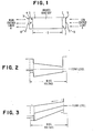
- a semiconductor body 1 is of low extrinsic conductivity or intrinsic semiconductor material and has a graded bandgap which is smaller in the vicinity of a surface 2 and increases to a larger value in the vicinity of a junction 3 with a region of extrinsic conductivity type material 4 that in turn is optically adjacent to a surface 5.
- the distance D between the surface 2 and the junction 3 is governed by the lifetime of the average carrier in the semiconductor material and the magnitude of a bias impressed across the body 1 so that a carrier appearing at 2 can reach the junction 3 during its lifetime. Since a bias is impressed across the body 1, the semiconductor material should be of low extrinsic conductivity or preferably intrinsic to minimize current flow. Further, the lower the extrinsic conductivity, the higher the lifetime and the less stringent the dimension D will be.
- a carrier having a first energy will be moved under the influence of bias to a portion of the body 1 having a higher energy gap where a radiative recombination can take place at the junction 3 emitting a high energy photon shown as light 6 which passes through the relatively thin extrinsic conductivity type region 4 illustrated as P, and emerges through the surface 5.
- the thickness of the region 4 should be such that a radiative recombination occurring at the junction 3 will have the light therefrom minimally attenuated before emerging from the surface 5 as light 6.
- the body 1 is formed such that the portion of the body 1 in the vicinity of the surface 2 is of gallium arsenide and the portion of the body 1 in the region of the junction 3 is of aluminum arsenide with a relatively linear grading of x in the expression Ga x Al 1-x As between, there will be a 1.4 electron volt bandgap at the surface 2 and a 2.16 electron volt bandgap at the junction 3.
- Such a structure will have a direct bandgap for an aluminum content up to about 35%. Beyond this level to the point where it becomes pure aluminum arsenide, the material will have an indirect bandgap.
- the indirect bandgap portion does not have a significant effect since most recombination takes place at the junction 3 and little recombination takes place in the intrinsic portion of the body.
- a region 7 such as AlAs, is provided to prevent surface recombination of the carriers introduced by low energy light 8 focused through the surface 9 to the surface 2.
- the region 7 has a wider bandgap than the body 1 adjacent to the surface 2.
- Ohmic contacts 10 and 11 are provided to apply a bias across the device thereby providing an electric field between the surface 2 and the junction 3.
- the dimension D from the surface 2 to the junction 3 for the material Ga (1-x) Al x As is of the order of 10 micrometers.
- the p region 4 is very thin, about 1 micrometer, is doped to about 10 , and is of aluminum arsenide with a bandgap of about 1.85 electron volts.
- the surface recombination control region 7 of AlAs has a bandgap of 2.16 electron volts, is about 1 micrometer thick and is epitaxial with the GaAs portion of the body 1.
- the GaAs portion of the body 1 at the junction 2 has a bandgap of 1.4 electron volts.
- the device is irradiated from a source of light shown as arrows 8 of low energy photons through the surface 9 and the surface recombination control region 7 to the surface 2.
- FIG. 2 the conditions of the invention are illustrated in terms of an energy level diagram wherein the wide bandgap in region 4 of FIG. 1 abruptly shifts across the junction 3 and then narrows relatively linearly through the body 1 along the distance D to a narrower value adjacent the surface 2 where it abruptly again widens in the surface recombination control region 7.
- FIG. 3 the influence of bias on the energy level diagram is illustrated.
- the effect of the bias is to shift the levels such that for the type of carriers illustrated (electrons) an electron appearing at the surface 2 is caused by the bias to move in the direction of the junction 3 where a radiative recombination with a hole at the junction occurs at a higher bandgap and a higher energy photon is generated.
- the regenerative recycling of photons is enhanced in the device of this invention.
- the regenerative recycling of photon phenomenon is described in the Journal of Applied Physics, 50, (10) October 1979, page 6353.
- photons created by radiative recombination of carriers near a p-n junction are reabsorbed when they travel in a direction of lower bandgap energy material.
- the reabsorbed photons generate new excited carriers which recombine emitting photons of lower energy than the absorbed photons.
- any emitted photon at the junction 3 can emerge from the semiconductor as light 6 through the surface 5.
- the bias voltage should be sufficient to move the electron all the way in the direction of the junction 3 within its lifetime.
- the bias voltage should not be so high that excessive joule heating will result.
- the lifetime of an electron will be about 1x10 -8 seconds and such an electron will drift through the 10 micron distance D in approximately 1x10 -9 seconds requiring a velocity of 1x10 6 centimeters per second. Since the mobility of electrons is about 5000 cm 2 per volt-second, the electric field will be governed by the expression:
- Each component listed in TABLE I can, with appropriate doping be made intrinsic or with either p and n extrinsic type conductivity with two exceptions.
- the exceptions are that the material InSb can only be made intrinsic and the material ZnSe cannot be doped p type.
- FIG. 4 wherein the photon emitter described with reference to FIG. 1 is embodied in a solid state image converter.
- FIG. 4 a transparent substrate 20 is provided which will not seriously attenuate the low energy light which is shown as dotted lines emanating from an object 21.
- the structure of FIG. 1 is positioned on the opposite surface of the substrate 20 from the object 21, the structure of FIG. 1 is positioned.
- the structure is a monocrystalline member 22 having a graded energy gap intrinsic region 23-with the low energy gap portion at a surface 24 which is contiguous with a surface recombination control region 25.
- a fine electrical grid is placed on the surface 26 of the region 25 in contact with the substrate.
- the grid should be either transparent or occupy in the vicinity of 3% of the area and be electrically connected to electrical lead 27.
- a p conductivity type region 28 forms a junction 29 with the high bandgap energy portion of the region 23.
- An electrical grid 30 is applied to the surface 31 and is connected to an electrical lead 32.
- a bias is applied across the region 23 by connecting the leads 27 and 32 to a battery 33.
- the low energy photons from the image 21 pass through the substrate and produce carriers at the low energy portion of the graded bandgap region 23.
- the carriers are moved by the bias field to the junction 29 where they recombine radiatively at a higher energy and an image 34 appears on the surface 31 at a wavelength that is more readily visible than that of the image 21.
- the substrate 2 0 can be Al 2 0 3 about 1 millimeter thick. Vapor deposited aluminum ohmic grid contacts covering about 3% of the area are formed both on the face 31 and on the face 26. All other dimensions are as set forth as for Ga (1-x) Al x As example in connection with FIG. 1.
- the bias from battery 33 is about 0.4 volts.
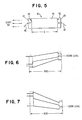
- the principle of the invention may also be applied where the carriers are electrically injected into the field driven graded energy gap material.
- a body 40 having a graded energy gap and high extrinsic or preferably intrinsic conductivity type and consisting of any of the materials of TABLE I except for zinc selenide is provided with a graded energy gap region 41 having a lower energy gap at a junction 42 with an n conductivity type region 43 and a higher energy gap at a junction 44 with a p conductivity type region 45.
- a bias voltage is provided through contacts 46 and 47 which operates to inject carriers at the junction 42 into the lower energy gap portion of the intrinsic region 41 where they drift under the influence of the bias field to recombine at the junction 44.
- the radiative recombination results in higher intensity photons escaping as light shown as arrows 48.
- the energy level conditions are as set forth in the energy diagram of FIG. 6 wherein electrons are injected at the interface corresponding to the junction 42 of FIG. 5.
- the energy level diagram of FIG. 7 is applicable in the case of a material such as zinc selenide, or in a situation where carrier types are reversed.
- FIG. 7. In this case, holes are injected at the junction 42 and are caused to drift where they recombine radiatively with electrons at the junction 44.
- the photons from the radiative recombination are represented by arrows 48 emanating from the p region 44.
- the illumination 48 is brighter due to the enhanced recycling feature which adds the photons which would normally be lost due to absorption by the semiconductor. This may be contrasted with a standard p-intrinsic-n light emitting diode wherein the I region does not have a graded bandgap.
- either the device of FIG. 1 or the device of FIG. 5 can be combined with conventional detectors such as charge-coupled devices or silicon diodes.
- the structure of the invention is a solid state energy converter which takes a low energy carrier and converts it to a photon of a higher energy.
Landscapes
- Photo Coupler, Interrupter, Optical-To-Optical Conversion Devices (AREA)
- Led Devices (AREA)
- Light Receiving Elements (AREA)
- Luminescent Compositions (AREA)
Applications Claiming Priority (2)
| Application Number | Priority Date | Filing Date | Title |
|---|---|---|---|
| US20304080A | 1980-11-03 | 1980-11-03 | |
| US203040 | 1980-11-03 |
Publications (2)
| Publication Number | Publication Date |
|---|---|
| EP0051133A2 true EP0051133A2 (de) | 1982-05-12 |
| EP0051133A3 EP0051133A3 (de) | 1983-03-16 |
Family
ID=22752216
Family Applications (1)
| Application Number | Title | Priority Date | Filing Date |
|---|---|---|---|
| EP81107087A Withdrawn EP0051133A3 (de) | 1980-11-03 | 1981-09-09 | Photonenemitter und Bildwandler |
Country Status (4)
| Country | Link |
|---|---|
| EP (1) | EP0051133A3 (de) |
| JP (1) | JPS6025913B2 (de) |
| AU (1) | AU7671881A (de) |
| BR (1) | BR8106997A (de) |
Cited By (2)
| Publication number | Priority date | Publication date | Assignee | Title |
|---|---|---|---|---|
| FR2733858A1 (fr) * | 1995-05-04 | 1996-11-08 | Ca Nat Research Council | Convertisseur de lumiere d'infrarouge lointain au proche infrarouge |
| WO2010132539A3 (en) * | 2009-05-14 | 2011-05-05 | Photonic Glass Corporation | Methods and apparatus for wavelength conversion in solar cells and solar cell covers |
Family Cites Families (3)
| Publication number | Priority date | Publication date | Assignee | Title |
|---|---|---|---|---|
| US3290568A (en) * | 1963-06-12 | 1966-12-06 | Philco Corp | Solid state, thin film triode with a graded energy band gap |
| GB1450627A (en) * | 1974-01-29 | 1976-09-22 | Standard Telephones Cables Ltd | Opto-electronic devices |
| DE2847451C2 (de) * | 1978-11-02 | 1986-06-12 | Telefunken electronic GmbH, 7100 Heilbronn | Halbleiterbauelement und Verfahren zum Herstellen |
-
1981
- 1981-08-18 JP JP56128309A patent/JPS6025913B2/ja not_active Expired
- 1981-09-09 EP EP81107087A patent/EP0051133A3/de not_active Withdrawn
- 1981-10-22 AU AU76718/81A patent/AU7671881A/en not_active Abandoned
- 1981-10-29 BR BR8106997A patent/BR8106997A/pt unknown
Cited By (2)
| Publication number | Priority date | Publication date | Assignee | Title |
|---|---|---|---|---|
| FR2733858A1 (fr) * | 1995-05-04 | 1996-11-08 | Ca Nat Research Council | Convertisseur de lumiere d'infrarouge lointain au proche infrarouge |
| WO2010132539A3 (en) * | 2009-05-14 | 2011-05-05 | Photonic Glass Corporation | Methods and apparatus for wavelength conversion in solar cells and solar cell covers |
Also Published As
| Publication number | Publication date |
|---|---|
| EP0051133A3 (de) | 1983-03-16 |
| AU7671881A (en) | 1982-05-13 |
| JPS5780782A (en) | 1982-05-20 |
| BR8106997A (pt) | 1982-07-13 |
| JPS6025913B2 (ja) | 1985-06-20 |
Similar Documents
| Publication | Publication Date | Title |
|---|---|---|
| US4202000A (en) | Diode capable of alternately functioning as an emitter and detector of light of the same wavelength | |
| US5525539A (en) | Method for forming a light emitting diode for use as an efficient emitter or detector of light at a common wavelength | |
| US4352117A (en) | Electron source | |
| US4683399A (en) | Silicon vacuum electron devices | |
| US3283160A (en) | Photoelectronic semiconductor devices comprising an injection luminescent diode and a light sensitive diode with a common n-region | |
| CA2000024C (en) | Resonant tunneling semiconductor devices | |
| US4694318A (en) | Sawtooth photodetector | |
| GB2085655A (en) | Semiconductor photodiode | |
| Sasaki et al. | Optoelectronic integrated device with light amplification and optical bistability | |
| US3852797A (en) | Electroluminescent semiconductor device | |
| Pankove et al. | A pnpn optical switch | |
| Sandhu et al. | Near-infrared to visible up-conversion in a forward-biased Schottky diode with ap-doped channel | |
| EP0115591A2 (de) | Photodiode und Photodetektor mit einer Reihe integrierter Photodioden | |
| EP0051133A2 (de) | Photonenemitter und Bildwandler | |
| Donnelly et al. | MIS electroluminescent diodes in ZnTe | |
| Kressel et al. | AN OPTOELECTRONIC COLD CATHODE USING AN AlxGa1− xAs HETEROJUNCTION STRUCTURE | |
| EP0566278B1 (de) | Halbleiterphotokoppler | |
| Shay et al. | CdSnP2 EMISSION AND DETECTION OF NEAR‐INFRARED RADIATION | |
| US4217597A (en) | Diode which transmits and receives light-rays of the same predetermined wavelength and optical telecommunications device using such a diode | |
| GB2253303A (en) | A semiconducter light emitting device | |
| US3745429A (en) | Controllable junction device and radiationgenerating method of utilizing it | |
| US5216538A (en) | Electric-signal amplifying device using light transmission | |
| US3447044A (en) | Scanned line radiation source using a reverse biased p-n junction adjacent a gunn diode | |
| US3636416A (en) | Light-emitting diode with subnanosecond response time | |
| US4620132A (en) | Electron beam scannable LED display device |
Legal Events
| Date | Code | Title | Description |
|---|---|---|---|
| PUAI | Public reference made under article 153(3) epc to a published international application that has entered the european phase |
Free format text: ORIGINAL CODE: 0009012 |
|
| 17P | Request for examination filed |
Effective date: 19810909 |
|
| AK | Designated contracting states |
Designated state(s): BE CH DE FR GB IT NL SE |
|
| PUAL | Search report despatched |
Free format text: ORIGINAL CODE: 0009013 |
|
| AK | Designated contracting states |
Designated state(s): BE CH DE FR GB IT LI NL SE |
|
| STAA | Information on the status of an ep patent application or granted ep patent |
Free format text: STATUS: THE APPLICATION IS DEEMED TO BE WITHDRAWN |
|
| 18D | Application deemed to be withdrawn |
Effective date: 19831222 |
|
| RIN1 | Information on inventor provided before grant (corrected) |
Inventor name: WOODALL, JERRY MCPHERSON Inventor name: LANZA, CONRAD |