EP0051092A1 - Treiberschaltung für eine Kathodenstrahlröhre - Google Patents
Treiberschaltung für eine Kathodenstrahlröhre Download PDFInfo
- Publication number
- EP0051092A1 EP0051092A1 EP80303881A EP80303881A EP0051092A1 EP 0051092 A1 EP0051092 A1 EP 0051092A1 EP 80303881 A EP80303881 A EP 80303881A EP 80303881 A EP80303881 A EP 80303881A EP 0051092 A1 EP0051092 A1 EP 0051092A1
- Authority
- EP
- European Patent Office
- Prior art keywords
- deflection
- drive circuitry
- oscillator
- screen
- line
- Prior art date
- Legal status (The legal status is an assumption and is not a legal conclusion. Google has not performed a legal analysis and makes no representation as to the accuracy of the status listed.)
- Granted
Links
- 230000003466 anti-cipated effect Effects 0.000 claims abstract description 5
- 238000010894 electron beam technology Methods 0.000 claims description 7
- 230000001360 synchronised effect Effects 0.000 claims description 2
- 230000002457 bidirectional effect Effects 0.000 abstract description 12
- 238000012937 correction Methods 0.000 abstract description 7
- 239000003990 capacitor Substances 0.000 description 8
- 241000226585 Antennaria plantaginifolia Species 0.000 description 4
- 230000008901 benefit Effects 0.000 description 3
- 239000004020 conductor Substances 0.000 description 3
- 230000000694 effects Effects 0.000 description 3
- 238000000034 method Methods 0.000 description 3
- 230000004075 alteration Effects 0.000 description 2
- 230000008859 change Effects 0.000 description 2
- 230000010355 oscillation Effects 0.000 description 2
- OAICVXFJPJFONN-UHFFFAOYSA-N Phosphorus Chemical compound [P] OAICVXFJPJFONN-UHFFFAOYSA-N 0.000 description 1
- 238000005282 brightening Methods 0.000 description 1
- 230000003247 decreasing effect Effects 0.000 description 1
- 230000001419 dependent effect Effects 0.000 description 1
- 238000010586 diagram Methods 0.000 description 1
- 238000005516 engineering process Methods 0.000 description 1
- 230000007774 longterm Effects 0.000 description 1
- 230000003252 repetitive effect Effects 0.000 description 1
- 230000004044 response Effects 0.000 description 1
- 230000002441 reversible effect Effects 0.000 description 1
- 239000007787 solid Substances 0.000 description 1
- 238000004804 winding Methods 0.000 description 1
- 229910000859 α-Fe Inorganic materials 0.000 description 1
Images


Classifications
-
- G—PHYSICS
- G09—EDUCATION; CRYPTOGRAPHY; DISPLAY; ADVERTISING; SEALS
- G09G—ARRANGEMENTS OR CIRCUITS FOR CONTROL OF INDICATING DEVICES USING STATIC MEANS TO PRESENT VARIABLE INFORMATION
- G09G1/00—Control arrangements or circuits, of interest only in connection with cathode-ray tube indicators; General aspects or details, e.g. selection emphasis on particular characters, dashed line or dotted line generation; Preprocessing of data
- G09G1/04—Deflection circuits ; Constructional details not otherwise provided for
-
- H—ELECTRICITY
- H04—ELECTRIC COMMUNICATION TECHNIQUE
- H04N—PICTORIAL COMMUNICATION, e.g. TELEVISION
- H04N3/00—Scanning details of television systems; Combination thereof with generation of supply voltages
- H04N3/10—Scanning details of television systems; Combination thereof with generation of supply voltages by means not exclusively optical-mechanical
- H04N3/16—Scanning details of television systems; Combination thereof with generation of supply voltages by means not exclusively optical-mechanical by deflecting electron beam in cathode-ray tube, e.g. scanning corrections
- H04N3/22—Circuits for controlling dimensions, shape or centering of picture on screen
- H04N3/23—Distortion correction, e.g. for pincushion distortion correction, S-correction
- H04N3/233—Distortion correction, e.g. for pincushion distortion correction, S-correction using active elements
- H04N3/2335—Distortion correction, e.g. for pincushion distortion correction, S-correction using active elements with calculating means
Definitions
- This invention relates to drive circuitry for a cathode ray tube.
- the cathode ray tube can display images consisting of over four million picture elements (pels) produced by the momentary brightening of the cathode ray beam as it is caused to scan a raster across the tube screen.
- pels picture elements
- Such a requirement implies a line frequency of about 100 kHz which would impose extremely high stresses on the active device in conventional circuitry which relies on sawtooth wave generators.
- a high line frequency means a short flyback time during which stored energy must be removed from the deflection coils. Because of imperfect switching performance at these power levels the peak collector dissipation in the line scan transistor can reach lKw with an average value of about 50w. Such stresses will lead to component failure and consequent device unreliability. Providing suitable components raises the costs of the drive circuitry to unacceptable values and means that advantage cannot be taken of integrated circuit techniques.
- a bidirectional raster is described, for example, in the IBM Technical Disclosure Bulletin, Volume 21, No 12, May 1979 at pages 5025 and 5026.
- a sinusoidal deflection waveform is described, for example, in the IBM Technical Disclosure Bulletin, Volume 14, No 4, September 1971 at pages 1118 and 1119.
- One problem with such techniques however is how to achieve adequate linearity of the line scan.
- a second problem is present when bidirectional scanning is employed and the ferrite core of the deflection yoke exhibits hysteresis or the drive waveform contains asymmetric distortion components. These aberrations cause vertical misalignment of the pels in alternate scan lines.
- a prime object of the invention is to provide cathode ray tube drive circuitry which employs means for correcting for non-linearity of the line scan, thereby avoiding the image distortions mentioned above.
- the invention is particularly valuable in a bidirectional raster scan arrangement employing a sinusoidal line scan waveform in which the sinusoidal waveform is generated using a tuned circuit of which the deflection yoke forms a part.
- cathode ray tube drive circuitry comprises means for tracing a raster on the screen including a deflection yoke which is arranged to operate in co-operation with deflection signal generator means so as to cause the electron beam repetitively to trace a line across the screen, and means for generating pel clock pulses each defining an interval during which the intensity of the electron beam is modulated in accordance with the required image, and is characterised in that said circuitry comprises a variable frequency oscillator for producing said pel clock pulses, a digital store containing representations indicative of anticipated varations in scanning speed at certain points of the scanned line, and means for varying the frequency of the oscillator in accordance with the stored representations thereby to correct for anticipated speed variations in the scanning speed by slowing or speeding the oscillator.
- the deflection signal generator operates to generate a sinusoidal deflection waveform and includes a tuned circuit comprising the deflection yoke. Additionally the generator preferably operates to trace successive lines in opposite directions across the screen.
- Figure 1 of the drawings shows a typical system for controlling a cathode ray tube to utilise a raster in displaying an image on the screen.
- the cathode ray tube 1 is provided with X and Y deflection coils, shown schematically at 2, supplied with X and Y deflection currents from current generators 3 and 4 respectively.
- the X-deflection current is a repetitive waveform, such as a sawtooth which causes the electron beam to trace a line across the screen at the line repetition frequency.
- the Y deflection current is a more slowly repeating signal which moves the beam slowly down the screen and returns it quickly to the top of the screen.
- the intensity of the electron beam is controlled by the signal applied to a grid 5 of the electron gun (not shown) generating the beam, which signal operates selectively to reduce the intensity of the beam to below the level at which the phosphor of the screen is stimulated to emit light.
- the signal sometimes called a blank-unblank signal, is supplied from the output of a gate circuit, one input of which is connected to an oscillator 7 which supplies a stream of gating pulses which will be called hereinafter the pel clock pulses, the term "pel" meaning picture element i.e., the smallest element of the display image generated at the screen.
- the other input to gate 6 is a video signal at terminal 8. How this signal is generated forms no part of the present invention.
- FIG. 3 shows a simplified standard output circuit for horizontal deflection in which a transistor 9 is used to switch a contant voltage across the deflection coils 10. In combination with the coil inductance this gives a linear rise of current with time and hence a linear angular deflection of the electron beam.
- the switch is turned off and the coil inductance forms a resonant circuit with a parallel capacitor 11.
- the voltage at point X first rises to a large positive value when the current through the coils 10 is zero and then drops to zero when the current has reversed to -I. At this time the switch 9 is turned on again to being the next sweep.
- This circuit has quite low power dissipation since stored energy is neatly transferred from the inductance of the coils 10 to the capacitor 11 and back again. Also the transistor 9 is only conducting when the voltage across it is small. However during the flyback the peak voltage across the transistor is very high and this, combined with fairly large deflection current needed, necessitates an expensive device.
- Figure 4 shows one embodiment of the invention, in which synchronisation of the pel clock with the sinusoidal X-deflection waveform is effected by means of a phase-locked loop.
- the pel clock frequency is varied to compensate for the differences between the real horizontal speed of the electron spot and the desired constant speed.
- the pel clock signals are generated by a voltage controlled oscillator 13 and are provided on conductor 14 for use as described with reference to Figure 1.
- a counter 15 counts up to the number of pel clock pulses required for each pair of forward and backware scan lines. When the number of pulses has been counted the counter 15 emits a pulse on conductor 16.
- Conductor 16 is connected as input to a sample and hold circuit 18 which receives on line 19 the X-deflection waveform from the deflection coils.
- the remainder of the phase-locked loop consists of resistor R1, amplifier 20, low-pass filter 21 and resistor R2.
- Variable resistor R3 is provided to enable adjustment of the position of the picture elements on the raster line, i.e., to move them as a block to the right or left.
- Counter 15 also provides at line 22 signals for selecting the pel to be displayed in each clock period in known fashion.
- a store 23 is provided which contains the speed corrections required to correct image distortion for each sector into which a pair of scan lines has been notionally divided. These are accessed in turn in response to the signals on line 17 and are read to digital-to-analogue converter 24 and integrator 25.
- the output of integrator 25 is connected to a resistor R4 which forms with resistor R2 a summing circuit connected as control input to the voltage controlled oscillator 13.
- the portion of the control input provided via R 4 is arranged to sum to zero over a pair of scan lines.
- the adjustment of oscillator 13 is in the same sense as the relative magnitudes of the real and ideal deflection currents. If the rate of change of the real deflection current is larger than the predetermined value, the beam is moving faster than is appropriate for linearity, causing the pels to be more spaced out than they should be. In this case the frequency of the pel clock should be increased. If the rate of change of the deflection current is less than the ideal, the opposite situation exists and the frequency of the pel clock should be decreased. This is illustrated in Figure 5.
- straight line 26 represents an ideal deflection waveform for linearity.
- the pel oscillator 8 Figure 4 provides pulses at times tl, t2 and t3.
- the deflection waveform is imperfect, as represented by curve 27, pulses at times tl, t2 and t3 will cause the pels to be located incorrectly at points dl', d2' and d3' along the scan line.
- the pels will be in their correct positions dl, d2 and d3.
- the deflection coils can be made part of a resonant circuit. If this is parallel tuned then the bulk of the deflection current circulates within the circuit and the active devices need only replenish circuit losses. A tap on the tuned circuit can be used to reduce the driving impedance to a reasonable value.
- Figure 6 shows such a parallel tuned arrangement.
- Drive circuit 28 having a high output impedance provides reasonable voltage and current (for example 10 volts and 1 amp) and with the value of capacitor C2 very much larger than capacitor C1 a high voltage of approximately 1000 volts, 2 amps can be provided in the deflection coil 10.
- FIG. 7 A practical circuit is shown in Figure 7 in which a 50 kHz sinusoidal waveform of 1.2 volts peak is applied to an input 29 connected to the positive input of amplifier 30.
- the amplifier 30 shown is an SGS-ATES audio amplifier type T D A 2010.
- the numbers around the periphery of the amplifier represent the pin numbers of the amplifier.
- the solid plates of the electrolytic capacitors of 100 pf, 25 volts working voltage, represent the negative plates of these capacitors.
- this circuit will produce a sinusoidal voltage in the deflection coil 10 (shown as having an inductance of 3.1 mH) of 1350 volts, 1.4 amps peak.
- a fundamental advantage of a sinusoidal system is that component stresses are essentially independent of frequency. With the sawtooth circuit of Figure 3, higher frequency means a shorter flyback time and a higher peak voltage.
- Each pair of scan lines is divided into a number of zones, the store 23 supplying a parameter to vary the speed of the VCO 13.
- the values of the parameter for each zone can be chosen to make the pel spacing and position on the screen exactly as desired.
- the digital store 23 may either be a read only store programmed at the factory or a random access memory whose contents are set up as a result of some user adjustment procedure.
- the vertical deflection must be performed by a staircase waveform rather than the usual ramp to avoid line pairing at the sides of the screen. This could be provided by a line counter feeding a D/A converter.
- the video data stream must be supplied in reverse order on alternate lines. It is envisaged that high- content displays will normally use a bit-per-pel buffer for refresh. In this case the words of the buffer can easily be addressed in descending order on alternate lines and a bidirectional shift register can be used for the final serialisation.
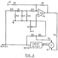
- Figure 8 is a schematic of the complete sinusoidal deflection generator and showing how E-W pincushion correction can be applied to the circuit of Figure 7 using an analogue multiplier 31, for example a Motorola Type MC1494 multiplier, connected to the input 29, Figure 7.
- the two inputs 32 and 33 to the multiplier 31 are from the voltage divider constituted by resistors R5 and R6 and from operational amplifier 34.
- the multiplier 31 functions as an amplifier with the voltage divider constituted by resistors R5 and R6 reducing the voltage appearing across the yoke 10, Figure 7 and supplying the reduced voltage on input line 32.
- the gain is determined by a control voltage on line 33 from operational amplifier 34.
- the signal path from line 32 to line 29 completes a positive feedback loop through the amplifier 30, Figure 7 to form a sinewave oscillator circuit.
- the amplitude of oscillation, and hence the picture width, is stabilized by detecting the peak amplitude of the deflection coil voltage, comparing it with a target value and adjusting the control voltage on line 33 accordingly.
- the target value is a function, for example parabolic, of the vertical beam position to effect E-W (east-west) pincushion correction.
- the pincushion correction waveform is applied to input 35.
- Variable resistor R7 allows the width of the picture to be controlled.
- Resistors R8 and R11 perform a summing function at the negative input of the operational amplifier 34.
- Resistor R8 provides an input indicative of the vertical position of the electron spot and resistor R11 provides an input dependent on the amplitude of the horizontal deflection.
- the amplifier 34 compares the sum of these two components with a constant voltage adjusted by variable resistor R7 and any difference is amplified with a gain determined by resistor R9 which provides negative feedback. The amplified difference is used as a control input to the multiplier 31 to vary the loop gain of the horizontal oscillator 30, Figure 7.
- Diode D1, capacitor Cl, and resistor R12 form a peak detector with input from a potential divider, constituted by resistors R10 and R13 which are connected across the horizontal deflection yoke 10, Figure 7.
- a potential divider constituted by resistors R10 and R13 which are connected across the horizontal deflection yoke 10, Figure 7.
Priority Applications (4)
| Application Number | Priority Date | Filing Date | Title |
|---|---|---|---|
| DE8080303881T DE3068551D1 (en) | 1980-10-31 | 1980-10-31 | Cathode ray tube drive circuitry |
| EP80303881A EP0051092B1 (de) | 1980-10-31 | 1980-10-31 | Treiberschaltung für eine Kathodenstrahlröhre |
| US06/288,862 US4463288A (en) | 1980-10-31 | 1981-07-31 | Cathode ray tube drive circuitry |
| JP56128261A JPS5781290A (en) | 1980-10-31 | 1981-08-18 | Cathode ray tube drive circuit |
Applications Claiming Priority (1)
| Application Number | Priority Date | Filing Date | Title |
|---|---|---|---|
| EP80303881A EP0051092B1 (de) | 1980-10-31 | 1980-10-31 | Treiberschaltung für eine Kathodenstrahlröhre |
Publications (2)
| Publication Number | Publication Date |
|---|---|
| EP0051092A1 true EP0051092A1 (de) | 1982-05-12 |
| EP0051092B1 EP0051092B1 (de) | 1984-07-11 |
Family
ID=8187286
Family Applications (1)
| Application Number | Title | Priority Date | Filing Date |
|---|---|---|---|
| EP80303881A Expired EP0051092B1 (de) | 1980-10-31 | 1980-10-31 | Treiberschaltung für eine Kathodenstrahlröhre |
Country Status (4)
| Country | Link |
|---|---|
| US (1) | US4463288A (de) |
| EP (1) | EP0051092B1 (de) |
| JP (1) | JPS5781290A (de) |
| DE (1) | DE3068551D1 (de) |
Cited By (6)
| Publication number | Priority date | Publication date | Assignee | Title |
|---|---|---|---|---|
| EP0108541A2 (de) * | 1982-11-03 | 1984-05-16 | THORN EMI Ferguson Limited | Fernsehempfänger |
| FR2543776A1 (fr) * | 1983-03-31 | 1984-10-05 | Rca Corp | Agencement de correction de distorsion de la trame dans un systeme de traitement video numerique |
| FR2562360A1 (fr) * | 1984-03-29 | 1985-10-04 | Rca Corp | Circuit de deviation a courant sinusoidal pour le balayage bidirectionnel d'un tube a rayons cathodiques |
| EP0175409A1 (de) * | 1984-09-03 | 1986-03-26 | Koninklijke Philips Electronics N.V. | Bildaufzeichnungs- beziehungsweise Bildwiedergabegerät mit Zeilenablenkschaltung |
| GB2192520A (en) * | 1986-07-03 | 1988-01-13 | Rca Corp | Raster distortion correction circuit |
| EP0589512A2 (de) * | 1992-09-22 | 1994-03-30 | Koninklijke Philips Electronics N.V. | Schaltungsanordnung zur Korrektur der Bildverzerrung in einem Anzeigegerät |
Families Citing this family (10)
| Publication number | Priority date | Publication date | Assignee | Title |
|---|---|---|---|---|
| US4757239A (en) * | 1985-10-18 | 1988-07-12 | Hilliard-Lyons Patent Management, Inc. | CRT display system with automatic alignment employing personality memory |
| US5041764A (en) * | 1990-10-22 | 1991-08-20 | Zenith Electronics Corporation | Horizontal misconvergence correction system for color video display |
| US5168199A (en) * | 1991-08-14 | 1992-12-01 | Loral Corporation | Horizontal linearity correction circuitry for cathode ray tube display |
| US5204589A (en) * | 1992-03-02 | 1993-04-20 | Thomson Consumer Electronics, S.A. | Data signal controlled oscillator for a video display |
| DE69320129T2 (de) * | 1992-09-22 | 1999-03-11 | Philips Electronics Nv | Schaltungsanordnung zur Korrektur der Bildverzerrung in einem Anzeigegerät |
| DE19521816C1 (de) * | 1995-06-16 | 1996-07-04 | Grundig Emv | Bildschirmgerät mit gleichmäßiger Leuchtdichte- und Schärfeverteilung |
| FR2783995B1 (fr) * | 1998-09-30 | 2000-12-08 | St Microelectronics Sa | Circuit de balayage d'un tube cathodique a correction de geometrie independante de la frequence de balayage |
| US6351086B1 (en) * | 1999-09-30 | 2002-02-26 | Thomson Lincensing S. A. | Display correction waveform generator for multiple scanning |
| JP2002010098A (ja) * | 2000-06-27 | 2002-01-11 | Matsushita Electric Ind Co Ltd | 水平偏向回路および双方向水平偏向装置 |
| WO2010008855A1 (en) | 2008-06-23 | 2010-01-21 | Milwaukee Electric Tool Corporation | Electrical component including a battery charger assembly |
Citations (3)
| Publication number | Priority date | Publication date | Assignee | Title |
|---|---|---|---|---|
| US3740608A (en) * | 1970-08-18 | 1973-06-19 | Alphanumeric Inc | Scanning correction methods and systems utilizing stored digital correction values |
| US3809947A (en) * | 1971-12-17 | 1974-05-07 | Ibm | Sine wave deflection system for correcting pincushion distortion |
| US4099092A (en) * | 1976-08-18 | 1978-07-04 | Atari, Inc. | Television display alignment system and method |
Family Cites Families (2)
| Publication number | Priority date | Publication date | Assignee | Title |
|---|---|---|---|---|
| JPS5222214B2 (de) * | 1972-07-01 | 1977-06-16 | ||
| JPS5578690A (en) * | 1978-12-08 | 1980-06-13 | Sony Corp | Horizontal linearity corrector for beam index type color television picture receiver |
-
1980
- 1980-10-31 DE DE8080303881T patent/DE3068551D1/de not_active Expired
- 1980-10-31 EP EP80303881A patent/EP0051092B1/de not_active Expired
-
1981
- 1981-07-31 US US06/288,862 patent/US4463288A/en not_active Expired - Fee Related
- 1981-08-18 JP JP56128261A patent/JPS5781290A/ja active Granted
Patent Citations (3)
| Publication number | Priority date | Publication date | Assignee | Title |
|---|---|---|---|---|
| US3740608A (en) * | 1970-08-18 | 1973-06-19 | Alphanumeric Inc | Scanning correction methods and systems utilizing stored digital correction values |
| US3809947A (en) * | 1971-12-17 | 1974-05-07 | Ibm | Sine wave deflection system for correcting pincushion distortion |
| US4099092A (en) * | 1976-08-18 | 1978-07-04 | Atari, Inc. | Television display alignment system and method |
Cited By (12)
| Publication number | Priority date | Publication date | Assignee | Title |
|---|---|---|---|---|
| EP0108541A2 (de) * | 1982-11-03 | 1984-05-16 | THORN EMI Ferguson Limited | Fernsehempfänger |
| EP0108541A3 (de) * | 1982-11-03 | 1985-09-18 | THORN EMI Ferguson Limited | Fernsehempfänger |
| FR2543776A1 (fr) * | 1983-03-31 | 1984-10-05 | Rca Corp | Agencement de correction de distorsion de la trame dans un systeme de traitement video numerique |
| US4600945A (en) * | 1983-03-31 | 1986-07-15 | Rca Corporation | Digital video processing system with raster distortion correction |
| FR2562360A1 (fr) * | 1984-03-29 | 1985-10-04 | Rca Corp | Circuit de deviation a courant sinusoidal pour le balayage bidirectionnel d'un tube a rayons cathodiques |
| DE3511318A1 (de) * | 1984-03-29 | 1985-10-10 | Rca Corp., Princeton, N.J. | Schaltungsanordnung zur erzeugung eines sinusfoermigen ablenkstroms fuer eine kathodenstrahlroehre |
| US4634940A (en) * | 1984-03-29 | 1987-01-06 | Rca Corporation | Sine wave deflection circuit for bidirectional scanning of a cathode ray tube |
| EP0175409A1 (de) * | 1984-09-03 | 1986-03-26 | Koninklijke Philips Electronics N.V. | Bildaufzeichnungs- beziehungsweise Bildwiedergabegerät mit Zeilenablenkschaltung |
| GB2192520A (en) * | 1986-07-03 | 1988-01-13 | Rca Corp | Raster distortion correction circuit |
| GB2192520B (en) * | 1986-07-03 | 1991-02-13 | Rca Corp | Raster distortion correction circuit |
| EP0589512A2 (de) * | 1992-09-22 | 1994-03-30 | Koninklijke Philips Electronics N.V. | Schaltungsanordnung zur Korrektur der Bildverzerrung in einem Anzeigegerät |
| EP0589512A3 (en) * | 1992-09-22 | 1994-07-13 | Koninkl Philips Electronics Nv | Image distortion correction circuit for use in a display device |
Also Published As
| Publication number | Publication date |
|---|---|
| EP0051092B1 (de) | 1984-07-11 |
| US4463288A (en) | 1984-07-31 |
| JPS5781290A (en) | 1982-05-21 |
| DE3068551D1 (en) | 1984-08-16 |
| JPS6227710B2 (de) | 1987-06-16 |
Similar Documents
| Publication | Publication Date | Title |
|---|---|---|
| EP0051092B1 (de) | Treiberschaltung für eine Kathodenstrahlröhre | |
| US3577031A (en) | Multicolor oscilloscope | |
| US5469029A (en) | Deflection apparatus for raster scanned CRT displays | |
| US5663615A (en) | Reciprocal deflection type CRT displaying apparatus | |
| US4516058A (en) | Linearity corrected horizontal deflection circuit | |
| US4305023A (en) | Raster distortion corrected deflection circuit | |
| US4281340A (en) | Horizontal scanning rate correction apparatus for beam index color cathode-ray tube | |
| FI105631B (fi) | Tyynyvääristymän korjauspiiri käsittäen lokinsiipivääristymän kompensoinnin | |
| US4423358A (en) | Horizontal deflection circuit with linearity correction | |
| US3748531A (en) | Circuit arrangement for generating in a picture display device a sawtooth current of line frequency having an amplitude varying at field frequency | |
| EP0183514B1 (de) | Dynamische Fokussierschaltung | |
| JPH0250476B2 (de) | ||
| US4649325A (en) | Scanning CRT control system | |
| US5466993A (en) | Deflection apparatus for raster scanned CRT displays | |
| US4584503A (en) | Phase correction arrangement for deflection circuit | |
| EP0664644B1 (de) | Ablenkschaltung mit Korrektur von Rasterverzerrungen im inneren Teil des Bildes | |
| US5389859A (en) | Display device including a correction circuit for correcting a position error, and correction circuit for use in such a display device | |
| KR20010013971A (ko) | 수평편향회로 | |
| US4777412A (en) | Gullwing distortion correction circuit | |
| US3946274A (en) | Side pincushion correction circuit | |
| EP0284348B1 (de) | Schaltung zur Korrektur der Möwenflügelverzerrung | |
| EP0589512A2 (de) | Schaltungsanordnung zur Korrektur der Bildverzerrung in einem Anzeigegerät | |
| EP0797350A1 (de) | Horizontalablenkschaltung mit Parallelogramm-Rasterkorrektur | |
| JPH08172543A (ja) | 往復偏向式crtディスプレイ装置 | |
| GB2098424A (en) | Horizontal driver and linearity circuit |
Legal Events
| Date | Code | Title | Description |
|---|---|---|---|
| PUAI | Public reference made under article 153(3) epc to a published international application that has entered the european phase |
Free format text: ORIGINAL CODE: 0009012 |
|
| AK | Designated contracting states |
Designated state(s): DE FR GB |
|
| 17P | Request for examination filed |
Effective date: 19820623 |
|
| GRAA | (expected) grant |
Free format text: ORIGINAL CODE: 0009210 |
|
| AK | Designated contracting states |
Designated state(s): DE FR GB |
|
| REF | Corresponds to: |
Ref document number: 3068551 Country of ref document: DE Date of ref document: 19840816 |
|
| ET | Fr: translation filed | ||
| PLBE | No opposition filed within time limit |
Free format text: ORIGINAL CODE: 0009261 |
|
| STAA | Information on the status of an ep patent application or granted ep patent |
Free format text: STATUS: NO OPPOSITION FILED WITHIN TIME LIMIT |
|
| 26N | No opposition filed | ||
| PGFP | Annual fee paid to national office [announced via postgrant information from national office to epo] |
Ref country code: GB Payment date: 19900911 Year of fee payment: 11 |
|
| PGFP | Annual fee paid to national office [announced via postgrant information from national office to epo] |
Ref country code: FR Payment date: 19900926 Year of fee payment: 11 |
|
| PGFP | Annual fee paid to national office [announced via postgrant information from national office to epo] |
Ref country code: DE Payment date: 19901027 Year of fee payment: 11 |
|
| PG25 | Lapsed in a contracting state [announced via postgrant information from national office to epo] |
Ref country code: GB Effective date: 19911031 |
|
| PG25 | Lapsed in a contracting state [announced via postgrant information from national office to epo] |
Ref country code: FR Effective date: 19920630 |
|
| GBPC | Gb: european patent ceased through non-payment of renewal fee | ||
| PG25 | Lapsed in a contracting state [announced via postgrant information from national office to epo] |
Ref country code: DE Effective date: 19920701 |
|
| REG | Reference to a national code |
Ref country code: FR Ref legal event code: ST |