EP0051028A2 - Münzannahme- oder -rückgabevorrichtung - Google Patents
Münzannahme- oder -rückgabevorrichtung Download PDFInfo
- Publication number
- EP0051028A2 EP0051028A2 EP81401667A EP81401667A EP0051028A2 EP 0051028 A2 EP0051028 A2 EP 0051028A2 EP 81401667 A EP81401667 A EP 81401667A EP 81401667 A EP81401667 A EP 81401667A EP 0051028 A2 EP0051028 A2 EP 0051028A2
- Authority
- EP
- European Patent Office
- Prior art keywords
- coin
- cmos
- gate
- output
- oscillator
- Prior art date
- Legal status (The legal status is an assumption and is not a legal conclusion. Google has not performed a legal analysis and makes no representation as to the accuracy of the status listed.)
- Granted
Links
Images
Classifications
-
- G—PHYSICS
- G07—CHECKING-DEVICES
- G07D—HANDLING OF COINS OR VALUABLE PAPERS, e.g. TESTING, SORTING BY DENOMINATIONS, COUNTING, DISPENSING, CHANGING OR DEPOSITING
- G07D5/00—Testing specially adapted to determine the identity or genuineness of coins, e.g. for segregating coins which are unacceptable or alien to a currency
- G07D5/08—Testing the magnetic or electric properties
-
- G—PHYSICS
- G07—CHECKING-DEVICES
- G07D—HANDLING OF COINS OR VALUABLE PAPERS, e.g. TESTING, SORTING BY DENOMINATIONS, COUNTING, DISPENSING, CHANGING OR DEPOSITING
- G07D5/00—Testing specially adapted to determine the identity or genuineness of coins, e.g. for segregating coins which are unacceptable or alien to a currency
Definitions
- the present invention relates to an apparatus for accepting or rejecting a single type of coin, which is designed and constructed only to accept genuine coins of a particular value or denomination, and to reject spurious coins or slugs which may have the same dimensions.
- the present invention also provides an auxiliary coin acceptor-rejector component or device which may readily be fitted into already existing coin operated devices so as to discriminate more accurately between genuine coins and spurious coins or slugs.
- the present invention provides an improvement in a single coin acceptor or rejector for use with coin-operated machines constructed in accordance with the disclosure of ourcopending application Serial No.81401630.9 . filed OCTOBER 16, 1981.
- the single coin acceptor or rejector has an oscillator circuit and a sensing coil, wherein the oscillator oscillates at a constant amplitude, and has sufficient gain that it will continue to oscillate at such constant amplitude when a coin is placed within the sensing coil.
- the presence of a coin within the sensing coil gives rise to: (a) a substantial decrease in the Q of the sensing coil; (b) energy losses caused by eddy currents being dissipated by the coin, and energy losses required to overcome the magnetic hysteresis of the coin; and (c) a rise in frequency of the oscillator because the coin acts as a shorted turn of the coil and effectively reduces its inductance.
- the oscillator is designed with enough extra gain to overcome these losses by drawing more current from the supply and thereby to maintain the same amplitude of oscillation.
- a field effect transistor utilized in the circuit becomes in effect a variable resistor, the value of which is controllable by materials passing through the sensing coil, the effective resistance changes being detected by a resistor connected in series with the field effect transistor and which functions as a current to voltage converter.
- Two pairs of comparators, an opto isolator and a triac are relied upon to activate an accept armature of an accept solenoid to accept genuine coins, - all other non-genuine coins being rejected.
- the first parameter provides discrimination by means of the current being proportional to voltage drop.
- the second parameter provided by the present invention is frequency shift caused when a coin passes through the sensing coil.
- FIGS. 1 to 4, inclusive the coin acceptor or rejector therein illustrated corresponds exactly with the coin acceptor or rejector unit illustrated in FIGS. 1 to 4, inclusive, of ourcopending application Serial No. 81401630.9, filed October 16 , 1981.
- Serial No.81401630.9/ reference numerals of each such new component are prefaced with the letter "N".
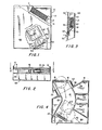
- FIGS. 1 to 4, inclusive omnibus views of the coin acceptor or rejector of the present invention.
- a coin acceptor or rejector unit 10 has an intermediate member 11 having longitudinally- flanged sides 12 which are adapted to receive between them a back member or plate 15.
- the back plate 15 and the intermediate member 11, preferably made of a molded plastic material, at their upper ends together provide a coin receiving slot 16.
- the slot 16, in turn, connects with a coin chute 18, as best seen in FIG. 4, which is of arcuate form so as to direct the coin to an acceptance slot 20, if such coin is shown to be genuine by the unit of the present invention.
- Both the intermediate member 11 and the back plate 15 adjacent the coin receiving slot 16 have matching cutouts 35, 36 around which a tank coil L2 is wound so that a coin inserted in slot 16 will pass through such coil.
- Coil L2 is a sensing coiL as more particularly hereinafter described.
- an accept solenoid L3 which consists essentially of a coil 50, a metallic flapper 51 having inturned flange 52 which projects through mating slot 54 in the intermediate member 11 and the back plate 15 at the base of the chute 18 to block the same and to prevent the passage of a coin for acceptance by the machine to which the unit is applied, if such coin is determined by the unit to be non-genuine.
- the unit In addition to the intermediate molded plastic member 11 and backing plate 15 the unit also has an outer plate 59 which contains on its face all of the solid state components shown in the circuit diagram, which are suitably wired on the back of such plate in accordance with such circuitry. The entire circuit components on the front of such plate 59 are enclosed by a cover 60.
- the metallic flapper 51 is hingedly connected to such plate 59 as at 64 and has a flat body member 65 generally of the size and shape to conform to the size and shape of the solenoid coil 50. It also has a narrowed neck 66 which connects with the outer flanged portion 67 of the flapper.
- a leaf spring 70 is secured to the inner face of the inverted U-shaped member 61 and bears against the top surface of the outer flanged portion 67 of the flapper to hold it in blocking engagement with the mating slot 54 at the lower end of chute 18.
- the electromagnetic force of such solenoid will bring the flapper 51 into contact with the lower face of said solenoid and lift the flange 52 out of the mating slot 54 whereby the coin acceptance chute will be unblocked and the coin will enter the machine to which the unit is applied in the direction shown by arrow 80.
- the coin inserted in slot 16 should be non-genuine or a slug, flange 52 of the flapper will block acceptance of the coin and such coin will be directed to. the rejection chute 84 in the direction shown by the dotted arrow 85.
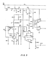
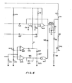
- FIGS. 5 and 6 For a better understanding of the circuitry of the present invention reference will now be made to the accompanying circuit diagram as shown in FIGS. 5 and 6, which should be read together, as one-half of the circuit is shown on FIG. 5 and the other half is shown on F I G. 6.
- each new component is prefaced by the letter "N".
- a source of alternating current is shown, as 50 volts which has a continuous lead 101 to the accept solenoid L3.
- the source also has a branch 102 comprising a resistor 103 which, in turn, supplies an alternating current of 6 volts to resistor R l, diode D l and capacitor Cl, which together comprise a conventional half wave rectifier enabling the unit to be powered by 6 volts AC or DC.
- the resulting DC voltage appearing across capacitor Cl is connected by a limiting resistor R2 and a 6 volt zener diode ZD1 which serves to clamp the output of capacitor Cl at a constant 6 volts.
- Capacitor C2 which is of low value such as one microfarad, is connected between branch 102 and ground and serves to decouple any R.F. noise.
- a positive voltage is applied to the drain of the field effect transistor F.E.T.1 by resistor R3, RF choke Ll and sensing coil L2.
- Capacitors C 6, C7 and C4 provide the necessary phase shift and feedback, respectively, to sustain oscillation.
- the source of the field effect transistor is returned to ground via diode D2 which is provided to compensate for the temperature characteristics of the field effect transistor F.E.T.l.
- resistor R3 is connected in series with the field effect transistor F.E.T.1 so that there is a voltage drop across it, such voltage drop being directly proportional to the current which flows through the field effect transistor.
- Capacitor C3 is connected across resistor R3 to decouple any RF noise at this point.
- Capacitor C8 serves to isolate the quiescent voltage appearing across resistor R3 and pass only changes in voltage to the comparator gates Ml and M2.
- a resistor divided network comprising resistors R 6, R7 and R8 provides a fixed reference voltage to one input of the comparator gates MI and M2, while the resistor divided network comprising variable resistance VRl and resistor R5, provides an adjustable threshold voltage to the other input of the same comparator gates.
- resistor NRl is added in series with variable resistor VRl of the divider network to provide a finer adjustment of the variable resistor VRl.
- comparator gates Ml and M2 It is characteristic of the comparator gates Ml and M2 that whenever the plus input of the gate is more positive than the minus input the output will be high. Conversely, whenever the minus input is more positive than the plus input then the output will be low.
- the reference and threshold voltages are arranged in such a manner that, under no signal conditions the output of comparator M1 will be normally high while the output of comparator M2 will be normally low.
- CMOS NOR gates NQ1 and NQ2 are connected together to form a one-shot multivibrator circuit which functions as follows:
- the time constant of capacitor NC2 and variable resistor NVR1 is selected to be at least two complete cycles of the sensing oscillator waveform. During the "on" period any further positive excursions of the sensing oscillator waveform will not affect the output condition of the CMOS NOR gate NQ2, because the one-shot multivibrator circuit can only be affected by the sensing oscillator when it is in its "off” condition. Any rise in frequency of the sensing oscillator will produce a corresponding increase of constant width pulses at the output of CMOS NOR gate NQ2. It will be understood therefore that as a feature of this invention the duty cycle is a direct function of frequency shift.
- Resistor NR3 and capacitor NC3 form an integrator circuit and the DC voltage developed across capacitor NC3 is directly proportional to the instantaneous duty cycle of the waveform produced by the one-shot multivibrator circuit.
- a typical oscillator frequency of 600 Kcs. a U.S. quarter passing through the sensing coil L2 will raise the oscillator frequency momentarily to 604.2 Kcs.
- the resulting duty cycle changes of the waveform at the output of CMOS NOR gate NQ2 will produce a corresponding voltage rise across capacitor NC3 of approximately 90 millivolts.
- the signal appearing across capacitor NC3 is coupled via capacitor NC4 to the appropriate inputs of a pair of comparator gates NM3 and NM4. These two gates are supplied with a voltage reference through the resistor divider network resistor N R 8, variable resistor NVR2 and resistor NR5.
- the reference voltage at the minus input of comparator NM3 is adjustable by variable resistor NVR2 to a high enough level that only signal amplitudes produced the frequency shift produced by genuine coins will cause it to go “high”.
- the small reference level set by resistor NR5 to the positive input of comparator NM4 is low enough to allow very small signal amplitudes to change its output state from "high” to "low".
- Comparator NM4, CMOS NOR gate NQ3 and their associated components resistor NR6, diode ND4 and capacitor NC5 form what is best described as a second coin detector which is an important feature of the present invention.
- the present invention includes comparative NM4 and CMOS NOR gate NQ3 to discriminate against such spurious coins.
- the function and operation of these two components for this purpose is summarized as follows:
- the opto isolator Oil is connected to the outputs of CMOS NOR gates NQ4 and NQ3 in such a way that the opto isolator Oil is only activated when there is a a coincidence of the two parameters, i.e., amperage and voltage drop on the one hand, and frequency shift on the other hand.
- the photo cell section of opto isolator Oil is connected to form a voltage divider with accept solenoid L3, resistor R13 and resistor R14, and is so designed as to provide sufficient gate current to trigger the triac TR1 whenever the opto isolator Oil is activated.
- the main terminals of the triac TR1 are connected in series with the high voltage AC supply and the accept solenoid coil L3 through leads 101, 104 and 105, thereby activating the accept armature of accept solenoid L3 whenever the opto isolator OIl is activated.
Landscapes
- Physics & Mathematics (AREA)
- General Physics & Mathematics (AREA)
- Testing Of Coins (AREA)
- Control Of Vending Devices And Auxiliary Devices For Vending Devices (AREA)
Applications Claiming Priority (2)
| Application Number | Priority Date | Filing Date | Title |
|---|---|---|---|
| US06/201,583 US4359148A (en) | 1980-10-28 | 1980-10-28 | Coin acceptor or rejector |
| US201583 | 1994-02-25 |
Publications (3)
| Publication Number | Publication Date |
|---|---|
| EP0051028A2 true EP0051028A2 (de) | 1982-05-05 |
| EP0051028A3 EP0051028A3 (en) | 1982-06-23 |
| EP0051028B1 EP0051028B1 (de) | 1987-10-07 |
Family
ID=22746423
Family Applications (1)
| Application Number | Title | Priority Date | Filing Date |
|---|---|---|---|
| EP81401667A Expired EP0051028B1 (de) | 1980-10-28 | 1981-10-22 | Münzannahme- oder -rückgabevorrichtung |
Country Status (10)
| Country | Link |
|---|---|
| US (1) | US4359148A (de) |
| EP (1) | EP0051028B1 (de) |
| JP (1) | JPS57105098A (de) |
| KR (1) | KR860000358B1 (de) |
| AU (1) | AU551829B2 (de) |
| CA (1) | CA1167139A (de) |
| DE (1) | DE3176478D1 (de) |
| ES (1) | ES8206885A1 (de) |
| IL (1) | IL64065A (de) |
| MX (1) | MX151384A (de) |
Cited By (2)
| Publication number | Priority date | Publication date | Assignee | Title |
|---|---|---|---|---|
| GB2151062A (en) * | 1983-11-04 | 1985-07-10 | Mars Inc | Coin validator |
| GB2254948A (en) * | 1991-04-15 | 1992-10-21 | Mars Inc | Coin validation. |
Families Citing this family (10)
| Publication number | Priority date | Publication date | Assignee | Title |
|---|---|---|---|---|
| US4493411A (en) * | 1982-09-29 | 1985-01-15 | Mars, Inc. | Self tuning low frequency phase shift coin examination method and apparatus |
| US4678994A (en) * | 1984-06-27 | 1987-07-07 | Digital Products Corporation | Methods and apparatus employing apparent resonant properties of thin conducting materials |
| JPS62164190A (ja) * | 1986-01-16 | 1987-07-20 | 三洋電機株式会社 | 硬貨識別装置 |
| US4936435A (en) * | 1988-10-11 | 1990-06-26 | Unidynamics Corporation | Coin validating apparatus and method |
| US5067604A (en) * | 1988-11-14 | 1991-11-26 | Bally Manufacturing Corporation | Self teaching coin discriminator |
| US4936436A (en) * | 1989-04-03 | 1990-06-26 | Keltner James P | Push coin acceptor |
| US5028870A (en) * | 1989-04-18 | 1991-07-02 | Environmental Products Corporation | Sensor system method and apparatus for discrimination of metallic objects based on a variation in self inductance |
| JPH0823898B2 (ja) * | 1991-02-28 | 1996-03-06 | 株式会社高見沢サイバネティックス | 金属体弁別装置 |
| JP2766572B2 (ja) * | 1991-12-17 | 1998-06-18 | アルゼ株式会社 | コインセレクタの不正検出装置 |
| WO1998005008A1 (en) | 1996-07-29 | 1998-02-05 | Quadrum Telecommunications, Inc. | Coin validation apparatus |
Family Cites Families (19)
| Publication number | Priority date | Publication date | Assignee | Title |
|---|---|---|---|---|
| US2642974A (en) * | 1949-11-30 | 1953-06-23 | Harold H Ogle Jr | Coin material testing device |
| US3317016A (en) * | 1965-05-21 | 1967-05-02 | Int Nickel Co | Coin selecting device |
| US3453532A (en) * | 1967-09-06 | 1969-07-01 | Robert F Gardiner | Metal detector including a hartley oscillator with field effect transistor and delayed automatic amplitude stabilizing feedback |
| CH459629A (de) * | 1968-02-05 | 1968-07-15 | Autelca Ag | Münzprüfer |
| CA951403A (en) * | 1970-02-16 | 1974-07-16 | Modern Research Inc. | Electric coin detecting apparatus |
| GB1381278A (en) | 1971-11-10 | 1975-01-22 | Eastmead Eng Co Ltd | Apparatus for monitoring coins |
| FR2212589B1 (de) * | 1972-12-29 | 1976-10-29 | Satmam | |
| GB1461404A (en) * | 1973-05-18 | 1977-01-13 | Mars Inc | Coin selection method and apparatus |
| US3901368A (en) * | 1974-03-11 | 1975-08-26 | Lance T Klinger | Coin acceptor/rejector |
| US3956692A (en) * | 1974-12-23 | 1976-05-11 | Wein Products, Inc. | Metal object comparator utilizing a ramp having a V-shaped slot for mounting the object accurately within the test coil |
| US4105105A (en) * | 1975-10-17 | 1978-08-08 | Libandor Trading Corporation Inc. | Method for checking coins and coin checking apparatus for the performance of the aforesaid method |
| US4108296A (en) * | 1976-04-08 | 1978-08-22 | Nippon Coinco Co., Ltd. | Coin receiving apparatus for a vending machine |
| US4184366A (en) * | 1976-06-08 | 1980-01-22 | Butler Frederick R | Coin testing apparatus |
| JPS542196A (en) * | 1977-06-07 | 1979-01-09 | Fuji Electric Co Ltd | Coin screening device |
| US4151904A (en) * | 1977-11-14 | 1979-05-01 | H. R. Electronics Company | Coin detection device |
| US4226323A (en) * | 1978-09-08 | 1980-10-07 | Dautremont Joseph L | Precision coin analyzer for numismatic application |
| US4254857A (en) * | 1978-09-15 | 1981-03-10 | H. R. Electronics Company | Detection device |
| US4257512A (en) * | 1979-02-12 | 1981-03-24 | Bally Manufacturing Corporation | Coin acceptor apparatus |
| US4334604A (en) * | 1979-03-15 | 1982-06-15 | Casino Investment Limited | Coin detecting apparatus for distinguishing genuine coins from slugs, spurious coins and the like |
-
1980
- 1980-10-28 US US06/201,583 patent/US4359148A/en not_active Expired - Lifetime
-
1981
- 1981-10-08 CA CA000387613A patent/CA1167139A/en not_active Expired
- 1981-10-13 AU AU76296/81A patent/AU551829B2/en not_active Ceased
- 1981-10-16 IL IL64065A patent/IL64065A/xx unknown
- 1981-10-22 DE DE8181401667T patent/DE3176478D1/de not_active Expired
- 1981-10-22 EP EP81401667A patent/EP0051028B1/de not_active Expired
- 1981-10-26 ES ES506549A patent/ES8206885A1/es not_active Expired
- 1981-10-27 KR KR1019810004100A patent/KR860000358B1/ko not_active Expired
- 1981-10-28 JP JP56173660A patent/JPS57105098A/ja active Pending
- 1981-10-28 MX MX189867A patent/MX151384A/es unknown
Cited By (4)
| Publication number | Priority date | Publication date | Assignee | Title |
|---|---|---|---|---|
| GB2151062A (en) * | 1983-11-04 | 1985-07-10 | Mars Inc | Coin validator |
| GB2254948A (en) * | 1991-04-15 | 1992-10-21 | Mars Inc | Coin validation. |
| US5213190A (en) * | 1991-04-15 | 1993-05-25 | Mars Incorporate | Method and apparatus for testing coins |
| GB2254948B (en) * | 1991-04-15 | 1995-03-08 | Mars Inc | Apparatus and method for testing coins |
Also Published As
| Publication number | Publication date |
|---|---|
| MX151384A (es) | 1984-11-13 |
| IL64065A (en) | 1987-12-20 |
| AU551829B2 (en) | 1986-05-15 |
| IL64065A0 (en) | 1982-01-31 |
| EP0051028A3 (en) | 1982-06-23 |
| JPS57105098A (en) | 1982-06-30 |
| DE3176478D1 (en) | 1987-11-12 |
| KR830008255A (ko) | 1983-11-16 |
| US4359148A (en) | 1982-11-16 |
| AU7629681A (en) | 1982-05-06 |
| EP0051028B1 (de) | 1987-10-07 |
| CA1167139A (en) | 1984-05-08 |
| ES506549A0 (es) | 1982-09-01 |
| KR860000358B1 (ko) | 1986-04-12 |
| ES8206885A1 (es) | 1982-09-01 |
Similar Documents
| Publication | Publication Date | Title |
|---|---|---|
| EP0051028A2 (de) | Münzannahme- oder -rückgabevorrichtung | |
| US4334604A (en) | Coin detecting apparatus for distinguishing genuine coins from slugs, spurious coins and the like | |
| US4286704A (en) | Coin-validating arrangement | |
| US3918563A (en) | Coin arrival sensor | |
| US3901368A (en) | Coin acceptor/rejector | |
| CA2302922C (en) | Dual coil coin identifier | |
| US4254857A (en) | Detection device | |
| US4469213A (en) | Coin detector system | |
| US4257512A (en) | Coin acceptor apparatus | |
| EP0086226B1 (de) | Vorrichtung zum aufspüren von münzen | |
| JPH03282695A (ja) | 硬貨評価とトークン読取装置 | |
| DE69425758T2 (de) | Münzprüfer mit offset-null-spulen | |
| US5007520A (en) | Microprocessor-controlled apparatus adaptable to environmental changes | |
| EP0664914B1 (de) | Münzprüfer | |
| EP0051017B1 (de) | Münzannahme- oder -rückgabevorrichtung | |
| EP0203702B1 (de) | Bestimmen des Wertes einer sich bewegenden Münze | |
| US4398626A (en) | Low frequency phase shift coin examination method and apparatus | |
| EP0110510A2 (de) | Selbstabstimmende niederfrequente phasenverschiebende Münzprüfmethode und -vorrichtung | |
| CA2184147C (en) | Coin detection device and associated method | |
| EP0282481A1 (de) | Münzengültigkeits-prüfvorrichtung. | |
| US4846332A (en) | Counterfeit coin detector circuit | |
| GB1559577A (en) | Method of checking coins and coin checking apparatus for the aforesaid method | |
| KR910007767B1 (ko) | 경화 판별장치 및 방법 | |
| JPS5838446Y2 (ja) | 貨幣選別装置 | |
| JP3014416U (ja) | ゲーム機用のコイン及びその識別装置 |
Legal Events
| Date | Code | Title | Description |
|---|---|---|---|
| PUAI | Public reference made under article 153(3) epc to a published international application that has entered the european phase |
Free format text: ORIGINAL CODE: 0009012 |
|
| PUAL | Search report despatched |
Free format text: ORIGINAL CODE: 0009013 |
|
| AK | Designated contracting states |
Designated state(s): BE CH DE FR GB IT LU NL |
|
| AK | Designated contracting states |
Designated state(s): BE CH DE FR GB IT LU NL |
|
| 17P | Request for examination filed |
Effective date: 19821217 |
|
| RAP1 | Party data changed (applicant data changed or rights of an application transferred) |
Owner name: THIRD WAVE ELECTRONICS COMPANY, INC. |
|
| GRAA | (expected) grant |
Free format text: ORIGINAL CODE: 0009210 |
|
| RAP1 | Party data changed (applicant data changed or rights of an application transferred) |
Owner name: THIRD WAVE ELECTRONICS COMPANY, INC. |
|
| AK | Designated contracting states |
Kind code of ref document: B1 Designated state(s): BE CH DE FR GB IT LI LU NL |
|
| PG25 | Lapsed in a contracting state [announced via postgrant information from national office to epo] |
Ref country code: NL Effective date: 19871007 Ref country code: IT Free format text: LAPSE BECAUSE OF FAILURE TO SUBMIT A TRANSLATION OF THE DESCRIPTION OR TO PAY THE FEE WITHIN THE PRESCRIBED TIME-LIMIT;WARNING: LAPSES OF ITALIAN PATENTS WITH EFFECTIVE DATE BEFORE 2007 MAY HAVE OCCURRED AT ANY TIME BEFORE 2007. THE CORRECT EFFECTIVE DATE MAY BE DIFFERENT FROM THE ONE RECORDED. Effective date: 19871007 Ref country code: BE Effective date: 19871007 |
|
| PG25 | Lapsed in a contracting state [announced via postgrant information from national office to epo] |
Ref country code: LU Free format text: LAPSE BECAUSE OF NON-PAYMENT OF DUE FEES Effective date: 19871031 Ref country code: LI Effective date: 19871031 Ref country code: CH Effective date: 19871031 |
|
| REF | Corresponds to: |
Ref document number: 3176478 Country of ref document: DE Date of ref document: 19871112 |
|
| ET | Fr: translation filed | ||
| NLV1 | Nl: lapsed or annulled due to failure to fulfill the requirements of art. 29p and 29m of the patents act | ||
| REG | Reference to a national code |
Ref country code: CH Ref legal event code: PL |
|
| PG25 | Lapsed in a contracting state [announced via postgrant information from national office to epo] |
Ref country code: DE Effective date: 19880701 |
|
| GBPC | Gb: european patent ceased through non-payment of renewal fee | ||
| PG25 | Lapsed in a contracting state [announced via postgrant information from national office to epo] |
Ref country code: FR Free format text: LAPSE BECAUSE OF NON-PAYMENT OF DUE FEES Effective date: 19880831 |
|
| PLBE | No opposition filed within time limit |
Free format text: ORIGINAL CODE: 0009261 |
|
| STAA | Information on the status of an ep patent application or granted ep patent |
Free format text: STATUS: NO OPPOSITION FILED WITHIN TIME LIMIT |
|
| 26N | No opposition filed | ||
| REG | Reference to a national code |
Ref country code: FR Ref legal event code: ST |
|
| PG25 | Lapsed in a contracting state [announced via postgrant information from national office to epo] |
Ref country code: GB Free format text: LAPSE BECAUSE OF NON-PAYMENT OF DUE FEES Effective date: 19881118 |