EP0047683A1 - Einrichtung zur Fehlererkennung eines ternären Signals - Google Patents
Einrichtung zur Fehlererkennung eines ternären Signals Download PDFInfo
- Publication number
- EP0047683A1 EP0047683A1 EP81401282A EP81401282A EP0047683A1 EP 0047683 A1 EP0047683 A1 EP 0047683A1 EP 81401282 A EP81401282 A EP 81401282A EP 81401282 A EP81401282 A EP 81401282A EP 0047683 A1 EP0047683 A1 EP 0047683A1
- Authority
- EP
- European Patent Office
- Prior art keywords
- signal
- capacitor
- current
- positive
- point
- Prior art date
- Legal status (The legal status is an assumption and is not a legal conclusion. Google has not performed a legal analysis and makes no representation as to the accuracy of the status listed.)
- Withdrawn
Links
Images

Classifications
-
- H—ELECTRICITY
- H04—ELECTRIC COMMUNICATION TECHNIQUE
- H04L—TRANSMISSION OF DIGITAL INFORMATION, e.g. TELEGRAPHIC COMMUNICATION
- H04L1/00—Arrangements for detecting or preventing errors in the information received
- H04L1/24—Testing correct operation
- H04L1/245—Testing correct operation by using the properties of transmission codes
- H04L1/247—Testing correct operation by using the properties of transmission codes three-level transmission codes, e.g. ternary
Definitions
- the present invention relates to the detection of transmission errors online on a signal coded in ternary code.
- the bipolar code essentially consists in representing a "zero" by a positive or negative voltage, in an alternating fashion, so that the mean DC voltage of the transmitted signal is zero.
- the error detection circuit In a transmission system fitted with a remote monitoring device, it is necessary to detect transmission errors at each regeneration point in order to assess the quality of each repeater. Since the repeaters are remotely powered, the error detection circuit must have as low a consumption as possible.
- a conventional device comprises a bistable logic circuit retaining the state of the last "1" (positive or negative) and a circuit comparison allowing to detect two consecutive "1" of the same direction.
- the error detection device of the invention comprises first analog means for integrating the signal and keeping in memory the polarity of the last pulse transmitted, second means for comparing the signal coming from said first means with at least one threshold, said second means providing a binary error signal.
- the first integration means are formed by two diodes mounted in parallel and inverted, placed in series with a charging circuit of a capacitor and a discharge circuit of this same capacitor, the constant discharge time being much greater than the charge time constant.
- the first means are formed by two current switches of the opposite conductivity type which charge and discharge a capacitor.
- each current switch is formed by two transistors of the same type of conductivity (T 1 , T 2 ), their transmitters being joined together and connected to the current source, their collectors being worn for the one to ground, for the other to said capacitor, the base of the latter receiving the input signal.
- the second means are formed by two threshold circuits, one for positive pulses, the other for negative pulses, placed in parallel and joined by an OR logic circuit, said thresholds being chosen equal to the size of a pulse.
- the second means of the invention can also consist of two diodes placed in parallel and inverted, each of them being connected to a primary winding of a transformer, the other terminal of said windings being brought to ground, the secondary winding of said transformer applying the signal transmitted by said primary windings and rectified at the input of a comparator circuit which by comparison with a reference voltage provides an error signal.
- Such a device has the great advantage of consuming very little current, four to five times less than a usual logic circuit.
- Such a device is easily applicable to the detection of errors in any code, for example an HDB (High density bipolar) code or any code comprising alternating pulses and in particular the number of consecutive pulses of the same polarity is limited.
- HDB High density bipolar
- the bipolar signal S formed of a succession of negative and positive pulses, is applied to the input A of the error detecting device.
- diodes D 1 and D 2 are mounted in parallel and head to tail. Indeed, the cathode of diode D 1 is connected to point A 'while that of diode D 2 is connected to point A.
- the diode D 1 (resp. D 2 ) transmits the positive (resp. Negative) pulse of the input signal SA.
- a resistor R1 which determines the charging time constant of the capacitor C 1 .
- the capacity C 1 is connected on the one hand to earth, on the other side at point B.
- the values of R 1 and C 1 are chosen so that the time constant R 1 C 1 is equal to the duration several pulses as will be explained more fully later.
- an amplifier U Between point B and a point C is inserted, in series with the diodes D 1 , D 2 and the resistor R 1 , an amplifier U. Between point B and the input of the amplifier U, at a point B ' , a resistance R 2 is placed between point B 'and the earth. At point C of the amplifier output, two threshold circuits F 1 and F 2 are placed in parallel. An input of the circuit with threshold F 1 (resp. F 2 ) is connected to a positive voltage (resp. Negative) determining a positive threshold (resp. Negative); the other input of the threshold circuit is connected to point C. The outputs of the threshold circuits F 1 and F 2 are each applied to an input of a gate P l which is an OR gate, giving a pulse for each error to its exit, for example at a point D.
- a gate P l which is an OR gate
- FIG. 2 illustrates the operation of the device in FIG. 1.
- the input signal SA consists of positive and negative pulses which are transmitted alternately by the diode D 1 and by the diode D 2 .
- the capacitor C 1 At each positive pulse the capacitor C 1 is charged with an amount of current proportional to the duration of the pulse. Similarly, at each negative pulse, the capacitor C 1 discharges the same amount of current since the pulses are of the same magnitude.
- a very large discharge impedance R 2 is chosen so that between two positive pulses, for example, the discharge of the capacitor is very low.
- an error E drawn in dotted lines, is inserted on the signal SA, for example that a positive pulse is inserted between a positive pulse and a negative pulse, the signal S B is moved in the positive direction of the level means of signal S B at point B; this displacement is approximately equal to the amplitude of the signal obtained in the absence of error.
- the signal S ' C obtained at the output C of the amplifier U is substantially the same shape as the signal S C but shifted towards the positive values by the value equal to the displacement. This shift of the signal S ' C towards the positive values is maintained for a significant time due to the quantity R 2 C 1 of the discharge time constant. It will be remembered that the discharge impedance R 2 was chosen to be very large, so that between two pulses the discharge of the capacitor is very low.
- the discharge time constant R 2 C 1 is very large compared to the charge time constant R 1 C 1 .
- the comparators F 1 and F 2 compare the amplitude of the signal S ' C with the magnitudes positive threshold S + and negative threshold S. Any overshoot of the negative threshold or the positive threshold results in a signal at the output of the comparators F 1 and F 2 which are associated with integrator circuits, not shown in the figure, eliminating the high frequency components.
- the OR gate (P 1 ) At the exit of the OR gate (P 1 ),
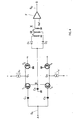
- FIG. 4 represents a preferred embodiment of the invention.
- the line signal SA applied at A is the ternary signal possibly marred by errors.
- Two capacitors C1 and C2 placed in parallel are connected on the one hand to the point A where they receive the signal SA and on the other hand to the base of the transistors Tl and T3 respectively.
- the transistors T1 and T3 play the role of current switches controlled by the input signal SA in association with the two transistors T2 and T4.
- the transistors Tl and T3 are of the pnp type while the transistors T2 and T4 are of the np n type.
- the collectors of the transistors Tl and T3 are connected at a point B each to a terminal of a capacitor C3 whose other terminal is brought to ground.
- the transmitter of transistors Tl and T3 is connected to a current source at a point G 1 and G 2 respectively.
- the point G 1 is brought to a positive potential while the point G z to a negative potential.
- the emitter of transistor T2 (resp. T4) is also connected in Gl (resp. G2) to the positive potential (resp. Negative).
- the collectors of the transistors T2 and T4 are brought to ground.
- the base of the transistors T2 and T4 is brought to a suitably chosen bias potential, for example a DC voltage as a function of the amplitude of the input signal.
- the transistors T 2 and T 4 are conductive and the transistors T 1 and T 3 are blocked.
- the transistors T 1 and T 4 become conductive and the transistors T 2 and T 3 are blocked.
- the current I o passes through the transistor T 1 and charges the capacitor C 3 .
- the transistors T 3 and T 2 are conductive and the transistors T 1 and T 4 are blocked and the capacitor C 3 discharges current I o through the transistor T 3 .
- Such integrating means make it possible to charge the capacitor C 3 at constant current I o while overcoming the amplitude of the pulses of the signal SA.
- the transistors T 1 or T 3 are conductive, the capacitor C 3 is charged or discharged by the current I o and the charge of the capacitor C 3 is proportional to the duration of the signal control pulses SA and not to their amplitude.
- At point B are connected in parallel the cathode of a diode D 1 and the anode of a diode D 2 .
- the anode of the diode D 1 is connected to a primary winding P 1 , the other terminal of which is brought to ground.
- the cathode of diode D 2 is connected to a primary winding, the other terminal of which is brought to ground.
- the two diodes D 1 and D 2 made conductive by the overshoots consecutive to the negative and positive errors respectively, constitute the detection circuit proper.
- the two windings P 1 and P 2 are the primary of a transformer Tr which includes a secondary winding X receiving the pulses transmitted by the two primary windings. These two primary windings are mounted in reverse so that one obtains at the two terminals of the secondary winding of the pulses of the same direction, rectified.
- This secondary winding X is mounted between ground and the terminal of a comparator F. The other terminal of this comparator F is brought to a reference potential. Any positive voltage overshoot is then transmitted to the output D of this comparator F in the form of a signal S D of the same type as the signal Sd of FIG. 3.
- the integration device of FIG. 4 formed by two current switches with complementary transistors charging and discharging a capacitor would also be possible in another way without departing from the error detection system of the invention.
- the device of the invention has many advantages such as low current consumption.
- the present invention has been described in the case of a bipolar code; however, the error detection device of the invention would also apply to the HDB code and to any code whose number of pulses is alternated and above all whose number of consecutive pulses of the same polarity is limited. Then the integration means would be substantially the same, but at point B the comparison means would be given for any overshoot at these n levels instead of two levels.
- the invention would also be applicable to code 4B 3T without significant modification.
Landscapes
- Engineering & Computer Science (AREA)
- Computer Networks & Wireless Communication (AREA)
- Signal Processing (AREA)
- Dc Digital Transmission (AREA)
Applications Claiming Priority (2)
| Application Number | Priority Date | Filing Date | Title |
|---|---|---|---|
| FR8018258 | 1980-08-21 | ||
| FR8018258A FR2489060A1 (fr) | 1980-08-21 | 1980-08-21 | Dispositif de detection d'erreurs d'un signal en code ternaire |
Publications (1)
| Publication Number | Publication Date |
|---|---|
| EP0047683A1 true EP0047683A1 (de) | 1982-03-17 |
Family
ID=9245322
Family Applications (1)
| Application Number | Title | Priority Date | Filing Date |
|---|---|---|---|
| EP81401282A Withdrawn EP0047683A1 (de) | 1980-08-21 | 1981-08-10 | Einrichtung zur Fehlererkennung eines ternären Signals |
Country Status (2)
| Country | Link |
|---|---|
| EP (1) | EP0047683A1 (de) |
| FR (1) | FR2489060A1 (de) |
Cited By (4)
| Publication number | Priority date | Publication date | Assignee | Title |
|---|---|---|---|---|
| EP0092216A2 (de) * | 1982-04-20 | 1983-10-26 | Siemens Aktiengesellschaft | Coderegelverletzungsprüfer für digitale Signale im AMI-Code |
| EP0092215A2 (de) * | 1982-04-20 | 1983-10-26 | Siemens Aktiengesellschaft | Regenerator für digitale Signale im AMI-Code mit einem Coderegelverletzungsprüfer |
| FR2609355A1 (fr) * | 1987-01-06 | 1988-07-08 | Rault Jean Christophe | Dispositif de detection et de correction des erreurs dans un signal numerique en code bipolaire |
| US9649985B2 (en) | 2009-09-22 | 2017-05-16 | Thule Sweden Ab | Vehicle trunk mountable bicycle rack |
Citations (1)
| Publication number | Priority date | Publication date | Assignee | Title |
|---|---|---|---|---|
| US3048819A (en) * | 1960-12-05 | 1962-08-07 | Bell Telephone Labor Inc | Detection and measurement of errors in pulse code trains |
-
1980
- 1980-08-21 FR FR8018258A patent/FR2489060A1/fr active Granted
-
1981
- 1981-08-10 EP EP81401282A patent/EP0047683A1/de not_active Withdrawn
Patent Citations (1)
| Publication number | Priority date | Publication date | Assignee | Title |
|---|---|---|---|---|
| US3048819A (en) * | 1960-12-05 | 1962-08-07 | Bell Telephone Labor Inc | Detection and measurement of errors in pulse code trains |
Non-Patent Citations (1)
| Title |
|---|
| MARCONI INSTRUMENTATION, vol. 12, no. 4, décember 1969, Herts, GB A.N. RAMSDEN: "PCM Testing techniques", pages 73-79 * |
Cited By (10)
| Publication number | Priority date | Publication date | Assignee | Title |
|---|---|---|---|---|
| EP0092216A2 (de) * | 1982-04-20 | 1983-10-26 | Siemens Aktiengesellschaft | Coderegelverletzungsprüfer für digitale Signale im AMI-Code |
| EP0092215A2 (de) * | 1982-04-20 | 1983-10-26 | Siemens Aktiengesellschaft | Regenerator für digitale Signale im AMI-Code mit einem Coderegelverletzungsprüfer |
| EP0092215A3 (en) * | 1982-04-20 | 1984-02-22 | Siemens Aktiengesellschaft | Regenerator for ami coded digital signals with a tester for coding rule violations |
| EP0092216A3 (en) * | 1982-04-20 | 1984-02-22 | Siemens Aktiengesellschaft | Tester for coding rule violations for ami coded digital signals |
| FR2609355A1 (fr) * | 1987-01-06 | 1988-07-08 | Rault Jean Christophe | Dispositif de detection et de correction des erreurs dans un signal numerique en code bipolaire |
| US9649985B2 (en) | 2009-09-22 | 2017-05-16 | Thule Sweden Ab | Vehicle trunk mountable bicycle rack |
| US9649987B2 (en) | 2009-09-22 | 2017-05-16 | Thule Sweden Ab | Locking latch on central hub for a rack arrangement mountable to a motor vehicle |
| US9751470B2 (en) | 2009-09-22 | 2017-09-05 | Thule Sweden Ab | Strap with removable hook for rack arrangement mountable to a motor vehicle |
| US10252681B2 (en) | 2009-09-22 | 2019-04-09 | Thule Sweden Ab | Splined hub with locking latch for a rack arrangement mountable to a motor vehicle |
| US10926710B2 (en) | 2009-09-22 | 2021-02-23 | Thule Sweden Ab | Vehicle trunk mountable bicycle rack |
Also Published As
| Publication number | Publication date |
|---|---|
| FR2489060B1 (de) | 1983-02-04 |
| FR2489060A1 (fr) | 1982-02-26 |
Similar Documents
| Publication | Publication Date | Title |
|---|---|---|
| EP0082791A1 (de) | Signalübertragungseinrichtung über eine Leitung die zugleich die Gleichspannungsspeisung sichert | |
| EP0116293B1 (de) | Modulationssystem für Eisenbahnstromkreise | |
| EP0570289B1 (de) | Einrichtung zur Detektion der Durchfahrt eines Fahrzeuges mittels eines passiven Transponders | |
| FR2551555A1 (fr) | Detecteur de l'intensite d'un signal, notamment radioelectrique, et circuit le comprenant | |
| EP0404002B1 (de) | Detektor für Niederfrequenz-Wechselstromsignale für eine Telefonverbindungsleitung | |
| EP0058703A1 (de) | Einrichtung zur erhöhung des dynamikbereichs an der eingangsstufe eines empfängers in einem lichtwellenleiter-informationsübertragungssystem. | |
| EP0047683A1 (de) | Einrichtung zur Fehlererkennung eines ternären Signals | |
| FR2511511A1 (fr) | Systeme de localisation de boucles et d'ouvertures dans une ligne bifilaire | |
| EP0010010B1 (de) | Anlage mit Schwelle zum Unterscheiden zwischen Weiss und Schwarz auf einem Dokument und solch eine Vorrichtung enthaltender Fernkopiersender | |
| FR2520174A1 (fr) | Systeme de transmission de signaux numeriques sur fibre optique | |
| FR2458961A1 (fr) | Procede de transmission de signaux binaires par un reseau etranger | |
| EP0362583A1 (de) | Mikrowellen-Modulator für zwei Phasenzustände : O, Pi mit sehr niedrigen Verlusten | |
| FR2584548A1 (fr) | Dispositif d'augmentation de la dynamique d'un circuit d'amplification, en particulier d'un recepteur mls de bord | |
| CA2012687A1 (fr) | Procede et dispositif de reduction du bruit sur un signal codable a plusieurs niveaux predetermines | |
| EP4213413A1 (de) | Empfangsvorrichtung, system, empfangsverfahren und lichtsignalkommunikationsverfahren | |
| EP0404001B1 (de) | Signalisierungsdetektor für Gebührensignalisierung für eine Telefonverbindungsleitung | |
| EP0613244B1 (de) | Vorrichtung mit grossen Linearität der Begrenzung einer Eigenschaft eines Signals und Verwendung der Vorrichtung in einem Radarempfänger | |
| EP0625769B1 (de) | Übertragungsschaltung für eine wesentliche Gleichspannung mit galvanischer Trennung zwischen Eingang und Ausgang | |
| EP0329525A1 (de) | Umschaltbare selbstabgleichende Filterschaltung für Runkfunksender und/oder Rundfunkempfänger | |
| FR1465628A (fr) | Perfectionnements aux circuits basculeurs | |
| FR2524741A1 (fr) | Dispositif de restitution d'informations transmises sur une fibre optique et recepteur comportant un tel dispositif | |
| EP0125984B1 (de) | Verfahren zur Regenerierung von verzerrten digitalen Signalen und Schaltungsanordnung zur Durchführung des Verfahrens | |
| FR2525839A1 (fr) | Procede de detection d'absence de signal numerique, dispositif pour la mise en oeuvre de ce procede et utilisation d'un tel dispositif | |
| FR2489058A1 (fr) | Recepteur pour systeme de transmission de signaux par rayonnement electromagnetique, notamment infrarouge | |
| FR2518855A1 (fr) | Dispositif individuel d'essais de ligne et de joncteur d'abonne integre a un joncteur electronique |
Legal Events
| Date | Code | Title | Description |
|---|---|---|---|
| PUAI | Public reference made under article 153(3) epc to a published international application that has entered the european phase |
Free format text: ORIGINAL CODE: 0009012 |
|
| AK | Designated contracting states |
Designated state(s): AT BE CH DE GB IT LU NL SE |
|
| 17P | Request for examination filed |
Effective date: 19820215 |
|
| STAA | Information on the status of an ep patent application or granted ep patent |
Free format text: STATUS: THE APPLICATION IS DEEMED TO BE WITHDRAWN |
|
| 18D | Application deemed to be withdrawn |
Effective date: 19840110 |
|
| RIN1 | Information on inventor provided before grant (corrected) |
Inventor name: DU CHAFFAUT, GUY MARIE Inventor name: LE FORT, GILBERT JEAN |