EP0047579A2 - Entlötungsvorrichtung - Google Patents
Entlötungsvorrichtung Download PDFInfo
- Publication number
- EP0047579A2 EP0047579A2 EP81303446A EP81303446A EP0047579A2 EP 0047579 A2 EP0047579 A2 EP 0047579A2 EP 81303446 A EP81303446 A EP 81303446A EP 81303446 A EP81303446 A EP 81303446A EP 0047579 A2 EP0047579 A2 EP 0047579A2
- Authority
- EP
- European Patent Office
- Prior art keywords
- fibres
- solder
- coated
- flux
- metal
- Prior art date
- Legal status (The legal status is an assumption and is not a legal conclusion. Google has not performed a legal analysis and makes no representation as to the accuracy of the status listed.)
- Granted
Links
Images
Classifications
-
- B—PERFORMING OPERATIONS; TRANSPORTING
- B23—MACHINE TOOLS; METAL-WORKING NOT OTHERWISE PROVIDED FOR
- B23K—SOLDERING OR UNSOLDERING; WELDING; CLADDING OR PLATING BY SOLDERING OR WELDING; CUTTING BY APPLYING HEAT LOCALLY, e.g. FLAME CUTTING; WORKING BY LASER BEAM
- B23K3/00—Tools, devices or special appurtenances for soldering, e.g. brazing, or unsoldering, not specially adapted for particular methods
- B23K3/08—Auxiliary devices therefor
-
- Y—GENERAL TAGGING OF NEW TECHNOLOGICAL DEVELOPMENTS; GENERAL TAGGING OF CROSS-SECTIONAL TECHNOLOGIES SPANNING OVER SEVERAL SECTIONS OF THE IPC; TECHNICAL SUBJECTS COVERED BY FORMER USPC CROSS-REFERENCE ART COLLECTIONS [XRACs] AND DIGESTS
- Y10—TECHNICAL SUBJECTS COVERED BY FORMER USPC
- Y10T—TECHNICAL SUBJECTS COVERED BY FORMER US CLASSIFICATION
- Y10T428/00—Stock material or miscellaneous articles
- Y10T428/12—All metal or with adjacent metals
- Y10T428/12424—Mass of only fibers
Definitions
- This invention relates to a solder removing device for use in absorbing, by capillary attraction, solder which has been made molten by heating when it is desired to break a soldered connection, for example in an electronic circuit.
- Solder removing wicks or braids are known (for example my U.S. patent 4 081 575) comprising fine copper wires braided together and coated with a solder flux (for example rosin) to improve the capability of the wires to be wetted by the molten solder.
- a solder flux for example rosin
- each copper wire is provided with an alloy coating.
- solder removing wicks use a considerable quantity of copper, which is discarded and can no longer be used after the wick has become filled with absorbed solder. Copper is expensive and a limited world resource, so that its substantial use in the solder removing wicks is a disadvantage of those wiaks.
- braiding machines are used. Such machines are well suited to textile making processes, but not so well suited to copper (or other metal) strands, and braiding of the metal fibres is not easy.
- a lubricant to minimise friction and wear between the copper fibres and the braiding machine. Residues of the lubricant remaining on the copper fibres have to be removed before the braid can be coated with the flux. This is to avoid interaction of the lubricant with the flux and a consequent reduction in the wetting capability of the flux, and also to avoid possible contamination of the printed circuit boards on which the wick is subsequently used leading to unwanted conductivity paths on or corrosion of the printed circuit board.
- the cleaning of the wick to remove the lubricant involves an additional process increasing the costs of manufacturing the wick.
- solder removing devices have been in the form of elongate wicks or braids.
- Modern-day trends in electronic components involve a considerable increase in the number of pins on the component, all soldered to conductive paths on the printed circuit board.
- integrated circuits commonly had 14 pins maximum, then the number increased to 16 and to-day there are microprocessor circuits with 32 or more pins.
- an appropriately shaped solder tip is applied to the pins on the soldered side of the board, to melt the solder of all pins simultaneously.
- the integrated circuit component may then be removed from the opposite side of the board, but this leaves the board with its pin apertures still filled with solder, which quickly re-solidifies. Then it is necessary to heat the solder in the pin apertures, and apply the desoldering wick to those apertures, one-by-one and this is a time consuming operation. Also, it involves putting the circuit board through repetitive heat cycles (as the heat applied to any one pin aperture will also affect the adjacent pin apertures). Such repetitive heat cycles are liable to damage the circuit board.
- an appropriate pad-shaped solder removing wick suggests itself, which could be pressed against all pins simultaneously during the first heating process (namely, the application of the shaped solder tip to effect melting of the solder of all pins simultaneously). If the pad is soft and deformable so as to adapt itself to the projecting pins it would effectively remove all solder from all pins simultaneously, with just a single application of heat. However, copper or other metal fibres are too stiff and a pad formed from them would not be satisfactory. Moreover, there would be a considerable waste of the expensive copper, because only the opposite edges of the pad, adjacent the two rows of component pins, would absorb solder, the remaining central area of the pad being unused.
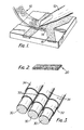
- a solder removing device comprising fibres of temperature-resistant non-metallic material which are coated with a metal rendering them more receptive to solder flux, the metallised fibres being coated with solder flux rendering them more capable of wetting with molten solder, interstices between the fibres providing for absorbing molten solder by capillary attraction.
- Suitable non-metallic materials for the fibres include, for example, high melting synthetic polymeric materials such as TEFLON (trade mark), polytetrafluoroethylene, other fluoroethylene polymers (including copolymers), VESPEL (trade mark) which is a polyimide, KAPTON (trade mark) which is a polyimide derived from pyromellitic acid, and other materials such as glass fibres. Such materials can be exposed to the temperatures of molten electronic-grade soft solder alloys.
- Du Pont technical literature states that TEFLON can be exposed to 316 0 C for short times without influence on its material properties, and fibres of this material in the form of a desoldering device in accordance with this invention can be put to even higher- temperatures, because the heated material is filled with solder and discarded.
- TEFLON fibres are available in non-filament or multi-filament form and either can be used for the de- soldering device.
- Metallisation of TEFLON is known in connection with other arts (for example to permit soldering together of two TEFLON parts in coaxial high frequency conductors) and well documented in the literature relating to TEFLON.
- the metallisation of TEFLON fibres is necessary in the desoldering device because TEFLON is itself not wetted by solder.
- the metallisation may comprise one or more layers of metal, finishing with an outer coating of copper or tin or some other metal or alloy readily wetted by molten solder.
- TEFLON may be metallised by the deposit of metal ions in a liquid phase or under vacuum by evaporation of metal actions onto the TEFLON surface.
- the TEFLON surface must be prepared, for example chemically etched or bombarded with ions or electrons.
- the non-metallic fibres may be metallised either before braiding or weaving or stranding together, or afterwards, or a first metallisation may be carried out before braiding, weaving or stranding together and a second metallisation carried out afterwards.
- the fibres need not be braided, woven or stranded together, but may instead be arranged in matted, non-woven form. In order to form a non-woven fabric of TEFLON, for example, they must be rendered less slippery so as to interlock.
- interlocking may be achieved by spraying the loose, metallised fibres (for example passing along a conveyor belt) with the flux (e.g. rosin) in a solution, with subsequent drying (see my U.S. patent 4 081 575). The rosin effectively glues the fibres together.
- Glass fibres are also an appropriate material and they also can be metallised. Technologies already exist for forming non-woven pads of glass fibres, and can be used whether the fibres are metallised prior to forming into the pad, or afterwards, or whether there are metallisation processes both beforehand and afterwards.
- a pad of non-woven glass fibres may be metallised with aluminium by vacuum deposition, then metallised with copper or tin or an alloy, and finally sprayed with or dipped in rosin flux and dried.
- Glass is a very widely available raw material, highly resistant to such temperatures found in soft soldering and chemically inert. Desoldering devices formed of this material can therefore be produced very much less expensively than corresponding devices of copper. Indeed, the device when formed from glass fibres can be used for hard soldering (with appropriate flux) because it can withstand the temperatures encountered therein.
Landscapes
- Engineering & Computer Science (AREA)
- Mechanical Engineering (AREA)
- Electric Connection Of Electric Components To Printed Circuits (AREA)
- Manufacturing Of Printed Wiring (AREA)
- Laminated Bodies (AREA)
- Preliminary Treatment Of Fibers (AREA)
Priority Applications (1)
| Application Number | Priority Date | Filing Date | Title |
|---|---|---|---|
| AT81303446T ATE7867T1 (de) | 1980-09-05 | 1981-07-27 | Entloetungsvorrichtung. |
Applications Claiming Priority (2)
| Application Number | Priority Date | Filing Date | Title |
|---|---|---|---|
| GB8028819A GB2082952B (en) | 1980-09-05 | 1980-09-05 | Solder removing device |
| GB8028819 | 1980-09-05 |
Publications (3)
| Publication Number | Publication Date |
|---|---|
| EP0047579A2 true EP0047579A2 (de) | 1982-03-17 |
| EP0047579A3 EP0047579A3 (en) | 1982-03-31 |
| EP0047579B1 EP0047579B1 (de) | 1984-06-13 |
Family
ID=10515893
Family Applications (1)
| Application Number | Title | Priority Date | Filing Date |
|---|---|---|---|
| EP81303446A Expired EP0047579B1 (de) | 1980-09-05 | 1981-07-27 | Entlötungsvorrichtung |
Country Status (6)
| Country | Link |
|---|---|
| US (1) | US4323631A (de) |
| EP (1) | EP0047579B1 (de) |
| JP (1) | JPS5779070A (de) |
| AT (1) | ATE7867T1 (de) |
| DE (1) | DE3164159D1 (de) |
| GB (1) | GB2082952B (de) |
Families Citing this family (15)
| Publication number | Priority date | Publication date | Assignee | Title |
|---|---|---|---|---|
| JPS5954461A (ja) * | 1982-09-20 | 1984-03-29 | エルンスト・スピリツク | はんだ除去装置 |
| US4923521A (en) * | 1988-10-11 | 1990-05-08 | American Telephone And Telegraph Company | Method and apparatus for removing solder |
| US5284286A (en) * | 1991-10-31 | 1994-02-08 | International Business Machines Corporation | Porous metal block for removing solder or braze from a substate and a process for making the same |
| US5219520A (en) * | 1991-10-31 | 1993-06-15 | International Business Machines Corporation | Process of making a porous metal block for removing solder or braze |
| US5305941A (en) * | 1992-12-28 | 1994-04-26 | Plato Products, Inc. | Desoldering wick |
| USH1306H (en) | 1993-01-21 | 1994-05-03 | The United States Of America As Represented By The Secretary Of The Army | Method of using an improved solder to bridge a nonmetallic gap between metallic surfaces, said improved solder, and an improved solder connection to bridge a nonmetallic gap between metallic surfaces |
| US5458281A (en) * | 1994-06-30 | 1995-10-17 | International Business Machines Corporation | Method for removing meltable material from a substrate |
| US5901898A (en) * | 1997-05-14 | 1999-05-11 | Easy-Braid Company | System for removing solder |
| US5909838A (en) * | 1997-11-04 | 1999-06-08 | Ibm | Method of solder removal |
| US7285173B2 (en) * | 2003-11-21 | 2007-10-23 | Illinois Tool Works, Inc. | Desoldering systems and processes |
| US7134590B2 (en) * | 2004-03-16 | 2006-11-14 | Moon Gul Choi | Desoldering sheath |
| US7780058B2 (en) * | 2008-02-27 | 2010-08-24 | Siuyoung Yao | Braided solder |
| US8413320B2 (en) * | 2011-01-28 | 2013-04-09 | Raytheon Company | Method of gold removal from electronic components |
| US10269762B2 (en) * | 2015-10-29 | 2019-04-23 | Taiwan Semiconductor Manufacturing Company, Ltd. | Rework process and tool design for semiconductor package |
| US10307850B2 (en) * | 2017-08-24 | 2019-06-04 | Micron Technology, Inc. | Solder removal from semiconductor devices |
Family Cites Families (6)
| Publication number | Priority date | Publication date | Assignee | Title |
|---|---|---|---|---|
| US2616165A (en) * | 1947-01-18 | 1952-11-04 | Everett D Mccurdy | Electrode for electrolytic devices and methods of making same |
| US3627191A (en) * | 1968-03-18 | 1971-12-14 | Jesse Carl Hood Jr | Solder wick |
| JPS4867025U (de) * | 1971-12-06 | 1973-08-25 | ||
| US4081575A (en) * | 1976-04-30 | 1978-03-28 | Ernst Spirig | Method of flux coating metal wick |
| US4164606A (en) * | 1977-11-08 | 1979-08-14 | Ernst Spirig | Tinned copper braids for solder removing |
| US4194705A (en) * | 1978-09-29 | 1980-03-25 | Ernst Spirig | Desoldering wick package and improved bobbin utilized therein |
-
1980
- 1980-09-05 GB GB8028819A patent/GB2082952B/en not_active Expired
- 1980-10-27 US US06/201,228 patent/US4323631A/en not_active Expired - Lifetime
-
1981
- 1981-07-27 AT AT81303446T patent/ATE7867T1/de active
- 1981-07-27 EP EP81303446A patent/EP0047579B1/de not_active Expired
- 1981-07-27 DE DE8181303446T patent/DE3164159D1/de not_active Expired
- 1981-09-05 JP JP56140224A patent/JPS5779070A/ja active Granted
Also Published As
| Publication number | Publication date |
|---|---|
| ATE7867T1 (de) | 1984-06-15 |
| JPH0129629B2 (de) | 1989-06-13 |
| EP0047579A3 (en) | 1982-03-31 |
| EP0047579B1 (de) | 1984-06-13 |
| GB2082952B (en) | 1984-04-18 |
| JPS5779070A (en) | 1982-05-18 |
| US4323631A (en) | 1982-04-06 |
| GB2082952A (en) | 1982-03-17 |
| DE3164159D1 (en) | 1984-07-19 |
Similar Documents
| Publication | Publication Date | Title |
|---|---|---|
| EP0047579B1 (de) | Entlötungsvorrichtung | |
| CA1187678A (en) | Method of bonding electronic components | |
| US5282565A (en) | Solder bump interconnection formed using spaced solder deposit and consumable path | |
| US6229209B1 (en) | Chip carrier | |
| US5271548A (en) | Method for applying solder to and mounting components on printed circuit boards | |
| US6871776B2 (en) | Manufacture of solid-solder-deposit PCB utilizing electrically heated wire mesh | |
| WO2003052875A1 (de) | Aufbau- und verbindungstechnik in textilen strukturen | |
| JP2004207232A (ja) | 半田貯蔵移動装置及び工程 | |
| US5541368A (en) | Laminated multi chip module interconnect apparatus | |
| US4345814A (en) | Solder-bearing lead having solder flow-control stop means | |
| US6548790B1 (en) | Apparatus for manufacturing solid solder deposit PCBs | |
| EP0915641B1 (de) | Oberflächenmontierte Anordnung von elektronischen Bauteilen | |
| USRE32086E (en) | Solder removing device | |
| KR960003728B1 (ko) | 지연식 리플로우 합금 혼합물 납땜 페이스트 및 이의 제조 방법 | |
| EP1866961A2 (de) | Mikro-löt-topf | |
| US7279409B2 (en) | Method for forming multi-layer bumps on a substrate | |
| EP0878262B1 (de) | System zum Entfernen von Lötmaterial | |
| US5833128A (en) | Flux-free contacting of components | |
| JPH07193365A (ja) | 半田コーティング方法及び該コーティングにおける使用に適切な半田ペースト | |
| KR100352202B1 (ko) | 땜납-코팅방법및상기방법에사용되는땜납페이스트 | |
| KR101324629B1 (ko) | 무연 솔더제거용 브레이드 | |
| US20010052536A1 (en) | Method and apparatus for making an electrical device | |
| US4141028A (en) | Contact clip | |
| EP0102426B1 (de) | Vorrichtung zum Entlöten | |
| JPH0467662A (ja) | パッケージリードピン |
Legal Events
| Date | Code | Title | Description |
|---|---|---|---|
| PUAI | Public reference made under article 153(3) epc to a published international application that has entered the european phase |
Free format text: ORIGINAL CODE: 0009012 |
|
| PUAL | Search report despatched |
Free format text: ORIGINAL CODE: 0009013 |
|
| AK | Designated contracting states |
Designated state(s): AT BE CH DE FR GB IT LU NL SE |
|
| AK | Designated contracting states |
Designated state(s): AT BE CH DE FR GB IT LU NL SE |
|
| 17P | Request for examination filed |
Effective date: 19820921 |
|
| ITF | It: translation for a ep patent filed | ||
| GRAA | (expected) grant |
Free format text: ORIGINAL CODE: 0009210 |
|
| AK | Designated contracting states |
Designated state(s): AT BE CH DE FR GB IT LI LU NL SE |
|
| REF | Corresponds to: |
Ref document number: 7867 Country of ref document: AT Date of ref document: 19840615 Kind code of ref document: T |
|
| REF | Corresponds to: |
Ref document number: 3164159 Country of ref document: DE Date of ref document: 19840719 |
|
| PGFP | Annual fee paid to national office [announced via postgrant information from national office to epo] |
Ref country code: CH Payment date: 19840723 Year of fee payment: 4 |
|
| PG25 | Lapsed in a contracting state [announced via postgrant information from national office to epo] |
Ref country code: LU Free format text: LAPSE BECAUSE OF NON-PAYMENT OF DUE FEES Effective date: 19840731 |
|
| ET | Fr: translation filed | ||
| PGFP | Annual fee paid to national office [announced via postgrant information from national office to epo] |
Ref country code: SE Payment date: 19840930 Year of fee payment: 4 Ref country code: BE Payment date: 19840930 Year of fee payment: 4 |
|
| PLBE | No opposition filed within time limit |
Free format text: ORIGINAL CODE: 0009261 |
|
| STAA | Information on the status of an ep patent application or granted ep patent |
Free format text: STATUS: NO OPPOSITION FILED WITHIN TIME LIMIT |
|
| 26N | No opposition filed | ||
| PGFP | Annual fee paid to national office [announced via postgrant information from national office to epo] |
Ref country code: AT Payment date: 19850722 Year of fee payment: 5 |
|
| PG25 | Lapsed in a contracting state [announced via postgrant information from national office to epo] |
Ref country code: AT Effective date: 19860727 |
|
| PG25 | Lapsed in a contracting state [announced via postgrant information from national office to epo] |
Ref country code: SE Effective date: 19860728 |
|
| PG25 | Lapsed in a contracting state [announced via postgrant information from national office to epo] |
Ref country code: BE Effective date: 19860731 |
|
| PGFP | Annual fee paid to national office [announced via postgrant information from national office to epo] |
Ref country code: NL Payment date: 19860731 Year of fee payment: 6 |
|
| BERE | Be: lapsed |
Owner name: SPIRIG ERNST Effective date: 19860731 |
|
| PG25 | Lapsed in a contracting state [announced via postgrant information from national office to epo] |
Ref country code: LI Effective date: 19870731 Ref country code: CH Effective date: 19870731 |
|
| PG25 | Lapsed in a contracting state [announced via postgrant information from national office to epo] |
Ref country code: NL Effective date: 19880201 |
|
| NLV4 | Nl: lapsed or anulled due to non-payment of the annual fee | ||
| REG | Reference to a national code |
Ref country code: CH Ref legal event code: PL |
|
| EUG | Se: european patent has lapsed |
Ref document number: 81303446.9 Effective date: 19870609 |
|
| PGFP | Annual fee paid to national office [announced via postgrant information from national office to epo] |
Ref country code: FR Payment date: 19950711 Year of fee payment: 15 |
|
| PGFP | Annual fee paid to national office [announced via postgrant information from national office to epo] |
Ref country code: GB Payment date: 19950717 Year of fee payment: 15 |
|
| PGFP | Annual fee paid to national office [announced via postgrant information from national office to epo] |
Ref country code: DE Payment date: 19950725 Year of fee payment: 15 |
|
| PG25 | Lapsed in a contracting state [announced via postgrant information from national office to epo] |
Ref country code: GB Effective date: 19960727 |
|
| GBPC | Gb: european patent ceased through non-payment of renewal fee |
Effective date: 19960727 |
|
| PG25 | Lapsed in a contracting state [announced via postgrant information from national office to epo] |
Ref country code: FR Effective date: 19970328 |
|
| PG25 | Lapsed in a contracting state [announced via postgrant information from national office to epo] |
Ref country code: DE Effective date: 19970402 |
|
| REG | Reference to a national code |
Ref country code: FR Ref legal event code: ST |