EP0046578A2 - Power thyristor - Google Patents
Power thyristor Download PDFInfo
- Publication number
- EP0046578A2 EP0046578A2 EP81106493A EP81106493A EP0046578A2 EP 0046578 A2 EP0046578 A2 EP 0046578A2 EP 81106493 A EP81106493 A EP 81106493A EP 81106493 A EP81106493 A EP 81106493A EP 0046578 A2 EP0046578 A2 EP 0046578A2
- Authority
- EP
- European Patent Office
- Prior art keywords
- electrode
- portions
- semiconductor
- layer
- sub
- Prior art date
- Legal status (The legal status is an assumption and is not a legal conclusion. Google has not performed a legal analysis and makes no representation as to the accuracy of the status listed.)
- Granted
Links
- 239000004065 semiconductor Substances 0.000 claims abstract description 69
- 238000009751 slip forming Methods 0.000 claims description 3
- 230000003321 amplification Effects 0.000 description 4
- 238000003199 nucleic acid amplification method Methods 0.000 description 4
- 230000017525 heat dissipation Effects 0.000 description 2
- 238000000034 method Methods 0.000 description 2
- 238000010586 diagram Methods 0.000 description 1
Images


Classifications
-
- H—ELECTRICITY
- H01—ELECTRIC ELEMENTS
- H01L—SEMICONDUCTOR DEVICES NOT COVERED BY CLASS H10
- H01L29/00—Semiconductor devices adapted for rectifying, amplifying, oscillating or switching, or capacitors or resistors with at least one potential-jump barrier or surface barrier, e.g. PN junction depletion layer or carrier concentration layer; Details of semiconductor bodies or of electrodes thereof ; Multistep manufacturing processes therefor
- H01L29/02—Semiconductor bodies ; Multistep manufacturing processes therefor
- H01L29/06—Semiconductor bodies ; Multistep manufacturing processes therefor characterised by their shape; characterised by the shapes, relative sizes, or dispositions of the semiconductor regions ; characterised by the concentration or distribution of impurities within semiconductor regions
- H01L29/08—Semiconductor bodies ; Multistep manufacturing processes therefor characterised by their shape; characterised by the shapes, relative sizes, or dispositions of the semiconductor regions ; characterised by the concentration or distribution of impurities within semiconductor regions with semiconductor regions connected to an electrode carrying current to be rectified, amplified or switched and such electrode being part of a semiconductor device which comprises three or more electrodes
- H01L29/083—Anode or cathode regions of thyristors or gated bipolar-mode devices
- H01L29/0839—Cathode regions of thyristors
-
- H—ELECTRICITY
- H01—ELECTRIC ELEMENTS
- H01L—SEMICONDUCTOR DEVICES NOT COVERED BY CLASS H10
- H01L29/00—Semiconductor devices adapted for rectifying, amplifying, oscillating or switching, or capacitors or resistors with at least one potential-jump barrier or surface barrier, e.g. PN junction depletion layer or carrier concentration layer; Details of semiconductor bodies or of electrodes thereof ; Multistep manufacturing processes therefor
- H01L29/66—Types of semiconductor device ; Multistep manufacturing processes therefor
- H01L29/68—Types of semiconductor device ; Multistep manufacturing processes therefor controllable by only the electric current supplied, or only the electric potential applied, to an electrode which does not carry the current to be rectified, amplified or switched
- H01L29/70—Bipolar devices
- H01L29/74—Thyristor-type devices, e.g. having four-zone regenerative action
- H01L29/7428—Thyristor-type devices, e.g. having four-zone regenerative action having an amplifying gate structure, e.g. cascade (Darlington) configuration
Abstract
Description
- The present invention relates to a semiconductor device, and more particularly to a power thyristor with a large critical rate of rise of on-state current (di/dt) and free from a finger voltage phenomenon.
- There has been known a thyristor with a steep rise characteristic of an ON current and a large critical rate of rise of on-state current (di/dt). The prior art thyristor has a structure as shown in Figs. 1 and 2, for example. The thyristor shown in those figures is made of a
first semiconductor layer 12 of N conductivity type, second andthird semiconductor layers first layer 12, amain emitter region 18 of N conductivity type and anauxiliary emitter region 20 of the same type, both being formed in thesecond layer 12, acathode electrode 22 formed on themain emitter region 18, agate electrode 24 formed on thesecond semiconductor layer 14, ananode electrode 26 formed on thethird semiconductor layer 16, and anauxiliary electrode 28 formed on thesecond semiconductor layer 14, being disposed along an outer periphery of thecathode electrode 22. Thecathode electrode 22 and theN region 18 cooperatively form an emitter section of a main thyristor element, while theauxiliary electrode 28 and theauxiliary emitter region 18 make up an emitter section of an auxiliary thyristor element. The thyristor with such a structure as shown in Figs. 1 and 2 operates in such a way that a gate current ① flowing through thegate electrode 24 first turns on the auxiliary thyristor, and a turn-on current ② flows into the main thyristor element in the form of atrigger current ③ for the main thyristor element thereby turning on the main thyristor element. Thus, the prior art thyristor makes use of a called amplification gate function. Therefore, the trigger current ③ to the main thyristor element is large, so that an initial turn-on region of the main thyristor element is wide. This provides an abrupt rise of the ON current and a large critical rate of rise of on-state current (di/dt). In the prior thyristor as shown in Figs. 1 and 2, the turn-on of the main thyristor element is performed through two steps as described . above. In the course of the two-step turn-on process, a finger voltage Vfin phenomenon takes place as shown in Fig. 3. The finger voltage phenomenon offers no problem in the use of a single thyristor or when two or more parallel-connected thyristors are turned on with a high voltage applied to between the anode and cathode. However, the finger voltage phenomenon is problematic when two or more parallel-connected thyristors are turned on when a low voltage is applied therebetween. - To further discuss the finger voltage phenomenon, a simple model circuit will be used in which two thyristors SCR1 and SCR2 each having the structure as shown in Figs. 1 and 2 are inserted between terminals P and Q, being respectively connected at the cathodes to associative resistors, and at the anodes together to an inductance L.
- Assume that, in the model, a total current of 6,000 A flows through a P-Q path, and that the current equally shunts into the two thyristors SCR1 and SCR2. On this assumption, 3,000 A current flows into each of the thyristors. Even if trigger currents are concurrently fed to the two thyristors SCR1 and SCR2, only one of the thyristors is turned on when there is non-coincidence between the finger voltages of the thyristors SCR1 and SCR2, so long as the resistances of the resistors R1 and R2 are properly selected allowing for the finger voltages. Assuming that the 3,000 A current flows into the thyristor SCR1, following the turn-on of the thyristor SCR1, a voltage drop VAB as the sum of a voltage drop across the thyristor SCR1 at the time of the 3,000 A current passage through the thyristor SCR1 and a voltage drop across the resistor R1, appears between junction points A and B.
- The thyristor SCR1 has a voltage vs. current characteristic as shown in Fig. 3. The voltage drop across the thyristor SCR1 is 1.5 V when the 3,000 A current flows therethrough. The resistance of the resistor R1 is 0.2 mΩ. The voltage drop VAB is
-

- Nevertheless, the conventional thyristors have been unsucceeded in reducing the finger voltage Vfin to a desired degree or a negligible one.
- For the background reason, the present invention has an object to provide a semiconductor device with a remarkably small finger voltage and a large critical rate of rise of on-state current (di/dt).
- According to the present invention, there is provided a semiconductor device comprising a semiconductor body having a first semiconductor layer of a first conductivity type, second and third semiconductor layers of a second conductivity type formed contacting with both major surfaces of the first semiconductor layer, and first and second semiconductor regions of the first conductivity type formed in the second layer, a cathode electrode having first and second portions provided on the first region, a gate electrode provided on the second layer, an anode electrode provided on the third layer, an auxiliary electrode consisting of two first portions and one second portion connected at ends respectively to the first portions, said first portions being formed on said second region and having free ends spaced from each other, and said second portion formed on said second layer and extenting along the periphery of the first portion of said cathode electrode, and the second portion of the cathode electrode and the first portions of the auxiliary electrode being disposed in an area between the gate electrode and the cathode electrode where a gate current flows.
- This invention can be more fully understood from the following detailed description when taken in conjunction with the accompanying drawings, in which:
- Fig. 1 is a plan view of a leading portion in a structure of a prior thyristor;
- Fig. 2 is a cross sectional view taken on line II-II and as viewed in an arrow direction in Fig. 1;
- Fig. 3 is a voltage vs. current characteristic curve of the thyristor with a structure as shown in Figs. 1 and 2;
- Fig. 4 is a circuit diagram of a model circuit having two parallel-connected thyristors having a structure as shown in Figs. 1 and 2;
- Fig. 5 is a plan view of an embodiment of a semiconductor device according to the present invention;
- Fig. 6 is a cross sectional view taken on line VI-VI in Fig. 5 and as viewed in an arrow direction;
- Fig. 7 is a cross sectional view taken on line VII-VII in Fig. 5 and as viewed in an arrow direction;
- Fig. 8 is a graphical representation of a voltage-current characteristic curve of the semiconductor device shown in Figs. 5, 6 and 7, which has no finger voltage phenomenon;
- Fig. 9A is a graphical representation of a gate current of the thyristor;
- Fig. 9B is a graphical representation of variations of a voltage between the anode and the cathode and a critical rate of rise of on-state current (di/dt) at the time of the turn-on of the thyristor;
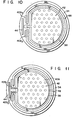
- Fig. 10 is a plan view of another embodiment of a semiconductor device according to the present invention; and
- Fig. 11 is a plan view of yet another embodiment of a semiconductor device according to the present invention.
- An embodiment of a semiconductor device according to the present invention will be described referring to Figs. 5, 6 and 7. A
first semiconductor layer 32 of N conductivity type, for example, is sandwiched at second andthird semiconductor layers main emitter region 38 of N conductivity type and anauxiliary emitter region 40 of the same conductivity type, which are continuous, are formed in thesecond semiconductor layer 34.Semiconductor layers semiconductor regions cathode electrode 42 is formed on themain emitter region 38. Agate electrode 44 is disposed on thesecond semiconductor layer 34, facing thecathode electrode 42 with theauxiliary region 40 interposed therebetween. Thecathode electrode 42 is comprised of the firstmain portion 42A andsecond portion 42B extending from the first portion.Anode electrode 46 is layered on the lower surface of thethird semiconductor layer 36. - On the
P layer 34 andauxiliary emitter region 40 anauxiliary electrode 48 is disposed. Theelectrode 48 consists of twofirst portions second portion 48B connected at ends respectively to thefirst portions first portions P layer 34 and partly on theauxiliary emitter region 40 and between thecathode electrode 42 and thegate electrode 44 and has their free.ends spaced form each other. Thesecond portion 48B is formed on theP layer 34, and extending along the periphery of thecathode electrode 42 formed on theP layer 34. - The thyristor of Figs. 5, 6 and 7 differs from the prior art thyristor in that the
cathode portion 42B of thecathode electrode 42 lies between the free ends of thefirst portions auxiliary electrode 48 and in face-to-face relation to thegate electrode 44. In other words, an essential point of the present embodiment resides in that a portion of the emitter section of the main thyristor element, i.e. a region defined by thecathode electrode 42, and an emitter section of the auxiliary thyristor element, i.e. regions defined by theportions auxiliary electrode 48, are disposed in a region where a gate current flows into a path between thegate electrode 44 and thecathode electrode 42. - The operation of the semiconductor device as described above will be described. Description will first be given about the case where thyristor is turned on in a state that a low voltage is applied between the anode and cathode of the thyristor. In this case, a gate current ① is fed to the thyristor by way of a
gate electrode 44. In response to the gate current, that portion of the main thyristor element which is close to thegate electrode 44 is turned on and current ② starts to flow. The current ② then spreads from the portion of the main thyristor element toward the entire of the main thyristor element. As a result, the main thyristor is entirely turned on and current O3 flows into the entire main thyristor element. In this way, the thyristor shown in Figs. 5 to 7 is turned on. Simultaneously, the supply of the gate current ① also turns on the auxiliary thyristor element, so that current ④ starts to flow into the auxiliary thyristor element. If the current ④ should shift to the main thyristor element at the time of the low voltage application, the problem of the prior art thyristor would arise. In the thyristor of the present embodiment, however, when a low voltage is applied, the current ④ never shifts to the main thyristor element for the following reason. In the semiconductor device of the amplification gate type, a lateral impedance between the main thyristor element and the auxiliary thyristor element is selected at a relatively large value in order to enhance the amplification gate function. Therefore, an insufficient potential difference is produced between the main and auxiliary thyristor elements at the time of the low voltage application, that is, when a potential difference between the anode and the cathode is small. Accordingly, the current ④ has an amplitude insufficient to turn on the main thyristor. The current, having flowed into the auxiliary thyristor element, flows through thesecond portion 42B of thecathode electrode 42, and then spreads into the entire area of the main thyristor element, with the result that the potential at the emitter of the main thyristor element substantially drops. As a consequence, the current ④ flowing into the main thyristor element disappears (before it shifts to the main thyristor element). - For this reason, the thyristor according to the present embodiment substantially eliminates the finger voltage phenomenon, as evident from the voltage-current characteristic curve of Fig. 8, and hence is free from the problem by the finger voltage phenomenon.
- Now it will be described how the thyristor operates when it is turned on with a high voltage applied between its anode and its cathode. Also in this case, the main thyristor element is partially turned on by feeding the gate current ① into the thyristor, as in the case of the low voltage application. With the start of the flow of the current ②, the auxiliary thyristor element is also turned on and the current ④ flows into the auxiliary thyristor element. The current @ flows as the current @ into the main thyristor element, thereby turning on the whole main thyristor element. At this point, the thyristor shown in Figs. 5 to 7 is turned on. As a result, the current ⑥ begin to flow into the whole main thyristor element. At this time, the potential of the auxiliary thyristor element abruptly falls off so that a high voltage of several hundreds, for example, is applied to between the main and auxiliary thyristor elements, thereby quickly turning on the main thyristor element. The current ② flowing into the portion of the main thyristor will spread into the entire area of the main thyristor element, but the spreading of the current ② is slow, that is, a delay time td (Fig. 9B) is long, because of small lateral resistance. Therefore, when the thyristor is turned on under the condition of the high voltage application, the current spreads from the auxiliary thyristor element to the main thyristor element, resulting in a large critical rate of rise of on-state current (di/dt).
- As seen from the foregoing description, the present embodiment according to the present invention provides a thyristor which produces a negligible finger voltage phenomenon when the thyristor is turned on under the low voltage application condition and provides a high critical rate of rise of on-state current (di/dt) when the thyristor is turned on under the high voltage application condition.
- According to an experiment conducted by the inventors in the present patent application, the thyristor of the present embodiment had: Vfin ≦ 1.5 V and critical rate of rise of on-state current (di/dt) ≧ 350 A/ps when voltage of 4,000 V is applied between the anode and the cathode. With such a structure of the thyristor of the present embodiment, an arrangement of two or more parallel-connected thyristors does not suffer from the problem of the prior art thyristor, and requires no series-connected resistors Rl and R2. No need of the resistors R1 and R2 eliminates the power loss by the resistors and the heat dissipation process, thereby realizing the miniaturization of the whole semiconductor device.
- Fig. 9A plots a gate current which is constant with respect to time. Fig. 9B plots a voltage drop across the anode-cathode path and a critical rate of rise of on-state current (di/dt) with respect to time when the thyristor is turned on by the gate current of . Fig. 9A under the low voltage application condition. The delay time td is defined by a period from the time that the gate current is supplied to the time that the voltage drop falls by 10% of the maximum value Vmax, that is, to 90% of the maximum value Vmax.
- Turning now to Figs. 10 and 11, there are shown other embodiments of a semiconductor device according to the present invention. In the embodiments shown in Figs. 10 and 11, like symbols are used to designate like or equivalent portions in Figs. 5 to 7 for simplicity of explanation.
- While, in the embodiment shown in Figs. 5 to 7, the
main emitter region 38 and theauxiliary emitter region 40 are continuously formed, those regions are separated from each other in the embodiment of Fig. 10. In this embodiment, the auxiliary emitter region is divided into two portions 40Al and 40 A2. - In the embodiment shown in Fig. 11, two
portions cathode electrode 42 lie between the free ends of thefirst portions auxiliary electrode 48, while thecathode electrode 42 has one extendingportion 42B in the embodiment shown in Figs. 5 to 7. - Also the embodiments shown in Figs. 10 and 11 can attain the effects similar to those by the embodiment shown in Figs. 5 to 7.
- Although the present invention is applied for the thyristor in the embodiments shown in Figs. 5 to 7, 10 and 11, the present invention is applicable for any semiconductor devices if those are of the so-called amplification gate type. The embodiment shown in Figs. 5 to 7 employs the N conductivity type for the first semiconductor layer, but it can use the P conductivity type semiconductor in place of the N conductivity type one. In such a case, the conductivity type of the remaining semiconductor layers and regions must of course be changed to the opposite conductivity type.
- In the embodiments of Figs. 5, 10 and 11, the second portion of the
cathode electrode 42 may not be necessarily provided. In the embodiment of Fig. 10, the second portion of thecathode electrode 42 may not be provided and thegate electrode 44 may comprise a first portion extending substantially along the first portions of theauxiliary electrode 48 and a second portion being formed between the two first portions of theauxiliary electrode 48. The second portion of thegate electrode 44 does not contact the first portions of theauxiliary electrode 48. The second portion of thegate electrode 44 also does not contact thecathode electrode 42. - It should be understood that the present invention may be changed, modified or altered within the scope of the appended claims.
Claims (10)
Applications Claiming Priority (2)
| Application Number | Priority Date | Filing Date | Title |
|---|---|---|---|
| JP115391/80 | 1980-08-22 | ||
| JP55115391A JPS5739574A (en) | 1980-08-22 | 1980-08-22 | Semiconductor device |
Publications (3)
| Publication Number | Publication Date |
|---|---|
| EP0046578A2 true EP0046578A2 (en) | 1982-03-03 |
| EP0046578A3 EP0046578A3 (en) | 1983-06-22 |
| EP0046578B1 EP0046578B1 (en) | 1985-12-04 |
Family
ID=14661380
Family Applications (1)
| Application Number | Title | Priority Date | Filing Date |
|---|---|---|---|
| EP81106493A Expired EP0046578B1 (en) | 1980-08-22 | 1981-08-20 | Power thyristor |
Country Status (5)
| Country | Link |
|---|---|
| US (1) | US4445133A (en) |
| EP (1) | EP0046578B1 (en) |
| JP (1) | JPS5739574A (en) |
| CA (1) | CA1154173A (en) |
| DE (1) | DE3173128D1 (en) |
Cited By (7)
| Publication number | Priority date | Publication date | Assignee | Title |
|---|---|---|---|---|
| GB2132327A (en) * | 1982-12-14 | 1984-07-04 | Apv Co Ltd | Heat transfer apparatus |
| EP0146040A2 (en) * | 1983-12-15 | 1985-06-26 | STMicroelectronics S.r.l. | Controlled electronic switching device for the suppression of transients |
| WO1995024554A2 (en) * | 1994-03-09 | 1995-09-14 | Cooper Industries, Inc. | A turbine engine ignition exciter circuit |
| US5656966A (en) * | 1994-03-09 | 1997-08-12 | Cooper Industries, Inc. | Turbine engine ignition exciter circuit including low voltage lockout control |
| US5970324A (en) * | 1994-03-09 | 1999-10-19 | Driscoll; John Cuervo | Methods of making dual gated power electronic switching devices |
| US5981982A (en) * | 1994-03-09 | 1999-11-09 | Driscoll; John Cuervo | Dual gated power electronic switching devices |
| US7355300B2 (en) | 2004-06-15 | 2008-04-08 | Woodward Governor Company | Solid state turbine engine ignition exciter having elevated temperature operational capability |
Families Citing this family (2)
| Publication number | Priority date | Publication date | Assignee | Title |
|---|---|---|---|---|
| JP2011151063A (en) * | 2010-01-19 | 2011-08-04 | Sansha Electric Mfg Co Ltd | Thyristor |
| JP5777761B2 (en) * | 2014-03-19 | 2015-09-09 | 株式会社三社電機製作所 | Thyristor |
Citations (4)
| Publication number | Priority date | Publication date | Assignee | Title |
|---|---|---|---|---|
| US3990090A (en) * | 1973-04-18 | 1976-11-02 | Hitachi, Ltd. | Semiconductor controlled rectifier |
| DE2625009A1 (en) * | 1975-06-04 | 1976-12-23 | Hitachi Ltd | THYRISTOR |
| DE2809564A1 (en) * | 1977-03-09 | 1978-09-14 | Hitachi Ltd | CONTROLLED SEMI-CONDUCTOR RECTIFIER |
| DE2912242A1 (en) * | 1978-03-31 | 1979-10-04 | Tokyo Shibaura Electric Co | SEMI-CONDUCTOR DEVICE |
Family Cites Families (10)
| Publication number | Priority date | Publication date | Assignee | Title |
|---|---|---|---|---|
| US2980832A (en) * | 1959-06-10 | 1961-04-18 | Westinghouse Electric Corp | High current npnp switch |
| NL6408263A (en) * | 1964-07-18 | 1966-01-19 | ||
| US3486088A (en) * | 1968-05-22 | 1969-12-23 | Nat Electronics Inc | Regenerative gate thyristor construction |
| US3579060A (en) * | 1969-03-21 | 1971-05-18 | Gen Electric | Thyristor with improved current and voltage handling characteristics |
| US3622845A (en) * | 1969-05-01 | 1971-11-23 | Gen Electric | Scr with amplified emitter gate |
| US3796850A (en) * | 1973-05-31 | 1974-03-12 | Westinghouse Electric Corp | Pan detector for induction heating cooking unit |
| US4086612A (en) * | 1973-06-12 | 1978-04-25 | Siemens Aktiengesellschaft | Thyristor |
| JPS5632528B2 (en) * | 1973-06-27 | 1981-07-28 | ||
| JPS5942991B2 (en) * | 1977-05-23 | 1984-10-18 | 株式会社日立製作所 | thyristor |
| JPS584827B2 (en) * | 1977-07-20 | 1983-01-27 | 株式会社日立製作所 | thyristor |
-
1980
- 1980-08-22 JP JP55115391A patent/JPS5739574A/en active Granted
-
1981
- 1981-08-20 US US06/294,750 patent/US4445133A/en not_active Expired - Lifetime
- 1981-08-20 DE DE8181106493T patent/DE3173128D1/en not_active Expired
- 1981-08-20 EP EP81106493A patent/EP0046578B1/en not_active Expired
- 1981-08-21 CA CA000384419A patent/CA1154173A/en not_active Expired
Patent Citations (4)
| Publication number | Priority date | Publication date | Assignee | Title |
|---|---|---|---|---|
| US3990090A (en) * | 1973-04-18 | 1976-11-02 | Hitachi, Ltd. | Semiconductor controlled rectifier |
| DE2625009A1 (en) * | 1975-06-04 | 1976-12-23 | Hitachi Ltd | THYRISTOR |
| DE2809564A1 (en) * | 1977-03-09 | 1978-09-14 | Hitachi Ltd | CONTROLLED SEMI-CONDUCTOR RECTIFIER |
| DE2912242A1 (en) * | 1978-03-31 | 1979-10-04 | Tokyo Shibaura Electric Co | SEMI-CONDUCTOR DEVICE |
Cited By (12)
| Publication number | Priority date | Publication date | Assignee | Title |
|---|---|---|---|---|
| GB2132327A (en) * | 1982-12-14 | 1984-07-04 | Apv Co Ltd | Heat transfer apparatus |
| EP0146040A2 (en) * | 1983-12-15 | 1985-06-26 | STMicroelectronics S.r.l. | Controlled electronic switching device for the suppression of transients |
| US4614962A (en) * | 1983-12-15 | 1986-09-30 | Sgs-Ates Componenti Elettronici S.P.A. | Controlled electronic switching device for the suppression of transients |
| EP0146040A3 (en) * | 1983-12-15 | 1987-09-02 | Sgs-Ates Componenti Elettronici S.P.A. | Controlled electronic switching device for the suppression of transients |
| WO1995024554A2 (en) * | 1994-03-09 | 1995-09-14 | Cooper Industries, Inc. | A turbine engine ignition exciter circuit |
| WO1995024554A3 (en) * | 1994-03-09 | 1995-11-30 | Cooper Ind Inc | A turbine engine ignition exciter circuit |
| US5592118A (en) * | 1994-03-09 | 1997-01-07 | Cooper Industries, Inc. | Ignition exciter circuit with thyristors having high di/dt and high voltage blockage |
| US5656966A (en) * | 1994-03-09 | 1997-08-12 | Cooper Industries, Inc. | Turbine engine ignition exciter circuit including low voltage lockout control |
| US5852381A (en) * | 1994-03-09 | 1998-12-22 | Cooper Industries, Inc. | Turbine engine ignition exciter circuit including low voltage lockout control |
| US5970324A (en) * | 1994-03-09 | 1999-10-19 | Driscoll; John Cuervo | Methods of making dual gated power electronic switching devices |
| US5981982A (en) * | 1994-03-09 | 1999-11-09 | Driscoll; John Cuervo | Dual gated power electronic switching devices |
| US7355300B2 (en) | 2004-06-15 | 2008-04-08 | Woodward Governor Company | Solid state turbine engine ignition exciter having elevated temperature operational capability |
Also Published As
| Publication number | Publication date |
|---|---|
| DE3173128D1 (en) | 1986-01-16 |
| EP0046578B1 (en) | 1985-12-04 |
| US4445133A (en) | 1984-04-24 |
| JPS5739574A (en) | 1982-03-04 |
| JPS6155260B2 (en) | 1986-11-27 |
| EP0046578A3 (en) | 1983-06-22 |
| CA1154173A (en) | 1983-09-20 |
Similar Documents
| Publication | Publication Date | Title |
|---|---|---|
| US4443810A (en) | Gate turn-off amplified thyristor with non-shorted auxiliary anode | |
| EP0046578A2 (en) | Power thyristor | |
| US4243999A (en) | Gate turn-off thyristor | |
| US4083063A (en) | Gate turnoff thyristor with a pilot scr | |
| US3265909A (en) | Semiconductor switch comprising a controlled rectifier supplying base drive to a transistor | |
| SE455552B (en) | SEMICONDUCTOR DEVICE INCLUDING AN OVERVOLTAGE CIRCUIT | |
| US3967294A (en) | PNPN semiconductor device | |
| JP2004356622A (en) | Junction type electronic component and integrated electric power equipment comprising electronic component | |
| US3401318A (en) | Switching element having accurately set threshold potential | |
| US6664591B2 (en) | Insulated gate semiconductor device | |
| US4195306A (en) | Gate turn-off thyristor | |
| US4471372A (en) | FET Controlled Triac | |
| US4291325A (en) | Dual gate controlled thyristor with highly doped cathode base grid covered with high resistivity base layer | |
| US4217504A (en) | Semiconductor switch with thyristors | |
| US5360983A (en) | Insulated gate bipolar transistor having a specific buffer layer resistance | |
| CA1163020A (en) | High voltage semiconductor device having improvements to the dv/dt capability and plasma spreading | |
| JPH07288456A (en) | Overvoltage clamping circuit for semiconductor device | |
| US4325074A (en) | Semiconductor switching device | |
| US4063278A (en) | Semiconductor switch having sensitive gate characteristics at high temperatures | |
| US4210924A (en) | Semiconductor controlled rectifier with configured cathode to eliminate hot-spots | |
| EP0015649B1 (en) | Thyristor | |
| US5331194A (en) | Bipolar static induction transistor | |
| US5010384A (en) | Gate turn-off thyristor with resistance layers | |
| JPS5690565A (en) | Schottky barrier diode | |
| EP0077930B1 (en) | Gate turn-off thyristor |
Legal Events
| Date | Code | Title | Description |
|---|---|---|---|
| PUAI | Public reference made under article 153(3) epc to a published international application that has entered the european phase |
Free format text: ORIGINAL CODE: 0009012 |
|
| 17P | Request for examination filed |
Effective date: 19810820 |
|
| AK | Designated contracting states |
Designated state(s): CH DE GB SE |
|
| PUAL | Search report despatched |
Free format text: ORIGINAL CODE: 0009013 |
|
| AK | Designated contracting states |
Designated state(s): CH DE GB LI SE |
|
| RAP1 | Party data changed (applicant data changed or rights of an application transferred) |
Owner name: KABUSHIKI KAISHA TOSHIBA |
|
| GRAA | (expected) grant |
Free format text: ORIGINAL CODE: 0009210 |
|
| AK | Designated contracting states |
Designated state(s): CH DE GB LI SE |
|
| REF | Corresponds to: |
Ref document number: 3173128 Country of ref document: DE Date of ref document: 19860116 |
|
| PLBE | No opposition filed within time limit |
Free format text: ORIGINAL CODE: 0009261 |
|
| STAA | Information on the status of an ep patent application or granted ep patent |
Free format text: STATUS: NO OPPOSITION FILED WITHIN TIME LIMIT |
|
| 26N | No opposition filed | ||
| EAL | Se: european patent in force in sweden |
Ref document number: 81106493.0 |
|
| PGFP | Annual fee paid to national office [announced via postgrant information from national office to epo] |
Ref country code: GB Payment date: 19970811 Year of fee payment: 17 |
|
| PGFP | Annual fee paid to national office [announced via postgrant information from national office to epo] |
Ref country code: DE Payment date: 19970901 Year of fee payment: 17 |
|
| PG25 | Lapsed in a contracting state [announced via postgrant information from national office to epo] |
Ref country code: GB Free format text: LAPSE BECAUSE OF NON-PAYMENT OF DUE FEES Effective date: 19980820 |
|
| GBPC | Gb: european patent ceased through non-payment of renewal fee |
Effective date: 19980820 |
|
| PG25 | Lapsed in a contracting state [announced via postgrant information from national office to epo] |
Ref country code: DE Free format text: LAPSE BECAUSE OF NON-PAYMENT OF DUE FEES Effective date: 19990601 |
|
| PGFP | Annual fee paid to national office [announced via postgrant information from national office to epo] |
Ref country code: SE Payment date: 20000804 Year of fee payment: 20 |
|
| PGFP | Annual fee paid to national office [announced via postgrant information from national office to epo] |
Ref country code: CH Payment date: 20000828 Year of fee payment: 20 |
|
| PG25 | Lapsed in a contracting state [announced via postgrant information from national office to epo] |
Ref country code: LI Free format text: LAPSE BECAUSE OF EXPIRATION OF PROTECTION Effective date: 20010819 Ref country code: CH Free format text: LAPSE BECAUSE OF EXPIRATION OF PROTECTION Effective date: 20010819 |
|
| PG25 | Lapsed in a contracting state [announced via postgrant information from national office to epo] |
Ref country code: SE Free format text: THE PATENT HAS BEEN ANNULLED BY A DECISION OF A NATIONAL AUTHORITY Effective date: 20010830 |
|
| REG | Reference to a national code |
Ref country code: CH Ref legal event code: PL |
|
| EUG | Se: european patent has lapsed |
Ref document number: 81106493.0 |