EP0043654A2 - Halbleiterdioden und Verfahren zu ihrer Herstellung - Google Patents
Halbleiterdioden und Verfahren zu ihrer Herstellung Download PDFInfo
- Publication number
- EP0043654A2 EP0043654A2 EP81302625A EP81302625A EP0043654A2 EP 0043654 A2 EP0043654 A2 EP 0043654A2 EP 81302625 A EP81302625 A EP 81302625A EP 81302625 A EP81302625 A EP 81302625A EP 0043654 A2 EP0043654 A2 EP 0043654A2
- Authority
- EP
- European Patent Office
- Prior art keywords
- contact
- layer
- semiconductor
- diode
- substrate
- Prior art date
- Legal status (The legal status is an assumption and is not a legal conclusion. Google has not performed a legal analysis and makes no representation as to the accuracy of the status listed.)
- Withdrawn
Links
Images

Classifications
-
- H—ELECTRICITY
- H10—SEMICONDUCTOR DEVICES; ELECTRIC SOLID-STATE DEVICES NOT OTHERWISE PROVIDED FOR
- H10D—INORGANIC ELECTRIC SEMICONDUCTOR DEVICES
- H10D64/00—Electrodes of devices having potential barriers
- H10D64/20—Electrodes characterised by their shapes, relative sizes or dispositions
- H10D64/23—Electrodes carrying the current to be rectified, amplified, oscillated or switched, e.g. sources, drains, anodes or cathodes
-
- H—ELECTRICITY
- H10—SEMICONDUCTOR DEVICES; ELECTRIC SOLID-STATE DEVICES NOT OTHERWISE PROVIDED FOR
- H10D—INORGANIC ELECTRIC SEMICONDUCTOR DEVICES
- H10D8/00—Diodes
- H10D8/60—Schottky-barrier diodes
Definitions
- This invention relates to semiconductor diodes, in particular to high frequency and microwave diodes, and to methods of fabricating such devices.
- Conventional microwave diodes for application as mixers and detectors normally comprise a small area rectifying contact formed on the surface of an epitaxial active layer grown on a high conductivity substrate to which a relatively large area ohmic contact is made..
- the series resistance is in effect the sum of three major contributions; the spreading resistance from the edge of the depletion region to the ohmic contact; the contact resistance between the ohmic metallisation and the semi-conductor material; and the resistance of the rectifying contact metallisation.
- a semiconductor diode comprises a body of semiconductor material comprising a layer of active semiconductor material formed on a substrate portion of high-conductivity semiconductor material, a first contact formed on the surface of the active layer and a second relatively larger area contact forming an ohmic contact with the high-conductivity substrate portion of the semiconductor body, said substrate portion providing a low resistance path through which current flows between the first and second contacts in operation of the device, wherein the surface of the high conductivity substrate portion of the semiconductor body on which the ohmic second contact is formed is profiled to promote uniform current distribution within the substrate in operation of the device.
- the ohmic second contact to be brought close to the first contact to reduce the series contribution of the semiconductor material separating them.
- the second contact may advantageously be separated from the first contact by a distance substantially equal to ⁇ c / ⁇ , where ⁇ c is the specific resistance of the ohmic contact and ⁇ is the resistivity of the semiconductor material in contact with the ohmic contact.
- the first contact is of high aspect ratio, for example in the form of an elongate stripe having a high periphery to area ratio to facilitate spreading of current into the semiconductor body in operation of the devices.
- the profiled surface of the semiconductor body on which the ohmic second contact is formed may be cylindrical or part cylindrical, or at least approximately so, and substantially coaxial with the elongated first contact.
- the first contact is in the form of an elongated stripe disposed axially along the centre of the flat surface of a substantially semi-cylindrical body of semi-conductor material formed with an ohmic contact over its profiled surface.
- cur ent can spread out over an angle of approximately 180 from the rectifying contact to the ohmic contact, through the semiconductor body.
- This angle may be increased by arranging the elongate rectifying contact in a recess in the flat surface of the semiconductor body. Alternatively, however this angle may be increased to a maximum (360 0 ) by embedding the elongated stripe contact in a substantially cylindrical body of semiconductor material surrounded by an ohmic contact on its profiled outer surface.
- the elongated first contact is fed from one or both ends, the latter being preferred as it reduces the resistance contribution of the contact metallisation of the first contact which may be significant where comparatively long narrow rectifying contacts are used.
- an approximately n-fold reduction in the resistance contribution of the first contact metallisation may be obtained,- for a given overall contact length 1, by arranging a plurality n of shorter contacts each of length 1/n in parallel.
- a reduction in the metallisation resistance of the first contact can lead to an increase in the cut-off frequency of the device, particularly where comparatively long contact lengths are employed.
- the invention may be applied to reduce the series resistance of any type of diode in which at least one of the contacts is an ohmic contact, for example, mixer and detector diodes, varactor diodes and impatt diodes, in which the first contact comprises a rectifying junction contact, and transferred electron (Gunn) effect diodes in which both the first and second contacts are ohmic contacts.
- ohmic contact for example, mixer and detector diodes, varactor diodes and impatt diodes, in which the first contact comprises a rectifying junction contact, and transferred electron (Gunn) effect diodes in which both the first and second contacts are ohmic contacts.
- the separation between the first and second contacts of devices in accordance with the invention must be very much smaller than in conventional non-planar devices, typically between 2 and 20 microns.
- a novel fabrication technique is required which enables devices of the above kind to be made with their contacts separated by such small thicknesses of semiconductor material, particularly at the smaller end of the range.
- a method of fabricating a semiconductor diode of the above kind comprises forming the layers of semiconductor material from which the device body is to be formed on the surface of a temporary substrate, applying an appropriate one of the two device contacts to the surface of the exposed semiconductor layer, applying a permanent support substrate to this surface overlying the contact, removing the temporary substrate, and applying the other device contact to the thus exposed surface of the other layer of semiconductor material, the surface of the semiconductor layer to which the larger area ohmic contact of the device is applied being profiled as aforesaid before application of the contact thereto.
- the surface of the semiconductor layer to which the ohmic second contact of the device is applied ie the high conductivity layer, may be profiled by using a suitable material removing treatment, such as anisotropic etching or ion milling, to remove the surrounding regions of this layer, and conveniently also of the underlying active layer, to define the profiled semiconductor device body.
- a suitable material removing treatment such as anisotropic etching or ion milling
- the two semiconductor layers from which the device body is to be profiled are formed epitaxially on the surface of the support substrate, the high conductivity layer being formed on top of the active layer, and surrounding portions of at least the high conductivity layer are then removed to define the profiled semiconductor body surface to which the bhmic second contact is applied over substantially the whole of the profiled surface.
- the said first contact of the device is then formed on the thus exposed surface of the active layer of the semitonductor device body.
- the said first device contact is in the form of an elongate stripe and the semiconductor body is substantially semi-cylindrical, the elongate stripe electrode extending substantially along the axis of symmetry of the semiconductor body.
- Orientation-selective etching of the semiconductor layer may conveniently be used to define the semiconductor body having a substantially trapezoidol cross-section approximating the ideally semi-circular cross-section.
- any suitable form of material-removing treatment capable of achieving the required geometry may be used, for example ion milling.
- the angle through which current from the rectifying contact can spread towards the ohmic contact in use is increased by forming the rectifying contact in a recess in the semiconductor body.
- a method of fabricating a semiconductor diode in accordance with the first aspect of the present invention comprises forming the contact metallisation for the device first contact in the form an elongate stripe directly on the surface of a substrate, forming a layer of active semiconductor material followed by a layer of high conductivity semiconductor material on the surface of the temporary substrate and overlying the elongate stripe metallisation of the device first contact such that this metallisation forms the required contact with the active layer, removing surrounding portions of at least the high conductivity layer to define eg a substantially cylindrical profiled semiconductor body having a profiled surface substantially uniformly separated from the elongate stripe contact, and forming an ohmic contact over the profiled surface of the high conductivity layer to define the device second contact.
- a permanent support substrate may then be applied to the structure over the ohmic second contact of the device, and the original substrate removed to expose the elongate stripe first contact.
- fabricating steps may then be used to form an additional active semiconductor layer followed by a high conductivity semiconductor layer over the exposed elongate stripe contact, followed by profiling of at least the high conductivity layer to define a second substantially semi-cylindrical device body portion which complements the first to produce a substantially cylindrical body surrounding the central stripe contact, and finally formation of an ohmic contact over the profiled surface of the second substantially semi-cylindrical body portion.
- This latter construction provides a device in which current can spread out through 360 between the central stripe contact and the surrounding ohmic contact.
- removal of the temporary substrate may be effected by any suitable technique, advantageously by preferential etching using an etching process either which does not affect the adjacent semi-conductor layer or which removes the temporary substrate material immediately adjacent to the semi-conductor layer at a'faster rate than it attacks the semiconductor layer.
- the temporary substrate comprises a first relatively thick layer of semiconductor material formed with relatively thin buffer layer of semiconductor material of a different type, the device semiconductor layer or layers then being grown on the surface of the buffer layer.
- Removal of the substrate may then comprise removal of the first substrate layer against the buffer layer using a selective etching technique, followed by removal of the buffer layer against the device semiconductor body layer by a second selective etching technique.
- the selective etching techniques may be electro-chemical, chemical or a combination of both.
- the device semiconductor body layers comprise GaAs epitaxially grown on the surface of a temporary substrate which comprises a relatively thick first layer of GaAs on which is formed a relatively thin epitaxial buffer layer of GaAlAs, the temporary substrate being removed by a combination of two selective etching techniques.
- the support substrate may be applied by first forming on the surface of the structure supported by the temporary substrate, a thin coating of insulating material, and then bonding the supporting substrate to the coating, for example using an adhesive.
- the coating may conveniently comprise a polyimide. Because the support substrate is isolated from the device structure by an insulating coating, the support substrate may be of any suitable material, preferably having a low dielectric constant.
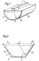
- Figure 1 represents an optimum design geometry for achieving minimum parasitic series resistance in high frequency, eg microwave diodes in particular mixer/detector diodes.
- This device comprises an elongated "stripe" rectifying contact 1 disposed axially along the flat surface of a semi-cylindrical semiconductor body 2 comprising a main high conductivity n layer 2a providing a substrate for a thin n-type active layer 2b, formed with an ohmic contact 3 over its curved surface.
- This geometry maximises the spread of current flow from the rectifying contact into the semi-conducting body.
- the parasitic series resistance for devices of this kind is composed of three contributions; the resistance of the ohmic contact; the spreading resistance within the semiconductor body 2 from the edge of the depletion region to the ohmic contact 3; and the resistance of the rectifying "stripe" contact 1 metallisation.
- Ohmic contacts are characterised by a specific contact resistetance ⁇ c , the resistance of the contact being given by - where A is the area of contact.
- the resistance contribution of the semiconductor body is a function of the radial distance r between the rectifying and ohmic contacts of the device. As the distance r is reduced bringing the ohmic contact closer to the rectifying contact to reduce the spreading distance contribution, the resistance of the ohmic contact will consequently increase as its area decreases. For a given geometry therefore there is an optimum value for the distance r, and this is given approximately as
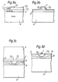
- the desired shape may conveniently be approximated by anisotropic etching to produce faceting on a suitably oriented semiconductor material as illustrated in Figure 2 for a GaAs device.
- the dotted line represents the desired semi-circular cross-section, while the actual cross-section of the device shown is produced by anisotropic etching of GaAs.
- the fabrication procedure initially comprises forming a GaAlAs buffer layer 5 between 0.5 to 2 microns thick on the surface of a semi-insulating (SI) GaAs substrate 4, typically several hundred microns thick, and forming on the surface of, the GaAlAs buffer layer 5, a layer 2 of GaAs comprising a first active n type layer 2b followed by the n + "substrate" layer 2a.
- the buffer layer 5 and the GaAs layer 2 are both formed epitaxially, eg by liquid or vapour phase, or molecular beam epitaxy.
- the thickness of the GaAs active n layer 2b will be between 0.1 and 0.3 microns and have a dopant concentration between 5x10 16 and 2x10 17 carriers/cm 3.
- the GaAs n layer 2b is formed to a thickness of 0.1 to 0.2 microns, and a lower carrier concentration of between 5x10 15 and 2x10 16 . In either case these parameters are chosen in accordance with conventional Schottky barrier and Mott diode design criteria.
- the n substrate has a thickness of about 3 microns and a carrier concentration of about 2x10 18 per cm 3 .
- the exposed regions of the GaAs layer 2 a - and underlying layer 2 b are then etched away using an orientation-selective etchant, such as a 90:5:5 mixture of H 2 O, 100V H 2 O 2 and 35% NH 4 OH.
- an orientation-selective etchant such as a 90:5:5 mixture of H 2 O, 100V H 2 O 2 and 35% NH 4 OH.
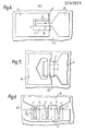
- the etch mask is then removed, and an ohmic contact 3 is formed in conventional manner overlying substantially the whole of the exposed surface of the GaAs layer 20 thus formed,apart from a small section at least at one end, and extending onto the surface of the surrounding GaAlAs buffer layer at one, or both sides as shown.
- This provides a contact pad 6 for external connection to the completed device (see Figure 4).
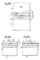
- the structure at this stage is shown in Figure 3(b).
- a support substrate 11 is applied to the surface of the structure overlying the ohmic contact.
- This support substrate 11 can be applied using any suitable low temperature technique which does not adversely affect the existing structure.
- One suitable technique used in the present example comprises the formation of an initial coating 13 of an insulating material on the surface of the structure to which the support substrate is applied using a suitable adhesive.
- One suitable insulating material for the coating 13 is polyimide; such as that sold under the name of KERIMID (Registered Trade Mark) 601 by Rhone Poulenc, a condensation type polymer resin.
- the resin which is sold in powdered form is dissolved in a solvent and applied to the surface of the existing structure which is then spun at high speed to achieve a uniform coating of the desired thickness.
- the solvent is then dried at a temperature of about 120°C before curing at a temperature of about 240°C to give a hardened coating.
- it may be built up from a number of successively applied thinner layers (typically of submicron thickness), successive layers being cured before application of the next.
- any suitable adhesive 14 may then-be used to affix the insulating support substrate 11 to the coating 13.
- an epoxy resin may be used or, as in the present embodiment a similar polyimide material as the coating 13 which may be applied as a solution and then cured to form the bond.
- the support substrate 11 may suitably comprise alumina, glass or a plastics material. The device at this stage is shown in Figure 3(c).
- the purpose of the support substrate 11 is to provide a mechanical support for the GaAs layers 2 a , 2 b and the ohmic contact 3 associated with it, so that the original semi- conductor substrate 4 can be removed together with the buffer layer 5 exposing the surface of the active GaAs layer 22. Removal of the original GaAs substrate 4 is effected using a selective etching procedure in which the GaAlAs buffer. layer 5 provides a chemical stop for the etchant used in removing the GaAs substrate 4, following which the buffer layer is removed using an etchant to which the GaAs layer 2 is resistant. In this way the free surface of the GaAs layer 2 is opposite to that on which the ohmic corttact 3 is fortned, ie thd surface of layer 2 b , is exposed for further device fabrication procedures.
- the original semi-insulating GaAs substrate 4 is removed using a 95:5 100 V 2 H 2 O 2 , 35% NH 4 OH mixture which attacks GaAs at a much faster rate than it attacks GaAlAs, about 2 orders of magnitude for an Al content of 60%, causing the etch to stop abruptly at the GaAs/GaAlAs interface.
- the GaAlAs buffer layer 5 is then removed using a different etchant, a 50% solution of HF, which attacks the GaAlAs at a faster rate than it attacks GaAs, the rate again being dependent upon the proportion of Al in the GaAlAs layer, again about 2 orders of magnitude for Ga 0.4 Al 0.6 As. Because the buffer layer 5 is relatively thin, 1 ⁇ 2 to 2 microns, and because of the high differential etch rates, its removal can be effected without affecting the uniformity of the GaAs layers 2 a , 2 b .
- a small surface thickness of the exposed n-type GaAs material 2b may optionally be removed by etching to remove surface defects and impurities.
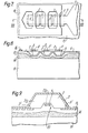
- An elongated stripe metallic electrode 1 is then formed extending axially along the centre of the exposed GaAs surface to form a metal-semiconductor junction in known manner.
- the stripe electrode 1 terminates at one end adjacent to but spaced from one edge of the exposed GaAs surface while its other end extends across the opposite edge of this surface onto the surrounding surface of the insulating coating 13 where it terminates in an enlarged contact portion 16 as shown in Figure 4.
- the rectifying stripe contact 1 is isolated from the underlying ohmic contact 3 as it traverses this edge by a small section of the GaAs material 2 which overlaps the edge of the ohmic contact 3 as described earlier, and as shown in Figure 4.
- the rectifying contact 1 is formed by evaporation of Ti/Pd/Au through a standard photolithographic mask, although any suitable alternative technique may be used.
- the dimensions and aspect ratio,ie length to width ratio,of the stripe contact 1 are important criteria in , determining the operating characteristics of the device.
- the total series resistance R T of the device 1 is the sum of three major contributions, namely the contact resistance R C between the ohmic contact 3 and the n GaAs material 2 a ; the metallisation resistance R M of the rectifying contact itself; and spreading resistance R S defined earlier.
- the value of R S can be reduced simply by increasing the length 1 of the device 1, say by a factor F, in which case the contact resistance R C will reduce by the same factor. But increasing the length of the device by a factor F will also increase the capacity of the rectifying contact by the same factor. and so to maintain a fixed capacity, for this contact, its width w must simultaneously be reduced by the same factor F.
- the capacity of the rectifying contact in mixer diodes of this kind determines the maximum operating frequency of the device, and is related to the area of the contact.
- the metallisation resistance R M of , the contact 1 can be further reduced by contacting it from both ends as shown. in Figure 5.
- the resistance R M is approximately reduced by a factor of 4 as compared with the single-end feed arrangement of Figure 4.
- the device shown in cross-section in Figure 9 illustrates one method of increasing the angle through which current spreads radially from the rectifying contact 1 to the ohmic contact 3.
- the rectifying contact 1 is recessed into the surface of the GaAs body 2, and to reduce the series resitance, an extra ohmic contact layer 3' may be applied as shown, extending onto the longitudinal edges of the flat surface of the semi-conductor body 2.
- a preferred fabrication procedure for this type of device initially comprises forming, eg by epitaxial growth, a layer 2a of high conductivity (n + ) semiconductor material on the surface of a temporary substrate (not shown) which may be the same as that used in the fabrication processed described above.
- the thickness of this high conductivity layer is slightly greater than the required radius r of the device body, ie about 3.5 ⁇ m.
- a photolithographic etching mask is then deposited on the surface of the high conductivity layer 2a having an elongated hole therein corresponding in length to the desired length of the rectifying first contact 1 of the device.
- a recess 20 is then formed in the layer 2a by anistropic etching through the mask to a depth of about 0.5 microns, and an active layer 2b is then formed in the n + material at the base of the recess 20 by ion implantation through the same mask followed by annealing.
- Tungsten metallisation for the rectifying stripe contact 1 is then deposited along the floor of the recess in contact with the active region 2b, and an ohmic contact metallisation 3' applied to the surface of the n layer 2a along both sides of the recess 20, but spaced therefrom by a distance of about 1 to 1.5 ⁇ m.
- a permanent support substrate 11 is then applied to the structure as before, using a coating 13 and an adhesive 14, and the temporary substrate (not shown) is removed to expose the other side of the n layer 2a. This is then profiled, as before, using an anistropic etching process to define a substantially cylindrical body axially aligned with the stripe contact 1.
- An ohmic contact metallisation 3 is then applied to the profiled surface of the n layer 2a extending into contact with the previously applied ohmic contact metallisation 3' on either side of the device.
- the whole device is then heated to form an ohmic contact between the ohmic contact metallisation 3,3' and the n region 2a of the device body.
- Figure 10 illustrates various stages in the fabrication of a further form of device in accordance with the present invention in which the angle through which current from the rectifying contact 1 can spread out through the GaAs body towards the ohmic contact 3, is extended to 2 ⁇ radians.
- the GaAlAs buffer layer 5 and n-type GaAs body layer 2 are epitaxially grown on the surface of a semi-insulating GaAs substrate 4 as before.
- the GaAs layer 2 consists of a high-conductivity n GaAs substrate region 2a having a thin low-doped n-type active surface region 2b formed, for example, by ion implantation as before.
- a tungsten rectifying contact metallisation is then defined, using similar procedures to those described earlier to provide the narrow stripe rectifying contact 1, contacted at one or both ends by an enlarged contact pad portion (not shown) for single or double-end feed as appropriate.
- a second layer 2' of GaAs material, equal in thickness to the first, is then grown epitaxially on the surface of the first GaAs layer 2. This involves growing an initial layer of n + GaAs having a thickness equal to the required thickness of the n type active region, selectively ion implanting the n type active region 2'b therein surrounding the stripe contact 1, and then completing the layer 2'by continued growth of n + material to a thickness equal to that of the first layer 2.
- the formation of the second GaAs layer 2 t on the surface of the first layer 2 such that the rectifying stripe contact 1 is embedded between the two layers involves a new technology developed for the fabrication of the permeable base transister described by C 0 Bozler et al in "Fabrication and Microwave performance of the Permeable Base Transistor" in the Conference Digest of IEDM, Washington DC December 1979.
- This technique shows that when GaAs is epitaxially grown on a GaAs surface formed with a thin (about 100- ⁇ ) metallisation pattern in the form of a grid of a high melting point metal, such as tungsten, which does not react with the GaAs, then as the thickness of the grown GaAs increases, the material grows between the interstices of the grid and spreads over the metallisation pattern, eventually embedding it completely.
- a similar effect is achieved when the grid is replaced by a narrow metal stripe as in the present example, and the technique results in a rectifying metal-semiconductor junction between the epitaxially grown GaAs and the embedded metallisation.
- the resulting structure is shown in Figure 10(b), and it will be appreciated that only the narrow stripe portion 1 of the contact metallisation is embedded leaving the enlarged contact pad portion, (not shown) exposed.
- the fabrication procedure then continues as in the process described with reference to Figure 3, with the orientation-selective etching of the upper GaAs layer 2' to define an approximate semi-cylindrical shape centred on the buried stripe electrode 1 which will provide one half of the GaAs body of the completed device.
- a metallisation layer 3 for the ohmic contact for this half of the device is then applied, but not annealed, as shown in Figure 10(c).
- a permanent support substrate 11, for example of alumina, is then applied to the surface of the structure which carries the ohmic metallisation 3 ( Figure 10(d)), and the temporary GaAs substrate and GaAlAs buffer layer 5 are removed by selective etching using identical procedures to those described with reference to Figure 3.
- the structure at this stage is illustrated in Figure 10 (e).
- the GaAs layers 2,2' are both grown on the (100) plane,but only one of the layers may be anisotropically etched to produce the required cross-section, the other then being defined by an isotropic etching process, eg ion milling, which will achieve the required result.
- a further layer of ohmic contact metallisation 3 is then formed as shown in Figure 10(f), and the whole structure then annealed to optimise the ohmic contacts.
- the resulting device comprises a narrow rectifying metal stripe contact 1 at the centre of a cylinder of GaAs surrounded by an ohmic contact metallisation.
- Similar design criteria to those for the semi- : cylindrical devices outlined earlier may also be applied in optimising the design of the cylindrical device.
- the parallel connection of a number of single or double end ' fed cylindrical devices, as described with reference to Figures 6 to 8 for the semi-cylindrical configurations, may also be used to minimise the series resistance as before.
- the above described process of epitaxially growing semiconductor material over the narrow stripe contact 1 may also be used to form a device of semi-cylindrical configuration.
- the metallis tion for the stripe electrode may be formed directly on the surface of a suitable semi-insulating substrate, and the semiconductor layer required for the body of the device then epitaxially grown onto this surface covering the narrow portion 1 of the contact, and forming a rectifying contact between them.
- the epitaxial layer is then profiled as before to define the required approximately semi-cylindrical body shape, followed by formation of the ohmic contact 3.
- the device configuration would then resemble that illustrated in Figure 10(c), except that the buffer layer 5 and lower semiconductor layer 2 would be omitted.
- the buffer layer may be retained, and the structure then applied to a permanent substrate followed by removal of the "temporary" semiconductor substrate 4 as before, to leave a device substantially as shown in Figure 10(e), but without the overlying semiconductor layer 2.
Landscapes
- Electrodes Of Semiconductors (AREA)
Applications Claiming Priority (2)
| Application Number | Priority Date | Filing Date | Title |
|---|---|---|---|
| GB8021448 | 1980-07-01 | ||
| GB8021448 | 1980-07-01 |
Publications (2)
| Publication Number | Publication Date |
|---|---|
| EP0043654A2 true EP0043654A2 (de) | 1982-01-13 |
| EP0043654A3 EP0043654A3 (de) | 1982-09-22 |
Family
ID=10514430
Family Applications (1)
| Application Number | Title | Priority Date | Filing Date |
|---|---|---|---|
| EP81302625A Withdrawn EP0043654A3 (de) | 1980-07-01 | 1981-06-12 | Halbleiterdioden und Verfahren zu ihrer Herstellung |
Country Status (2)
| Country | Link |
|---|---|
| EP (1) | EP0043654A3 (de) |
| JP (1) | JPS5799786A (de) |
Cited By (5)
| Publication number | Priority date | Publication date | Assignee | Title |
|---|---|---|---|---|
| RU2165661C1 (ru) * | 2000-03-27 | 2001-04-20 | Московский государственный институт стали и сплавов (технологический университет) | Выпрямительный диод шоттки (варианты) |
| RU2168800C1 (ru) * | 2000-11-28 | 2001-06-10 | Московский государственный институт стали и сплавов (технологический университет) | Лавинно-пролетный диод (варианты) |
| RU2168801C1 (ru) * | 2000-11-28 | 2001-06-10 | Московский государственный институт стали и сплавов (технологический университет) | Диод ганна (варианты) |
| RU2168799C1 (ru) * | 2000-07-07 | 2001-06-10 | Московский государственный институт стали и сплавов (технологический университет) | Полупроводниковый выпрямительный диод (варианты) |
| RU2411611C1 (ru) * | 2009-10-21 | 2011-02-10 | Юрий Робертович Гунгер | Диод силовой низкочастотный выпрямительный непланарный и способ его изготовления |
Family Cites Families (3)
| Publication number | Priority date | Publication date | Assignee | Title |
|---|---|---|---|---|
| DE889656C (de) * | 1944-02-11 | 1953-09-14 | Siemens Ag | Detektor zur Gleichrichtung elektromagnetischer Wellen, insbesondere Ultra-Kurzwellen |
| DE2324780C3 (de) * | 1973-05-16 | 1978-07-27 | Siemens Ag, 1000 Berlin Und 8000 Muenchen | Verfahren zum Herstellen eines Halbleiterbauelements |
| FR2420846A1 (fr) * | 1978-03-21 | 1979-10-19 | Thomson Csf | Structure semi-conductrice a avalanche comportant une troisieme electrode |
-
1981
- 1981-06-12 EP EP81302625A patent/EP0043654A3/de not_active Withdrawn
- 1981-07-01 JP JP56103128A patent/JPS5799786A/ja active Pending
Cited By (5)
| Publication number | Priority date | Publication date | Assignee | Title |
|---|---|---|---|---|
| RU2165661C1 (ru) * | 2000-03-27 | 2001-04-20 | Московский государственный институт стали и сплавов (технологический университет) | Выпрямительный диод шоттки (варианты) |
| RU2168799C1 (ru) * | 2000-07-07 | 2001-06-10 | Московский государственный институт стали и сплавов (технологический университет) | Полупроводниковый выпрямительный диод (варианты) |
| RU2168800C1 (ru) * | 2000-11-28 | 2001-06-10 | Московский государственный институт стали и сплавов (технологический университет) | Лавинно-пролетный диод (варианты) |
| RU2168801C1 (ru) * | 2000-11-28 | 2001-06-10 | Московский государственный институт стали и сплавов (технологический университет) | Диод ганна (варианты) |
| RU2411611C1 (ru) * | 2009-10-21 | 2011-02-10 | Юрий Робертович Гунгер | Диод силовой низкочастотный выпрямительный непланарный и способ его изготовления |
Also Published As
| Publication number | Publication date |
|---|---|
| EP0043654A3 (de) | 1982-09-22 |
| JPS5799786A (en) | 1982-06-21 |
Similar Documents
| Publication | Publication Date | Title |
|---|---|---|
| EP0518683B1 (de) | Metall-Halbleiter Feldeffekttransistor hoher Leistung und hoher Frequenz, hergestellt aus Siliziumcarbid | |
| US6329675B2 (en) | Self-aligned bipolar junction silicon carbide transistors | |
| US6218254B1 (en) | Method of fabricating a self-aligned bipolar junction transistor in silicon carbide and resulting devices | |
| US4711858A (en) | Method of fabricating a self-aligned metal-semiconductor FET having an insulator spacer | |
| US4566172A (en) | Method of fabricating a static induction type recessed junction field effect transistor | |
| US4543706A (en) | Fabrication of junction field effect transistor with filled grooves | |
| US4883767A (en) | Method of fabricating self aligned semiconductor devices | |
| US4651407A (en) | Method of fabricating a junction field effect transistor utilizing epitaxial overgrowth and vertical junction formation | |
| US6660616B2 (en) | P-i-n transit time silicon-on-insulator device | |
| US6815304B2 (en) | Silicon carbide bipolar junction transistor with overgrown base region | |
| US4611384A (en) | Method of making junction field effect transistor of static induction type | |
| US6037646A (en) | High-frequency GaAs substrate based schottky barrier diodes | |
| EP0142216B1 (de) | Verfahren zur Herstellung eines Transistors mit der Source gegenüberliegendem Gate | |
| US5098853A (en) | Self-aligned, planar heterojunction bipolar transistor and method of forming the same | |
| EP0148595A2 (de) | Verfahren zum Herstellen eines Mesa-MOSFET unter Verwendung von Überhangmasken und daraus resultierende Anordnung | |
| US4729967A (en) | Method of fabricating a junction field effect transistor | |
| EP0043654A2 (de) | Halbleiterdioden und Verfahren zu ihrer Herstellung | |
| US4459605A (en) | Vertical MESFET with guardring | |
| JP2003504855A (ja) | 金属半導体コンタクトを備えたダイオード、および金属半導体コンタクトを備えたダイオードの製造方法 | |
| US20030157777A1 (en) | Method of fabricating self-aligned silicon carbide semiconductor devices | |
| US5496743A (en) | Method of making an article comprising a semiconductor device | |
| US5066603A (en) | Method of manufacturing static induction transistors | |
| US5159423A (en) | Self-aligned, planar heterojunction bipolar transistor | |
| US5814548A (en) | Process for making n-channel or p-channel permeable base transistor with a plurality layers | |
| US5837570A (en) | Heterostructure semiconductor device and method of fabricating same |
Legal Events
| Date | Code | Title | Description |
|---|---|---|---|
| PUAI | Public reference made under article 153(3) epc to a published international application that has entered the european phase |
Free format text: ORIGINAL CODE: 0009012 |
|
| AK | Designated contracting states |
Designated state(s): DE FR GB IT NL |
|
| PUAL | Search report despatched |
Free format text: ORIGINAL CODE: 0009013 |
|
| AK | Designated contracting states |
Designated state(s): DE FR GB IT NL |
|
| STAA | Information on the status of an ep patent application or granted ep patent |
Free format text: STATUS: THE APPLICATION IS DEEMED TO BE WITHDRAWN |
|
| 18D | Application deemed to be withdrawn |
Effective date: 19830828 |
|
| RIN1 | Information on inventor provided before grant (corrected) |
Inventor name: SULLIVAN, ARTHUR BASIL JOSEPH Inventor name: VOKES, JOHN CHARLES Inventor name: DEADMAN, HARRY ALEXANDER |