EP0043224A2 - Scheinelement-Maske für gedruckte Schaltungsplatten - Google Patents
Scheinelement-Maske für gedruckte Schaltungsplatten Download PDFInfo
- Publication number
- EP0043224A2 EP0043224A2 EP81302825A EP81302825A EP0043224A2 EP 0043224 A2 EP0043224 A2 EP 0043224A2 EP 81302825 A EP81302825 A EP 81302825A EP 81302825 A EP81302825 A EP 81302825A EP 0043224 A2 EP0043224 A2 EP 0043224A2
- Authority
- EP
- European Patent Office
- Prior art keywords
- lead
- pins
- printed circuit
- holes
- circuit board
- Prior art date
- Legal status (The legal status is an assumption and is not a legal conclusion. Google has not performed a legal analysis and makes no representation as to the accuracy of the status listed.)
- Granted
Links
Images
Classifications
-
- H—ELECTRICITY
- H05—ELECTRIC TECHNIQUES NOT OTHERWISE PROVIDED FOR
- H05K—PRINTED CIRCUITS; CASINGS OR CONSTRUCTIONAL DETAILS OF ELECTRIC APPARATUS; MANUFACTURE OF ASSEMBLAGES OF ELECTRICAL COMPONENTS
- H05K3/00—Apparatus or processes for manufacturing printed circuits
- H05K3/0094—Filling or covering plated through-holes or blind plated vias, e.g. for masking or for mechanical reinforcement
-
- B—PERFORMING OPERATIONS; TRANSPORTING
- B23—MACHINE TOOLS; METAL-WORKING NOT OTHERWISE PROVIDED FOR
- B23K—SOLDERING OR UNSOLDERING; WELDING; CLADDING OR PLATING BY SOLDERING OR WELDING; CUTTING BY APPLYING HEAT LOCALLY, e.g. FLAME CUTTING; WORKING BY LASER BEAM
- B23K35/00—Rods, electrodes, materials, or media, for use in soldering, welding, or cutting
- B23K35/22—Rods, electrodes, materials, or media, for use in soldering, welding, or cutting characterised by the composition or nature of the material
- B23K35/224—Anti-weld compositions; Braze stop-off compositions
-
- H—ELECTRICITY
- H05—ELECTRIC TECHNIQUES NOT OTHERWISE PROVIDED FOR
- H05K—PRINTED CIRCUITS; CASINGS OR CONSTRUCTIONAL DETAILS OF ELECTRIC APPARATUS; MANUFACTURE OF ASSEMBLAGES OF ELECTRICAL COMPONENTS
- H05K2203/00—Indexing scheme relating to apparatus or processes for manufacturing printed circuits covered by H05K3/00
- H05K2203/05—Patterning and lithography; Masks; Details of resist
- H05K2203/0548—Masks
- H05K2203/0557—Non-printed masks
-
- H—ELECTRICITY
- H05—ELECTRIC TECHNIQUES NOT OTHERWISE PROVIDED FOR
- H05K—PRINTED CIRCUITS; CASINGS OR CONSTRUCTIONAL DETAILS OF ELECTRIC APPARATUS; MANUFACTURE OF ASSEMBLAGES OF ELECTRICAL COMPONENTS
- H05K3/00—Apparatus or processes for manufacturing printed circuits
- H05K3/30—Assembling printed circuits with electric components, e.g. with resistor
- H05K3/32—Assembling printed circuits with electric components, e.g. with resistor electrically connecting electric components or wires to printed circuits
- H05K3/34—Assembling printed circuits with electric components, e.g. with resistor electrically connecting electric components or wires to printed circuits by soldering
- H05K3/3452—Solder masks
-
- H—ELECTRICITY
- H05—ELECTRIC TECHNIQUES NOT OTHERWISE PROVIDED FOR
- H05K—PRINTED CIRCUITS; CASINGS OR CONSTRUCTIONAL DETAILS OF ELECTRIC APPARATUS; MANUFACTURE OF ASSEMBLAGES OF ELECTRICAL COMPONENTS
- H05K3/00—Apparatus or processes for manufacturing printed circuits
- H05K3/30—Assembling printed circuits with electric components, e.g. with resistor
- H05K3/32—Assembling printed circuits with electric components, e.g. with resistor electrically connecting electric components or wires to printed circuits
- H05K3/34—Assembling printed circuits with electric components, e.g. with resistor electrically connecting electric components or wires to printed circuits by soldering
- H05K3/3457—Solder materials or compositions; Methods of application thereof
- H05K3/3468—Applying molten solder
-
- Y—GENERAL TAGGING OF NEW TECHNOLOGICAL DEVELOPMENTS; GENERAL TAGGING OF CROSS-SECTIONAL TECHNOLOGIES SPANNING OVER SEVERAL SECTIONS OF THE IPC; TECHNICAL SUBJECTS COVERED BY FORMER USPC CROSS-REFERENCE ART COLLECTIONS [XRACs] AND DIGESTS
- Y10—TECHNICAL SUBJECTS COVERED BY FORMER USPC
- Y10T—TECHNICAL SUBJECTS COVERED BY FORMER US CLASSIFICATION
- Y10T29/00—Metal working
- Y10T29/49—Method of mechanical manufacture
- Y10T29/49002—Electrical device making
- Y10T29/49117—Conductor or circuit manufacturing
- Y10T29/49124—On flat or curved insulated base, e.g., printed circuit, etc.
- Y10T29/4913—Assembling to base an electrical component, e.g., capacitor, etc.
- Y10T29/49139—Assembling to base an electrical component, e.g., capacitor, etc. by inserting component lead or terminal into base aperture
Definitions
- the present invention relates to a component mask for preserving unoccupied lead-holes in a printed circuit board during mass connection of components thereto,
- a printed circuit board generally is a sheet of a rigid non-conductive material having electrically conductive lead patterns printed or otherwise provided on one or both of its sides.
- the lead patterns connect various terminal lead-holes extending through the underlying board, and the desired circuit is formed by installing electrical and electronic components, such as integrated circuit chips, transisters) etc., on the board with their terminals protruding into and through the lead-holes.
- the terminals of the components are then attached to the printed circuit board by soldering or the like to provide both physical connection of the components to the board and electrical connection of their terminals to the conductive lead patterns.
- the difficulty with use of wave soldering is that it is incapable of discriminating between those lead-holes extending through a printed circuit board which in fact have component terminals extending therethrough, and those lead-holes which do not. And it is not unusual for it to be desirable to keep unobstructed of solder at least some of those lead-holes which are unoccupied by component terminals at the time of wave soldering. For example, for some circuitry it is desirable to be able to secure some electronic components to a board after most are already secured thereto by wave soldering. Moreover, it is not unusual for component parts to be unavailble due to supply shortages and the like, at the time it is desired that a board be subjected to wave soldering.
- Toothpicks which are only loosely engaged within a hole have the disadvantage of either leaving too restricted of an unobstructed lead-hole, or falling out before or during wave soldering.
- the high temperature associated with wave soldering also chars toothpicks; leaving charred residue within the lead-holes.
- a plurality of uniformly tapered metal pins embedded in a supporting block has been used to mask lead-holes during mass soldering of printed circuit boards.
- the pins are tapered so that they wedge against the edge of the lead-holes to hold the supporting block spaced away from the printed circuit board.
- the metal pins are constructed of a material that is thermally conductive while at the same time not being susceptible to wetting by most common fluxes found in solder used in mass soldering processes. These combined characteristics of the pin material prevents solder from entering the lead-holes. However, such non-soldering metal pins are susceptible to wetting by highly active fluxes. When wetted, solder is permitted to enter the lead-holes and adhere to the pins.
- the present invention provides a component mask for preserving unoccupied lead-holes in a printed circuit board when it is subjected to a mass connection material while permitting wetting of the walls defining the lead-holes, which is simple, reliable, installable at any time prior to such mass connection, and does not leave unwanted residue either on the underneath side of the board or within the lead-holes.
- the component mask of the invention comprises a supporting block from which at least one pin'protrudes.
- the pin is constructed of a plastic material that is stable in the presence of the high temperatures commonly encountered in mass soldering processes, such material referred to herein as a high temperature resistant material.
- the pin has a cross-sectional configuration and thickness enabling the same to fit into a lead-hole extending through a printed circuit board, and a length at least generally equal to the thickness of the printed circuit board so that it will extend completely through such hole.
- a single component mask of the invention is capable of simultaneously masking a plurality of adjacent board lead-holes.
- Each of the pins is secured to the mask supporting block by a transition body that acts to space the supporting block from the printed circuit board when the pin is received within a lead-hole. This facilitates cleaning of the board after a wave soldering operation. That is, the block is raised from the board to insure it does not entrap flux residue or mask portions of the surface of the board when it is subjected to water or solvent cleaning.
- each of the pins is tapered inwardly toward its free end. As will be explained in more detail below, such a pin configuration enables lead-holes to be preserved during wave soldering, while at the same time allowing their interior walls to be wetted with solder to facilitate subsequent physical and electrical securance of a component terminal therewithin.
- Board 11 includes a rigid sheet 12 of electrically non-conductive material (for example, a resin impregnated fiberglass) having patterns of electrically conductive leads 13 on its upper and lower side surfaces 14 and 16.
- a plurality of lead-holes 17 are provided extending through such board, providing receptacles for the terminals of electronic components (two of which are schematically represented and denoted by the reference numeral 18), making up a desired electrical circuit.
- the printed circuit board acts both to physically support such components and to provide the lead connections between various component terminals necessary to complete an electrical circuit.
- the electronic circuit for which a specific printed circuit board is intended typically is produced by mounting the requisite electronic components at the appropriate locations on the board with their terminals extending through the lead-holes provided for this purpose.
- the lower (underneath) surface 16 of such a printed circuit board is then subjected to a mass connection technique, such as to solder by a wave soldering process, to simultaneously secure all of the component terminals which extend through lead-holes, both physically and electrically to such lead holes.
- a mass connection technique such as to solder by a wave soldering process
- wave soldering subjects the full lower surface of a board to solder, with the result that solder will enter into and block those lead-holes which are not at the time occupied by component terminals. It is often desirable that unoccupied lead-holes be protected during wave soldering to preserve the same for subsequent installation of components.
- the art generally has relied upon the masking at such holes with tape or a material such as latex prior to board assembly for this purpose, or the utilization of toothpicks or the like to plug such holes. The difficulties and disadvantages associated with such procedures is discussed infra.
- the present invention provides a component mask for preserving unoccupied lead-holes during soldering, having significant advantages over prior mechanisms and approaches to attempting.to preserve such unoccupied lead-holes.
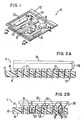
- Embodiments of such component mask are illustrated installed on board 11, at 19-24.
- Each of such components includes a supporting block 26 from which one or more pins 27 protrude.
- the pins i 27 protruding.from each supporting block are generally parallel to one another.
- each of the pins 27 has a length at least generally equal to the thickness of the printed circuit board so that it will extend completely through the lead-hole.' This is necessary to assure that solder will not plug the lower portion of such lead-holes.
- FIGS. 4A and 4B are each end views, respectively, of a single row and double row mask.
- the pins of each are spaced apart from one another by distances generally equal to distances commonly provided between lead-holes on printed circuit boards. That is, the pins in each row are placed on .100" centers, and adjacent rows are spaced .30-0" from one another.
- differing lengths of component masks providing correspondingly differing numbers of pins are provided.
- it is designed to enable such differing lengths to be provided, without a corresponding requirement on the length variations that must be provided by a manufacturer of the mask. That is, such masks are made of a material which can be easily cut or broken, and the manufacturer then need only provide relatively long embodiments of the single and double row masks.
- One manufacturer is providing a single row pin embodiment having 24 pins.
- the masks 19, 22 and 24 illustrated in FIG. 1, are formed from such an embodiment.
- the same manufacturer is providing a double row embodiment having two rows of 16 pins.
- Such embodiment illustrated in FIG. 2B is espe-.
- a suitable material for component masks of the invention is glass filled nylon, with the percentage of glass fiber being 20% to 40%.
- the component mask can be molded, and can include suitable coloring pigmentation.
- the coloring material which is included is a low-friction material, such as carbon-black, it is desirable that a significant portion of the coloring material be included to aid in lowering the coefficient of friction of the pins and thereby facilitate their insertion into board lead-holes.
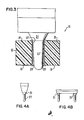
- FIG. 3 a significantly enlarged portion of a printed circuit board sheet 12 having leads 13 on each of its sides projecting into a terminal hole 17' is illustrated.
- a pin 27' of a component mask of the invention is shown extending through the lead-hole to thereby block the same.
- the pin has a cross-sectional configuration and thickness enabling the same to fit into such lead-hole.
- lead-holes are circular in cross-section and most desirably the pin has a corresponding circular cross-section.
- Most printed circuit board holes have a diameter of at least about .03", and the pins of the component masks are provided with a diameter slightly less to facilitate easy insertion into the board holes.
- the pins taper slightly inwardly toward their free end. This slight tapering is illustrated in FIG. 3. Such tapering not only facilitates insertion of the pins into the holes by reducing the dimensions of the free ends, but also results in the walls of the lead-holes themselves being wetted by solder during the wave soldering operation. That is, because each of the pins has a relatively loose fit at the underneath surface of the board by reason of such taper, solder is capable of entering into its associated lead-hole and coating its interior wall surface. Such a solder coating is represented in FIG. 3 at 29. Wetting of the lead-holes enhances the likelihood of good electrical contact with, and physical securance to, component terminals subsequently inserted into such holes. As an example of suitable tapering, pins that are approximately .1" long can be tapered approximately .003" from their base to their tip.
- the pins of each component mask should have a cross-sectional area at their base which is generally the same as the cross-sectional areas of the lead-holes for which they are designed.
- a maximum base cross-sectional area of between about .030" and .033" is generally suitable.
- different embodiments of the masks of the invention be provided, having different pin cross-sectional areas at the extremes of such range. This will enable differing sized lead-holes to be easily accommodated.
- One manufacturer of the masks of the invention is _providing single pin embodiments with the pins tapering from .030" at their bases to .027" at their tips, and double pin embodiments at which the pins taper from .033" to .030".
- transition bodies are provided for the pins to space the supporting block from the printed circuit board when :such pins are received within lead-holes.
- Such transition bodies are denoted in the figures by the reference numeral 31 and, as illustrated, are generally conical in shape. That is, each is an inverted conic section having generally the same cross-sectional dimensions at its lower end as the pin with which it is' associated. And it tapers conically outward from its connection to its associated pin, to the supporting block.
- the primary purpose of the transition bodies 31 is to space the supporting block of each mask away from the surface of the board on which such mask is mounted. This ensures that such supporting block will not entrap flux residue, and enables the board surface to be unob- structedly flushed with a cleaning fluid.
- the conical shape of the transition bodies is advantageous in this respect, in the sense that because of their large cross-section relative to the pins, they are assured of spacing the block away from the board. However, because they have generally the same cross-sectional dimensions as such pins at their point of connection thereto, they themselves do not obstruct the board surface.
- the inverted conical shape of the transition bodies assures that the upper end of each of the lead-holes receiving a pin is closed to prevent solder or the like from leaking through to the upper surface of the board.
- the masks once mounted on a board are generally self-supporting, i.e., do not require external support to remain mounted.
- a small amount of a material such as.latex can be used to adhere the single pin mask 24 to the board, for assurance that such mask will not inadvertently become separated from such board.
- component masks of the invention are to be used. Such masks simply are mounted prior to wave soldering on the side of the printed circuit board opposite that to be subjected to wave soldering, with the pins extending completely through the lead-holes to be preserved.
- One ; advantage of the instant invention is that such mounting can take place at any time prior to the wave soldering. That is, electronic components can be assembled on a board up to those components which may be missing. In the event the missing components are not available at the time wave soldering is to take place, component masks of the invention simply can be substituted therefor.
- the component mask provided on a printed circuit board can be removed simply after wave soldering by extraction with pliers or the like.
- the end and side walls of the supporting blocks of the components taper inwardly somewhat to facilitate gripping.
- one feature of the mask of the invention is that it need not be removed. That is, if it is not desired to utilize the lead-holes being preserved by a mask, the mask simply can be left in place to be a "dummy" component.
Landscapes
- Engineering & Computer Science (AREA)
- Mechanical Engineering (AREA)
- Manufacturing & Machinery (AREA)
- Microelectronics & Electronic Packaging (AREA)
- Electric Connection Of Electric Components To Printed Circuits (AREA)
Applications Claiming Priority (2)
| Application Number | Priority Date | Filing Date | Title |
|---|---|---|---|
| US163303 | 1980-06-26 | ||
| US06/163,303 US4373655A (en) | 1980-06-26 | 1980-06-26 | Component mask for printed circuit boards and method of use thereof |
Publications (3)
| Publication Number | Publication Date |
|---|---|
| EP0043224A2 true EP0043224A2 (de) | 1982-01-06 |
| EP0043224A3 EP0043224A3 (en) | 1982-10-13 |
| EP0043224B1 EP0043224B1 (de) | 1985-05-22 |
Family
ID=22589400
Family Applications (1)
| Application Number | Title | Priority Date | Filing Date |
|---|---|---|---|
| EP81302825A Expired EP0043224B1 (de) | 1980-06-26 | 1981-06-23 | Scheinelement-Maske für gedruckte Schaltungsplatten |
Country Status (3)
| Country | Link |
|---|---|
| US (1) | US4373655A (de) |
| EP (1) | EP0043224B1 (de) |
| DE (1) | DE3170586D1 (de) |
Cited By (4)
| Publication number | Priority date | Publication date | Assignee | Title |
|---|---|---|---|---|
| EP0191882A1 (de) * | 1985-02-21 | 1986-08-27 | Asahi Glass Company Ltd. | Verfahren zum Weichlöten von elektrischen Bauteilen |
| EP0298410A1 (de) * | 1987-07-06 | 1989-01-11 | Siemens Aktiengesellschaft | Elektrisches Bauteil mit Anschlussstiften |
| CN102950349A (zh) * | 2012-10-30 | 2013-03-06 | 泉州市琪祥电子科技有限公司 | 一种pcb板插件焊接工艺 |
| CN108098096A (zh) * | 2016-11-25 | 2018-06-01 | 联创汽车电子有限公司 | 选择性波峰焊排针结构及制造方法和其连锡几率判断方法 |
Families Citing this family (16)
| Publication number | Priority date | Publication date | Assignee | Title |
|---|---|---|---|---|
| US4605987A (en) * | 1983-12-22 | 1986-08-12 | Motorola, Inc. | Method of controlling printed circuit board solder fillets and printed circuit boards including solder fillet control patterns |
| US4615479A (en) * | 1985-02-21 | 1986-10-07 | Asahi Glass Company Ltd. | Method for soldering an electrical product |
| US4588468A (en) * | 1985-03-28 | 1986-05-13 | Avco Corporation | Apparatus for changing and repairing printed circuit boards |
| US4763829A (en) * | 1986-06-04 | 1988-08-16 | American Telephone And Telegraph Company, At&T Bell Laboratories | Soldering of electronic components |
| US4851966A (en) * | 1986-11-10 | 1989-07-25 | Motorola, Inc. | Method and apparatus of printed circuit board assembly with optimal placement of components |
| US4750889A (en) * | 1987-02-27 | 1988-06-14 | Minnesota Mining & Manufacturing Company | Through-board electrical component header having integral solder mask |
| US5051870A (en) * | 1990-06-11 | 1991-09-24 | Companion John A | Electronic socket attachment method and identification system |
| US5092035A (en) * | 1990-09-10 | 1992-03-03 | Codex Corporation | Method of making printed circuit board assembly |
| DE4135007C2 (de) * | 1990-10-25 | 1994-12-22 | Cts Corp | SMD-Bauelemente mit Maßnahmen gegen Lötbrückenbildung und Temperaturwechselbeanspruchung |
| US5152702A (en) * | 1991-07-05 | 1992-10-06 | Minnesota Mining Manufacturing Company | Through board connector having a removable solder mask |
| JP3093476B2 (ja) * | 1992-08-31 | 2000-10-03 | ローム株式会社 | 電子部品およびその実装方法 |
| US6651869B2 (en) | 2001-09-21 | 2003-11-25 | Intel Corporation | Methods and electronic board products utilizing endothermic material for filling vias to absorb heat during wave soldering |
| JP2009164173A (ja) * | 2007-12-28 | 2009-07-23 | Fujitsu Ltd | 基板ユニットおよびその製造方法 |
| DE102008022186B3 (de) * | 2008-05-05 | 2009-10-29 | Reel To Reel Produktionssysteme Gmbh | Verfahren zum Herstellen einer Lötstelle |
| TWI547216B (zh) * | 2012-11-23 | 2016-08-21 | Flexible circuit board and connector welding structure | |
| CN103607854A (zh) * | 2013-10-22 | 2014-02-26 | 徐州市恒源电器有限公司 | 一种结合平行移栽机和自动循环线的流水线 |
Citations (3)
| Publication number | Priority date | Publication date | Assignee | Title |
|---|---|---|---|---|
| US2916805A (en) * | 1955-08-09 | 1959-12-15 | Philco Corp | Method of securing electrical connections to printed wiring panels |
| US3576669A (en) * | 1968-08-15 | 1971-04-27 | Nasa | Method for coating through-holes |
| FR2471725A1 (fr) * | 1979-12-12 | 1981-06-19 | Philips Ind Commerciale | Technique d'isolement des trous metallises dans des cartes de circuits imprimes |
Family Cites Families (7)
| Publication number | Priority date | Publication date | Assignee | Title |
|---|---|---|---|---|
| CA602704A (en) * | 1960-08-02 | Ferranti Electric Limited | Automatic soldering development | |
| US3059152A (en) * | 1959-02-05 | 1962-10-16 | Globe Union Inc | Plug-in electronic circuit units and mounting panels |
| US3246386A (en) * | 1962-01-26 | 1966-04-19 | Corning Glass Works | Electrical connected component and method |
| US3525143A (en) * | 1967-03-24 | 1970-08-25 | Conalco Metals Inc | Method of dip soldering electrical tube sockets |
| US3524960A (en) * | 1968-11-04 | 1970-08-18 | Richardson Co | Metal coated plastic plug as electrical connector and switch |
| US3604836A (en) * | 1969-09-08 | 1971-09-14 | Sprague Electric Co | Dip-coated electrical components |
| DE2812768B2 (de) * | 1978-03-23 | 1980-09-25 | Stettner & Co, 8560 Lauf | Elektrisches Bauelement mit Anschlußdrahten zum Einstecken in Bohrungen der Platte einer gedruckten Schaltung |
-
1980
- 1980-06-26 US US06/163,303 patent/US4373655A/en not_active Expired - Lifetime
-
1981
- 1981-06-23 DE DE8181302825T patent/DE3170586D1/de not_active Expired
- 1981-06-23 EP EP81302825A patent/EP0043224B1/de not_active Expired
Patent Citations (3)
| Publication number | Priority date | Publication date | Assignee | Title |
|---|---|---|---|---|
| US2916805A (en) * | 1955-08-09 | 1959-12-15 | Philco Corp | Method of securing electrical connections to printed wiring panels |
| US3576669A (en) * | 1968-08-15 | 1971-04-27 | Nasa | Method for coating through-holes |
| FR2471725A1 (fr) * | 1979-12-12 | 1981-06-19 | Philips Ind Commerciale | Technique d'isolement des trous metallises dans des cartes de circuits imprimes |
Cited By (5)
| Publication number | Priority date | Publication date | Assignee | Title |
|---|---|---|---|---|
| EP0191882A1 (de) * | 1985-02-21 | 1986-08-27 | Asahi Glass Company Ltd. | Verfahren zum Weichlöten von elektrischen Bauteilen |
| EP0298410A1 (de) * | 1987-07-06 | 1989-01-11 | Siemens Aktiengesellschaft | Elektrisches Bauteil mit Anschlussstiften |
| CN102950349A (zh) * | 2012-10-30 | 2013-03-06 | 泉州市琪祥电子科技有限公司 | 一种pcb板插件焊接工艺 |
| CN108098096A (zh) * | 2016-11-25 | 2018-06-01 | 联创汽车电子有限公司 | 选择性波峰焊排针结构及制造方法和其连锡几率判断方法 |
| CN108098096B (zh) * | 2016-11-25 | 2020-02-25 | 联创汽车电子有限公司 | 选择性波峰焊排针结构及制造方法和其连锡几率判断方法 |
Also Published As
| Publication number | Publication date |
|---|---|
| US4373655A (en) | 1983-02-15 |
| DE3170586D1 (en) | 1985-06-27 |
| EP0043224A3 (en) | 1982-10-13 |
| EP0043224B1 (de) | 1985-05-22 |
Similar Documents
| Publication | Publication Date | Title |
|---|---|---|
| EP0043224B1 (de) | Scheinelement-Maske für gedruckte Schaltungsplatten | |
| US4442938A (en) | Socket terminal positioning method and construction | |
| US5418471A (en) | Adapter which emulates ball grid array packages | |
| US7458828B2 (en) | Electrical connector and method of producing same | |
| US5140745A (en) | Method for forming traces on side edges of printed circuit boards and devices formed thereby | |
| US4678250A (en) | Multi-pin electrical header | |
| USRE32540E (en) | Terminal positioning method and construction | |
| US4080026A (en) | Multi-level socket for an integrated circuit | |
| US3951494A (en) | Electrical connector | |
| EP0668636B1 (de) | Leiterplatte mit elektrischem Adaptorstift und dessen Herstellungsverfahren. | |
| EP0280508B1 (de) | Endstück eines eine Platte durchdringenden, elektrischen Bauelementes mit eingebauter Lötmaske | |
| EP0260967B1 (de) | Steckverbinder mit verformbarem Haltebügel | |
| USRE36442E (en) | Adapter which emulates ball grid array packages | |
| JPH05502341A (ja) | 部分のウェーブソルダリングおよび圧入に適応するプリント回路基板の製造方法 | |
| US5709555A (en) | High density card edge connection system with outrigger and sequentially connected contacts | |
| JPH0247071B2 (de) | ||
| US4932876A (en) | Adapter for removable circuit board components | |
| GB2242579A (en) | Electrical connectors for flat insulated boards | |
| US4977668A (en) | Method of making socket connector | |
| US7086870B1 (en) | Electrical connector (receptacle) with easily removable bottom | |
| US4859191A (en) | Multi-piece connector assembly | |
| JPS62150675A (ja) | ピンヘツダ− | |
| JPH0542632Y2 (de) | ||
| JPH0268982A (ja) | プリント板の実装構造 | |
| JPS63268285A (ja) | 面実装部品 |
Legal Events
| Date | Code | Title | Description |
|---|---|---|---|
| PUAI | Public reference made under article 153(3) epc to a published international application that has entered the european phase |
Free format text: ORIGINAL CODE: 0009012 |
|
| AK | Designated contracting states |
Designated state(s): CH DE FR GB |
|
| RBV | Designated contracting states (corrected) |
Designated state(s): CH DE FR GB LI |
|
| PUAL | Search report despatched |
Free format text: ORIGINAL CODE: 0009013 |
|
| AK | Designated contracting states |
Designated state(s): CH DE FR GB |
|
| 17P | Request for examination filed |
Effective date: 19830331 |
|
| GRAA | (expected) grant |
Free format text: ORIGINAL CODE: 0009210 |
|
| AK | Designated contracting states |
Designated state(s): CH DE FR GB LI |
|
| REF | Corresponds to: |
Ref document number: 3170586 Country of ref document: DE Date of ref document: 19850627 |
|
| ET | Fr: translation filed | ||
| PLBE | No opposition filed within time limit |
Free format text: ORIGINAL CODE: 0009261 |
|
| STAA | Information on the status of an ep patent application or granted ep patent |
Free format text: STATUS: NO OPPOSITION FILED WITHIN TIME LIMIT |
|
| 26N | No opposition filed | ||
| PGFP | Annual fee paid to national office [announced via postgrant information from national office to epo] |
Ref country code: FR Payment date: 19920605 Year of fee payment: 12 |
|
| PGFP | Annual fee paid to national office [announced via postgrant information from national office to epo] |
Ref country code: CH Payment date: 19920626 Year of fee payment: 12 |
|
| PG25 | Lapsed in a contracting state [announced via postgrant information from national office to epo] |
Ref country code: LI Effective date: 19930630 Ref country code: CH Effective date: 19930630 |
|
| PG25 | Lapsed in a contracting state [announced via postgrant information from national office to epo] |
Ref country code: FR Effective date: 19940228 |
|
| REG | Reference to a national code |
Ref country code: CH Ref legal event code: PL |
|
| REG | Reference to a national code |
Ref country code: FR Ref legal event code: ST |
|
| PGFP | Annual fee paid to national office [announced via postgrant information from national office to epo] |
Ref country code: DE Payment date: 19970630 Year of fee payment: 17 |
|
| PG25 | Lapsed in a contracting state [announced via postgrant information from national office to epo] |
Ref country code: DE Free format text: LAPSE BECAUSE OF NON-PAYMENT OF DUE FEES Effective date: 19990401 |
|
| PGFP | Annual fee paid to national office [announced via postgrant information from national office to epo] |
Ref country code: GB Payment date: 20000502 Year of fee payment: 20 |
|
| PG25 | Lapsed in a contracting state [announced via postgrant information from national office to epo] |
Ref country code: GB Free format text: LAPSE BECAUSE OF EXPIRATION OF PROTECTION Effective date: 20010622 |
|
| REG | Reference to a national code |
Ref country code: GB Ref legal event code: PE20 Effective date: 20010622 |