EP0039943A1 - Thyristor having controllable emitter shorts and process for its operation - Google Patents
Thyristor having controllable emitter shorts and process for its operation Download PDFInfo
- Publication number
- EP0039943A1 EP0039943A1 EP81103603A EP81103603A EP0039943A1 EP 0039943 A1 EP0039943 A1 EP 0039943A1 EP 81103603 A EP81103603 A EP 81103603A EP 81103603 A EP81103603 A EP 81103603A EP 0039943 A1 EP0039943 A1 EP 0039943A1
- Authority
- EP
- European Patent Office
- Prior art keywords
- emitter
- thyristor
- emitter layer
- layer
- cathode
- Prior art date
- Legal status (The legal status is an assumption and is not a legal conclusion. Google has not performed a legal analysis and makes no representation as to the accuracy of the status listed.)
- Granted
Links
- 238000000034 method Methods 0.000 title claims description 13
- 238000000576 coating method Methods 0.000 claims abstract description 6
- 239000004065 semiconductor Substances 0.000 claims description 14
- 230000000903 blocking effect Effects 0.000 description 2
- 239000011248 coating agent Substances 0.000 description 2
- 229910004298 SiO 2 Inorganic materials 0.000 description 1
- 230000003213 activating effect Effects 0.000 description 1
- 238000010276 construction Methods 0.000 description 1
- 238000011161 development Methods 0.000 description 1
- 230000018109 developmental process Effects 0.000 description 1
- 239000002184 metal Substances 0.000 description 1
- 229910021420 polycrystalline silicon Inorganic materials 0.000 description 1
- 229910052710 silicon Inorganic materials 0.000 description 1
- 239000010703 silicon Substances 0.000 description 1
Images

Classifications
-
- H—ELECTRICITY
- H01—ELECTRIC ELEMENTS
- H01L—SEMICONDUCTOR DEVICES NOT COVERED BY CLASS H10
- H01L29/00—Semiconductor devices adapted for rectifying, amplifying, oscillating or switching, or capacitors or resistors with at least one potential-jump barrier or surface barrier, e.g. PN junction depletion layer or carrier concentration layer; Details of semiconductor bodies or of electrodes thereof ; Multistep manufacturing processes therefor
- H01L29/66—Types of semiconductor device ; Multistep manufacturing processes therefor
- H01L29/68—Types of semiconductor device ; Multistep manufacturing processes therefor controllable by only the electric current supplied, or only the electric potential applied, to an electrode which does not carry the current to be rectified, amplified or switched
- H01L29/70—Bipolar devices
- H01L29/74—Thyristor-type devices, e.g. having four-zone regenerative action
- H01L29/744—Gate-turn-off devices
- H01L29/745—Gate-turn-off devices with turn-off by field effect
- H01L29/7455—Gate-turn-off devices with turn-off by field effect produced by an insulated gate structure
-
- H—ELECTRICITY
- H01—ELECTRIC ELEMENTS
- H01L—SEMICONDUCTOR DEVICES NOT COVERED BY CLASS H10
- H01L29/00—Semiconductor devices adapted for rectifying, amplifying, oscillating or switching, or capacitors or resistors with at least one potential-jump barrier or surface barrier, e.g. PN junction depletion layer or carrier concentration layer; Details of semiconductor bodies or of electrodes thereof ; Multistep manufacturing processes therefor
- H01L29/40—Electrodes ; Multistep manufacturing processes therefor
- H01L29/41—Electrodes ; Multistep manufacturing processes therefor characterised by their shape, relative sizes or dispositions
- H01L29/423—Electrodes ; Multistep manufacturing processes therefor characterised by their shape, relative sizes or dispositions not carrying the current to be rectified, amplified or switched
- H01L29/42308—Gate electrodes for thyristors
-
- H—ELECTRICITY
- H01—ELECTRIC ELEMENTS
- H01L—SEMICONDUCTOR DEVICES NOT COVERED BY CLASS H10
- H01L29/00—Semiconductor devices adapted for rectifying, amplifying, oscillating or switching, or capacitors or resistors with at least one potential-jump barrier or surface barrier, e.g. PN junction depletion layer or carrier concentration layer; Details of semiconductor bodies or of electrodes thereof ; Multistep manufacturing processes therefor
- H01L29/66—Types of semiconductor device ; Multistep manufacturing processes therefor
- H01L29/68—Types of semiconductor device ; Multistep manufacturing processes therefor controllable by only the electric current supplied, or only the electric potential applied, to an electrode which does not carry the current to be rectified, amplified or switched
- H01L29/70—Bipolar devices
- H01L29/74—Thyristor-type devices, e.g. having four-zone regenerative action
- H01L29/7404—Thyristor-type devices, e.g. having four-zone regenerative action structurally associated with at least one other device
- H01L29/742—Thyristor-type devices, e.g. having four-zone regenerative action structurally associated with at least one other device the device being a field effect transistor
Definitions
- the invention relates to a thyristor with controllable emitter short circuits according to the preamble of claim 1 and to a method for its operation.
- Thyristors of this type are described in German patent applications P 29 45 366.5 and P 29 45 324.5. If the controllable emitter short-circuits are designed as MIS structures of the depletion type, they each short-circuit a short-circuit path without supplying a control voltage to the gate electrodes, which bridge the PN junction between the emitter layer connected to the cathode (anode) and the adjacent base layer.
- the thyristor thus has good stability, ie a high level of security against unintended ignition processes when voltages polarized in the forward direction occur on the anode-cathode path, which in some cases rise very quickly (high dU / dt load).
- an ignition voltage pulse that can be picked up at the ignition electrode can be applied to the gate electrodes of the controllable emitter short-circuits, so that they are deactivated for the duration of the ignition.
- the ineffective circuit represents a switch-on measure and has the consequence that a quick controlled ignition takes place over the entire thyristor cross section.
- controllable emitter short-circuits are designed as MIS structures of the enhancement type, they are ineffective without supplying a control voltage to their gate electrodes and are only activated by a control voltage pulse which has the opposite PoSt 1 Ka / 2.5.1980 has larity to said Zündspannuhgsimpuls, activated for the duration of the control voltage pulse.
- Such control takes place in the current-carrying state of the thyristor for the purpose of achieving rapid blocking of the thyristor, and therefore represents a shutdown measure.
- the invention is based, to simplify the structure of a thyristor provided with controllable emitter short circuits of the type mentioned in the task substantially. This object is achieved by the features stated in claim 1.
- the advantage that can be achieved with the invention is in particular that the ignition electrode and the gate electrodes of the controllable emitter short-circuits consist of one and the same conductive coating, the edge zones of which are insulated from the interface of the semiconductor body, while another part of the coating contacts the interface.
- the conductive assignment is provided with a connection which represents both the connection for the ignition electrode and the control voltage connection for the gate electrodes of the MIS structures.
- Claims 2 to 8 are directed to preferred refinements and developments of the invention.
- Claim 9 specifies an advantageous method for operating a thyristor according to the invention.
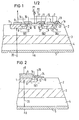
- the thyristor shown in cross section in FIG. 1 has a semiconductor body with adjoining layers 1 to 4 of alternating conductivity types, which consist, for example, of doped silicon.
- the outer N-type layer 1 is referred to as the N-emitter layer and the outer P-type layer 4 as the P-emitter layer.
- the so-called base layers adjoin each of these, namely the P base layer 2 to the N emitter layer 1 and the N base layer 3 to the P emitter layer 4.
- the P emitter layer 4 is provided with an anode 5 which has an anode connection -luß A has, while the N-emitter layer 1 is divided into two laterally adjacent N-emitter zones. Each of these emitter zones is provided with a part 6, 7 of a cathode, the individual parts of the cathode being conductively connected to one another and being guided to a common cathode connection K.
- P-type semiconductor regions 8 and 9 are inserted into the N-emitter zone 1 in such a way that they extend to the interface 1a of the semiconductor body and are contacted by the parts 6, 7 of the cathode at the edge thereof.
- 10 and 11 denote individual zones of the P base layer 2, which start from the interface 1a and laterally adjoin those parts of the N emitter zones which contain the semiconductor regions 8 and 9, respectively.
- the part 12 of the left N emitter zone 1 represents an N intermediate layer, which separates the P-type semiconductor region 8 and the P-type zone 10 from one another.
- the part 13 of the right-hand N-emitter zone 1 forms an N-intermediate layer between the parts 9 and 11.
- Thin, electrically insulating layers 14 and 15 are provided on the interface 1 a, for example made of SiO 2 , an area 16 between them free the interface 1a.
- the conductive assignment 17 has a connection which is designated ZG.
- the parts 8, 10, 12, 14 together with the left edge zone of the conductive assignment 17 form a first MIS structure
- the parts 9, 11, 13, 15 together with the right edge zone of the assignment 17 form a second MIS structure.
- the edge zones of the assignment 17 represent the gate electrodes of these structures
- the middle part of the assignment contacting the P-base layer 2 represents the ignition electrode of the thyristor.
- HIS structures are of the enhancement type, there are no inversion channels 15, 16 without supplying a voltage to the connection ZG. These are then only built up by applying a voltage which exceeds the threshold voltage and is negative with respect to the cathode connection K to ZG.
- the P-type inversion channel 18 thus represents the switching path of a controllable short circuit SK1 which, depending on a control voltage supplied to the connection ZG, connects the P-base layer 2 to the region 8 and thus to the part 6 of the cathode with low resistance or not.
- the inversion channel 19 forms the switching path of a controllable 3mitter short circuit SK2, which is connected to the terminal ZG as a function of one led control voltage optionally connects the P base layer 2 with the part 7 of the cathode.
- the emitter short-circuits SK1 and SK2 are only deactivated for the duration of the ignition process and are always active before and after the same.
- the MIS structures 8, 10, 12, 14, 17 and 9, 11, 13, 15, 17 can advantageously belong to the depletion type.
- the short circuits SK1 and SK2 are then initially effective without supplying a voltage to the connection ZG and stabilize the thyristor against high dU / dt loads which occur in the blocked state.
- the emitter short-circuits are rendered ineffective SK1 and SK2 for the duration of P1, so that each ignition area spreads in a lateral direction rapidly over the entire cross section of the thyristor .
- a load current of a load circuit connected to A and K then flows via the low-resistance switched thyristor. The same is switched off by switching off the voltage present between A and K in the forward direction, or, if it is an AC voltage, by the next zero crossing.
- the terminal ZG is in the blocked state of the thyristor at a negative bias, under the influence of which the inversion channels 18, 19 are built up.
- the negative bias voltage of ZG is then switched off and a positive ignition pulse P1 is supplied.
- the Inversion channels 18, 19 interrupted during the ignition process.
- the emitter short-circuits SK1 and SK2 are only activated and switched on when the thyristor is switched off - as a result of which it goes from the current-carrying state into the blocked state without the forward voltage at the connections A and K being switched off or always ineffective after this switch-off process.
- the MIS structures are of the enhancement type, the ignition is effected by the positive ignition pulse P1, but the blocking of the emitter short circuits SK1 and SK2 is not canceled. Only when the terminal ZG is supplied with a negative pulse P2 is the thyristor switched off by activating SK1 and SK2.
- the one MIS structure for. B. the structure 8, 10, 12, 14, 17, the depletion type and the other MIS structure, e.g. B. the structure 9, 11, 13, 15, 17 belongs to the enrichment type.
- the emitter short circuit SK1 is only when the positive ignition pulse P1 occurs, i. H. during the ignition process, deactivated and always active before or after the same, while SK2 only when a negative pulse P2 is applied, i. H. is switched off while the thyristor is switched off and is otherwise always inactive.
- SK1 serves as a switch-on aid
- SK2 represents a switch-off aid.
- a P-type semiconductor region 21 can also be provided on the right edge of the right emitter zone 1.
- the one with its left part ver with ZG forms bound gate electrode, it represents an additional controllable emitter short-circuit SKz, which according to the first and second embodiment is designed and operated in each case as SK1 and SK2.
- the MIS structure 21, 22, 23 advantageously belongs to the depletion type, so that SKz is only activated when the thyristor is switched off.
- the right part of the conductive assignment 23 contacts the P base layer 2 and represents a further part of the ignition electrode.
- the N emitter zones 1 can be elongated in FIG. 1, so that they have substantially larger dimensions perpendicular to the image plane than in the same. They then expediently run in a straight line and parallel to one another over the entire interface 1a of the thyristor, which is generally designed as a round disk.
- Line 20 can be understood as a plane of symmetry that is perpendicular to the image plane.
- the cathode part of the N-emitter zone provided on the left side of line 20 is then also connected to connection K, while the associated conductive assignments are connected to connection ZG.
- the thyristor according to FIG. 1 can also be constructed to be rotationally symmetrical, the line 20 representing the axis of symmetry. In this case, the part 6 of the cathode and the left emitter zone 1 each have a circular outline, while the parts 7, 17 and 23 and the right emitter zone 1 are ring-shaped.
- FIG. 2 shows an embodiment which is simplified compared to FIG. 1, in which the N emitter layer consists only of one emitter zone 1.
- the right part of the assignment 24 contacts the P base layer 2 and forms the ignition electrode.
- the connection of 24 is designated ZG in accordance with FIG. 1.
- the parts 1, 6 and 24 can again be elongated, in such a way that they have substantially larger dimensions perpendicular to the image plane of Figure 2 than in the same.
- the line 20 can again be understood as a plane of symmetry standing perpendicular to the image plane, in which case the conductive assignment corresponding to the part 24 and to the left of the line 20 is connected to the connection ZG.
- a rotationally symmetrical construction of the thyristor according to FIG. 2 with line 20 as an axis of symmetry is also expedient.
- SK1 can either be deactivated during the switch-on process or switched effective during the switch-off process.
- the controllable emitter short circuit to the left of it can belong to the enhancement type, the one to the right to the depletion type.
- the exemplary embodiment shown in FIG. 3 differs from FIG. 1 in that three N emitter zones 1 'to 1 "' are shown, zone 1"'being occupied by a part 7' of the cathode which is connected to the connection K. .
- a conductive covering 17' At the edge of the N-emitter zones 1 "and 1"'there is a conductive covering 17', the edge zones of which are insulated from the interface 1a and form the gate electrodes for two further controllable emitter short-circuits SK3 and SK4, while their central zone represents a further part of the ignition electrode.
- the assignment 17 ' is connected to the assignment, 17 and thus also to the connection ZG.
- the N emitter zones 1 'to 1''' can either be elongated, with the line 20 'being understood as a plane of symmetry, or a rotationally symmetrical structure of the thyristor is provided, with the line 20' as an axis of symmetry .
- the individual emitter short-circuits SK1 to SK4 can again be designed in such a way that they are either deactivated during the ignition process and are otherwise effective or that they are only effective during the switching off and are otherwise deactivated. If one divides the emitter short circuits into a first group of ones that are only inactive during the ignition process and into a second group of ones that are only activated during the switch-off, it is expedient to make the second group larger than the first. For example, the emitter short circuits SK2 to SK4 belong to the second group, while the short circuit SK1 is assigned to the first group.
- a further controllable emitter short-circuit SKz ' which is constructed in accordance with SKz in FIG.
- SKz ' is assigned to the second group, for example.
- FIG. 4 shows a plan view of a thyristor designed according to FIG. 3 with a rotationally symmetrical structure.
- the lateral boundaries of the individual N emitter zones 1 ′, 1 ′′ and 1 ′′ ′′ are shown in dashed lines, provided that they are below the conductive assignments 17, 17 ′ and 17 ′′.
- the parts 6, 7 and 7 'of the cathode are shown hatched for clarity.
- the outer edge of the upper boundary surface of the thyristor is indicated by 25, the outer edge of the P-emitter layer 4 by 26.
- the annular coatings 17 and 17 ' are connected to one another by a connecting part 27, the coatings 17' and 17 "by a connecting part 28 , the assignment 17 "being provided with the connection ZG.
- the cathode parts 6, 7 and 7 ' are expediently contacted by a cathode plate 30 (FIG. 3), the cathode connection K being attached to the cathode plate.
- the P-emitter layer 4 can also be divided into individual zones which are covered with individual, interconnected parts of the anode. Controllable P-emitter short-circuits are provided here. Figures 1 to 3 can be used to illustrate this variant if the designations of the connections A and K are interchanged and the semiconductor parts 1 to 4, 8, 9 and 21 each have the opposite conductivities to those described so far. Pulse P1 then has a negative sign, pulse P2 has a positive sign.
Abstract
Bei einem Thyristor mit gategesteuerten als MIS-Strukturen ausgebildete Emitterkurzschlüssen sind neben der N-Emitterschicht (1) eine oder mehrere leitende Belegungen (17) angeordnet, die mit ihren gegen die Emitterschicht (1) isolierten Randzonen die Gateelektroden der MIS-Strukturen (8, 10, 12, 14, 17; 9, 11, 13, 15, 17) bilden, während ihre die P-Basisschicht (2) kontaktierenden Teile die Zündelektrode darstellen.In a thyristor with gate-controlled emitter short circuits designed as MIS structures, one or more conductive coatings (17) are arranged next to the N emitter layer (1), which, with their edge zones isolated from the emitter layer (1), the gate electrodes of the MIS structures (8, 10, 12, 14, 17; 9, 11, 13, 15, 17) form, while their parts contacting the P base layer (2) constitute the ignition electrode.
Description
Die Erfindung bezieht sich auf einen Thyristor mit steuerbaren Emitterkurzschlüssen nach dem Oberbegriff des Anspruchs 1 und auf ein Verfahren zu seinem Betrieb.The invention relates to a thyristor with controllable emitter short circuits according to the preamble of
Thyristoren dieser Art sind in den deutschen Patentanmeldungen P 29 45 366.5 und P 29 45 324.5 beschrieben. Sind die steuerbaren Emitterkurzschlüsse als MIS-Strukturen des Verarmungstyps ausgebildet, so schließen sie ohne Zuführung einer Steuerspannung an ihre Gateelektroden jeweils einen Kurzschlußpfad, der den PN-Übergang zwischen der mit der Kathode (Anode) verbundenen Emitterschicht und der angrenzenden Basisschicht überbrückt. Damit weist der Thyristor eine gute Stabilität auf, d. h. eine große Sicherheit gegen unbeabsichtigte Zündvorgänge beim Auftreten von in Durchlaßrichtung gepolten Spannungen an der Anoden- Kathoden-Strecke, die teilweise sehr schnell ansteigen (hohe dU/dt-Belastung). Wird der Thyristor durch einen seiner Zündelektrode zugeführten Stromimpuls gezündet, so kann ein an der Zündelektrode abgreifbarer Zündspannungsimpuls an die Gateelektroden der steuerbaren Emitterkurzschlüsse gelegt werden, so daß diese für die Dauer der Zündung unwirksam geschaltet werden. Die Unwirksamschaltung stellt eine Einschaltmaßnahme dar und hat zur Folge, daß eine schnelle kontrollierte Zündung über dem gesamten Thyristorquerschnitt erfolgt. Falls andererseits steuerbare Emitterkurzschlüsse als MIS-Strukturen des Anreicherungstyps ausgebildet sind, so sind diese ohne Zuführung einer Steuerspannung an ihre Gateelektroden unwirksam und werden erst durch einen Steuerspannungsimpuls, der die entgegengesetzte PoSt 1 Kä / 2.5.1980 larität zu dem genannten Zündspannuhgsimpuls aufweist, für die Dauer des Steuerspannungsimpulses wirksam geschaltet. Eine solche Steuerung erfolgt im stromführenden Zustand des Thyristors zu dem Zweck, eine schnelle Blokkierung desselben zu erreichen, stellt also eine Abschaltmaßnahme dar.Thyristors of this type are described in German patent applications P 29 45 366.5 and P 29 45 324.5. If the controllable emitter short-circuits are designed as MIS structures of the depletion type, they each short-circuit a short-circuit path without supplying a control voltage to the gate electrodes, which bridge the PN junction between the emitter layer connected to the cathode (anode) and the adjacent base layer. The thyristor thus has good stability, ie a high level of security against unintended ignition processes when voltages polarized in the forward direction occur on the anode-cathode path, which in some cases rise very quickly (high dU / dt load). If the thyristor is ignited by a current pulse supplied to its ignition electrode, an ignition voltage pulse that can be picked up at the ignition electrode can be applied to the gate electrodes of the controllable emitter short-circuits, so that they are deactivated for the duration of the ignition. The ineffective circuit represents a switch-on measure and has the consequence that a quick controlled ignition takes place over the entire thyristor cross section. If, on the other hand, controllable emitter short-circuits are designed as MIS structures of the enhancement type, they are ineffective without supplying a control voltage to their gate electrodes and are only activated by a control voltage pulse which has the
Der Erfindung liegt die Aufgabe zugrunde, einen mit steuerbaren Emitterkurzschlüssen versehenen Thyristor der eingangs genannten Art in seiner Struktur wesentlich zu vereinfachen. Diese Aufgabe wird durch die im Anspruch 1 angeführten Merkmale gelöst.The invention is based, to simplify the structure of a thyristor provided with controllable emitter short circuits of the type mentioned in the task substantially. This object is achieved by the features stated in
Der mit der Erfindung erzielbare Vorteil besteht insbesondere darin, daß die Zündelektrode und die Gateelektroden der steuerbaren Emitterkurzschlüsse aus ein und derselben leitenden Belegung bestehen, deren Randzonen gegenüber'der Grenzfläche des Halbleiterkörpers isoliert sind, während ein anderer Teil der Belegung die Grenzfläche kontaktiert. Die leitende Belegung ist mit einem Anschluß versehen, der sowohl den Anschluß für die Zündelektrode darstellt als auch den Steuerspannungsanschluß für die Gateelektroden der MIS-Strukturen.The advantage that can be achieved with the invention is in particular that the ignition electrode and the gate electrodes of the controllable emitter short-circuits consist of one and the same conductive coating, the edge zones of which are insulated from the interface of the semiconductor body, while another part of the coating contacts the interface. The conductive assignment is provided with a connection which represents both the connection for the ignition electrode and the control voltage connection for the gate electrodes of the MIS structures.
Die Ansprüche 2 bis 8 sind auf bevorzugte Ausgestaltungen und Weiterbildungen der Erfindung gerichtet. Der Anspruch 9 gibt ein vorteilhaftes Verfahren zum Betrieb eines erfindungsgemäßen Thyristors an.
Die Erfindung wird nachfolgend anhand der Zeichnung näher erläutert. Dabei zeigt:
Figur 1 ein erstes Ausführungsbeispiel der Erfindung,Figur 2 ein zweites Ausführungsbeispiel,Figur 3 ein drittes Ausführungsbeispiel undFigur 4 eine Draufsicht auf das Ausführungsbeispiel nachFigur 3.
- FIG. 1 shows a first exemplary embodiment of the invention,
- FIG. 2 shows a second exemplary embodiment,
- Figure 3 shows a third embodiment and
- FIG. 4 shows a top view of the exemplary embodiment according to FIG. 3.
Der in Figur 1 im Querschnitt dargestellte Thyristor weist einen Halbleiterkörper mit aneinandergrenzenden Schichten 1 bis 4 abwechselnder Leitfähigkeitstypen auf, die beispielsweise aus dotiertem Silizium bestehen. Dabei werden die außenliegende N-leitende Schicht 1 als N-Emitterschicht und die außenliegende P-leitende Schicht 4 als P-Emitterschicht bezeichnet. An diese grenzen jeweils die sogenannten Basisschichten an, und zwar die P-Basisschicht 2 an die N-Emitterschicht 1 und die N-Basisschicht 3 an die P-Emitterschicht 4. Die P-Emitterschicht 4 ist mit einer Anode 5 versehen, die einen Anodenansch-luß A besitzt, während die N-Emitterschicht 1 in zwei lateral nebeneinanderliegende N-Emitterzonen aufgeteilt ist. Jede dieser Emitterzonen ist mit einem Teil 6, 7 einer Kathode versehen, wobei die einzelnen Teile der Kathode untereinander leitend verbunden und an einen gemeinsamen Kathodenanschluß K geführt sind.The thyristor shown in cross section in FIG. 1 has a semiconductor body with
In die N-Emitterzone 1 sind P-leitende Halbleitergebiete 8 und 9 so eingefügt, daß sie sich bis zur Grenzfläche 1a des Halbleiterkörpers erstrecken und in dieser randseitig von den Teilen 6, 7 der Kathode kontaktiert werden. Mit 10 und 11 sind einzelne Zonen der P-Basisschicht 2 bezeichnet, die von der Grenzfläche 1a ausgehen und an diejenigen Teile der N-Emitterzonen, die die Halbleitergebiete 8 bzw. 9 enthalten, lateral angrenzen. Der Teil 12 der linken N-Emitterzone 1 stellt eine N-Zwischenschicht dar, die das P-leitende Halbleitergebiet 8 und die P-leitende Zone 10 voneinander trennt. In analoger Weise bildet der Teil 13 der rechten N-Emitterzone 1 eine N-Zwischenschicht zwischen den Teilen 9 und 11. Auf der Grenzfläche 1a sind dünne, elektrisch isolierende Schichten 14 und 15 vorgesehen, beispielsweise aus Si02, die zwischen sich einen Bereich 16 der Grenzfläche 1a freilassen. Eine elektrisch leitende Belegung 17, die beispielsweise aus Metall oder aus stark dotiertem polykristallinem Silizium besteht, ist nun so angeordnet, daß sie mit ihren Randzonen die isolierenden Schichten 14 und 15 und damit auch die N-Zwischenschichten 12, 13 überdeckt, und mit einer mittleren Zone die P-Basisschicht 2 innerhalb des Bereiches 16 der Grenzfläche 1a kontaktiert. Die leitende Belegung 17 weist einen Anschluß auf, der mit ZG bezeichnet ist.P-
Die Teile 8, 10, 12, 14 bilden zusammen mit der linken Randzone der leitenden Belegung 17 eine erste MIS-Struktur, die Teile 9, 11, 13, 15 zusammen mit der rechten Randzone der Belegung 17 eine zweite MIS-Struktur. Die Randzonen der Belegung 17 steilen dabei die Gateelektroden dieser Strukturen dar, der mittlere, die P-Basisschicht 2 kontaktierende Teil der Belegung die Zündelektrode des Thyristors. Gehören die MIS-Strukturen dem Verarmungstyp an, so befinden sich ohne Einwirkung einer Spannung auf die Belegung 17 P-leitende Inversionskanäle 18, 19 an der Grenzfläche 1a, die jeweils die Zone 10 mit dem Halbleitergebiet 8 und die Zone 11 mit dem Halbleitergebiet 9 leitend verbinden. Legt man eine in Bezug auf den Kathodenanschluß K positive Steuerspannung hinreichender Größe an den Anschluß ZG, so werden die Inversionskanäle 18, 19 beseitigt. Sind die HIS-Strukturen vom Anreicherungstyp, so bestehen ohne Zuführung einer Spannung an den Anschluß ZG keine Inversionskanäle 15, 16. Diese werden dann erst durch das Anlegen einer die Einsatzspannung übersteigenden, in Bezug auf den Kathodenanschluß K negativen Spannung an ZG aufgebaut.The
Der P-leitende Inversionskanal 18 stellt also die Schaltstrecke eines steuerbaren Kurzschlusses SK1 dar, der in Abhängigkeit von einer dem Anschluß ZG zugeführten Steuerspannung die P-Basisschicht 2 mit dem Gebiet 8 und damit mit dem Teil 6 der Kathode niederohmig verbindet oder nicht. In gleicher Weise bildet der Inversionskanal 19 die Schaltstrecke eines steuerbaren 3mitterkurzschlusses SK2, der in Abhängigkeit von einer dem Anschluß ZG zugeführten Steuerspannung die P-Basisschicht 2 mit dem Teil 7 der Kathode wahlweise leitend verbindet.The P-
In einer ersten Ausgestaltung der Erfindung sind die Emitterkurzschlüsse SK1 und SK2 nur für die Dauer des Zündvorgangs unwirksam geschaltet und vor und nach demselben stets wirksam. Dabei können die MIS-Strukturen 8, 10, 12, 14, 17 und 9, 11, 13, 15, 17 mit Vorteil dem Verarmungstyp angehören. Die Kurzschlüsse SK1 und SK2 sind dann ohne Zuführung einer Spannung an den Anschluß ZG zunächst wirksam und stabilisieren den Thyristor gegenüber hohen dU/dt-Belastungen, die im blockierten Zustand auftreten. Durch Zuführung eines positiven Zündimpulses P1 an den Anschluß ZG zündet der Thyristor, wobei gleichzeitig während der Dauer von P1 die Emitterkurzschlüsse SK1 und SK2 unwirksam geschaltet werden, so daß sich die jeweils gezündete Fläche in lateraler Richtung rasch über den gesamten Querschnitt des Thyristors ausbreitet. Im gezündeten Zustand fließt dann ein Laststrom eines an A und K angeschlossenen Lastkreises über den niederohmig geschalteten Thyristor. Die Abschaltung desselben wird durch eine Abschaltung der zwischen A und K in Durchlaßrichtung anliegenden Spannung erreicht, oder, falls es sich bei ihr um eine Wechselspannung handelt, durch den nächstfolgenden Nulldurchgang.In a first embodiment of the invention, the emitter short-circuits SK1 and SK2 are only deactivated for the duration of the ignition process and are always active before and after the same. The
Für einige Anwendungsfälle kann es erwünscht sein, im Rahmen der ersten Ausgestaltung MIS-Strukturen des Anreicherungstyps zu verwenden. Hierbei liegt dann der Anschluß ZG im blockierten Zustand des Thyristors an einer negativen Vorspannung, unter deren Einfluß die Inversionskanäle 18, 19 aufgebaut werden. Zum Zeitpunkt der Zündung wird dann die negative Vorspannung von ZG abgeschaltet und ein positiver Zündimpuls P1 zugeführt. Es besteht auch die Möglichkeit, die negative Vorspannung angeschaltet zu lassen und ihr einen hinreichend großen Zündimpuls P1 zu überlagern. In jedem dieser Fälle werden die Inversionskanäle 18, 19 während des Zündvorgangs unterbrochen.For some applications, it may be desirable to use enrichment type MIS structures in the first embodiment. In this case, the terminal ZG is in the blocked state of the thyristor at a negative bias, under the influence of which the
Nach einer zweiten Ausgestaltung der Erfindung sind die Emitterkurzschlüsse SK1 und SK2 nur beim Abschalten des Thyristors - wodurch dieser aus dem stromführenden Zustand in den blockierten Zustand gelangt, ohne daß die in Durchlaßrichtung anliegende Spannung an den Anschlüssen A und K abgeschaltet wird - wirksam geschaltet und vor bzw. nach diesem Abschaltvorgang stets unwirksam. Sind die MIS-Strukturen vom Anreicherungstyp, so wird hierbei durch den positiven Zündimpuls P1 zwar die Zündung bewirkt, jedoch die Sperrung der Emitterkurzschlüsse SK1 und SK2 nicht aufgehoben. Erst wenn dem Anschluß ZG ein negativer Impuls P2 zugeführt wird, erfolgt die Abschaltung des Thyristors durch die wirksamschaltung von SK1 und SK2.According to a second embodiment of the invention, the emitter short-circuits SK1 and SK2 are only activated and switched on when the thyristor is switched off - as a result of which it goes from the current-carrying state into the blocked state without the forward voltage at the connections A and K being switched off or always ineffective after this switch-off process. If the MIS structures are of the enhancement type, the ignition is effected by the positive ignition pulse P1, but the blocking of the emitter short circuits SK1 and SK2 is not canceled. Only when the terminal ZG is supplied with a negative pulse P2 is the thyristor switched off by activating SK1 and SK2.
Bei einer dritten Ausgestaltung der Erfindung ist vorgesehen, daß die eine MIS-Struktur, z. B. die Struktur 8, 10, 12, 14, 17, den Verarmungstyp und die andere MIS-Struktur, z. B. die Struktur 9, 11, 13, 15, 17, dem Anreicherungstyp angehört. Hierbei ist dann der Emitterkurzschluß SK1 nur beim Auftreten des positiven Zündimpulses P1, d. h. während des Zündvorgangs, unwirksam geschaltet und vor bzw. nach demselben stets wirksam, während SK2 nur beim Anlegen eines negativen Impulses P2, d. h. während des Abschaltens des Thyristors, wirksam geschaltet ist und im übrigen stets unwirksam ist. In diesem Fall dient SK1 als eine Einschalthilfe, während SK2 eine Abschalthilfe darstellt.In a third embodiment of the invention it is provided that the one MIS structure, for. B. the
In Figur 1 kann nach einer Weiterbildung auch am rechten Rand der rechten Emitterzone 1 ein P-leitendes Halbleitergebiet 21 vorgesehen sein. Zusammen mit einer dünnen, elektrisch isolierenden Schicht 22 und einer leitenden Belegung 23, die mit ihrem linken Teil eine mit ZG verbundene Gateelektrode bildet, stellt es einen zusätzlichen steuerbaren Emitterkurzschluß SKz dar, der nach der ersten und zweiten Ausgestaltung jeweils so ausgebildet ist und betrieben wird wie SK1 und SK2. Bei der dritten Ausgestaltung gehört die MIS-Struktur 21, 22, 23 mit Vorteil dem Verarmungstyp an, so daß SKz nur während des Abschaltens des Thyristors wirksam geschaltet ist. Der rechte Teil der leitenden Belegung 23 kontaktiert die P-Basisschicht 2 und stellt einen weiteren Teil der Zündelektrode dar.In FIG. 1, a P-
Die N-Emitterzonen 1 können in Figur 1 langgestreckt ausgebildet sein, so daß sie senkrecht zur Bildebene wesentlich größere Abmessungen aufweisen als in derselben. Sie verlaufen dann zweckmäßigerwe-ise geradlinig und parallel zueinander über die ganze Grenzfläche 1a des im allgemeinen als runde Scheibe ausgebildeten Thyristors. Dabei kann die Linie 20 als eine Symmetrieebene aufgefaßt werden, die senkrecht zur Bildebene liegt. Der Kathodenteil der linksseitig von der Linie 20 vorgesehenen N-Emitterzone ist dann ebenfalls an.den Anschluß K geführt, während die zugeordneten leitenden Belegungen mit dem Anschluß ZG verbunden sind. Andererseits kann der Thyristor nach Figur 1 auch rotationssymmetrisch aufgebaut sein, wobei die Linie 20 die Symmetrieachse darstellt. In diesem Fall weisen der Teil 6 der Kathode und die linke Emitterzone 1 jeweils einen kreisförmigen Umriß auf, während die Teile 7, 17 und 23 sowie die rechte Emitterzone 1 ringförmig ausgebildet sind.The
Figur 2 zeigt ein gegenüber Figur 1 vereinfachtes Ausführungsbeispiel, bei dem die N-Emitterschicht nur aus einer Emitterzone 1 besteht. Die Teile 8, 10, 12 und 14 bilden zusammen mit einer leitenden Belegung 24, deren linker Teil die isolierende Schicht 14 und die N-Zwischenschicht 12 überdeckt, den Emitterkurzschluß SK1. Der rechte Teil der Belegung 24 kontaktiert die P-Basisschicht 2 und bildet die Zündelektrode. Der Anschluß von 24 ist entsprechend Figur 1 mit ZG bezeichnet. Die Teile 1, 6 und 24 können wieder langgestreckt ausgebildet sein, und zwar derart, daß sie senkrecht zur Bildebene von Figur 2 wesentlich größere Abmessungen aufweisen als in derselben. Dabei kann die Linie 20 wieder als eine senkrecht zur Bildebene stehende Symmetrieebene aufgefaßt werden, wobei dann die dem Teil 24 entsprechende, links von der Linie 20 liegende leitende Belegung mit dem Anschluß ZG verbunden ist. Andererseits ist auch ein rotationssymmetrischer Aufbau des Thyristors nach Figur 2 mit der Linie 20 als Symmetrieachse zweckmäßig. SK1 kann entweder während des Einschaltvorgangs unwirksam geschaltet oder während des Ausschaltvorgangs wirksam geschaltet werden. Mit 20 als Symmetrieebene kann der links von ihr liegende, steuerbare Emitterkurzschluß dem Anreicherungstyp angehören, der rechts von ihr liegende dem Verarmungstyp.FIG. 2 shows an embodiment which is simplified compared to FIG. 1, in which the N emitter layer consists only of one
Das in Figur 3 dargestellte Ausführungsbeispiel unterscheidet sich von Figur 1 dadurch, daß drei N-Emitterzonen 1' bis 1"' dargestellt sind, wobei die Zone 1"' mit einem Teil 7' der Kathode belegt ist, der mit dem Anschluß K verbunden ist. Randseitig zu den N-Emitterzonen 1" und 1"' ist eine leitende Belegung 17' angeordnet, deren gegenüber der Grenzfläche 1a isolierte Randzonen die Gateelektroden für zwei weitere steuerbare Emitterkurzschlüsse SK3 und SK4 bilden, während ihre mittlere Zone einen weiteren Teil der Zündelektrode darstellt. Die Belegung 17' ist mit der Belegung,17 und damit auch mit dem Anschluß ZG verbunden. Auch hier können die N-Emitterzonen 1' bis 1''' entweder langgestreckt ausgebildet sein, wobei die Linie 20' als eine Symmetrieebene aufzufassen ist, oder es ist ein rotationssymmetrischer Aufbau des Thyristors vorgesehen, wobei die Linie 20' als Symmetrieachse zu denken ist.The exemplary embodiment shown in FIG. 3 differs from FIG. 1 in that three N emitter zones 1 'to 1 "' are shown,
Die einzelnen Emitterkurzschlüsse SK1 bis SK4 können wieder so ausgebildet werden, daß sie entweder während des Zündvorgangs unwirksam geschaltet sind und im übrigen wirksam sind oder daß sie lediglich während des Ausschaltens wirksam sind und im übrigen unwirksam geschaltet sind. Teilt man die Emitterkurzschlüsse auf in eine erste Gruppe von nur während des Zündvorgangs unwirksam geschalteten und in eine zweite Gruppe von nur während des Abschaltens wirksam geschalteten, so ist es zweckmäßig, die zweite Gruppe größer zu machen als die erste. So können beispielsweise die Emitterkurzschlüsse SK2 bis SK4 der zweiten Gruppe angehören, während der Kurzschluß SK1 der ersten Gruppe zugeordnet ist. Ein weiterer steuerbarer Emitterkurzschluß SKz', der entsprechend SKz in Figur 1 aufgebaut ist, kann mittels einer leitenden Belegung 17'' an der rechten Seite der Emitterzone 1''' vorgesehen sein. Bei einer Aufteilung der in Figur 3 vorhandenen Emitterkurzschlüsse in die beiden genannten Gruppen wird SKz' zum Beispiel der zweiten Gruppe zugeordnet.The individual emitter short-circuits SK1 to SK4 can again be designed in such a way that they are either deactivated during the ignition process and are otherwise effective or that they are only effective during the switching off and are otherwise deactivated. If one divides the emitter short circuits into a first group of ones that are only inactive during the ignition process and into a second group of ones that are only activated during the switch-off, it is expedient to make the second group larger than the first. For example, the emitter short circuits SK2 to SK4 belong to the second group, while the short circuit SK1 is assigned to the first group. A further controllable emitter short-circuit SKz ', which is constructed in accordance with SKz in FIG. 1, can be provided on the right side of the emitter zone 1' '' by means of a conductive assignment 17 ''. If the emitter short circuits present in FIG. 3 are divided into the two groups mentioned, SKz 'is assigned to the second group, for example.
Figur 4 zeigt eine Draufsicht auf einen gemäß Figur 3 ausgebildeten Thyristor mit rotationssymmetrischem Aufbau. Dabei sind die lateralen Begrenzungen der einzelnen N-Emitterzonen 1', 1'' und 1''' gestrichelt dargestellt, soweit sie sich unter den leitenden Belegungen 17, 17' und 17'' befinden. Die Teile 6, 7 und 7' der Kathode sind zur Verdeutlichung schraffiert dargestellt. Der äußere Rand der oberen Begrenzungsfläche des Thyristors ist mit 25 angedeutet, der äußere Rand der P-Emitterschicht 4 mit 26. Die kreisringförmigen Belegungen 17 und 17' sind durch ein Verbindungsteil 27 miteinander verbunden, die Belegungen 17' und 17" durch ein Verbindungsteil 28, wobei die Belegung 17'' mit dem Anschluß ZG versehen ist. Die Kathodenteile 6, 7 und 7' werden zweckmäßigerweise durch eine Kathodenplatte 30 (Figur 3) kontaktiert, wobei der Kathodenanschluß K an der Kathodenplatte angebracht ist.FIG. 4 shows a plan view of a thyristor designed according to FIG. 3 with a rotationally symmetrical structure. The lateral boundaries of the individual
Anstelle der N-Emitterschicht 1 kann auch die P-Emitterschicht 4 in einzelne Zonen aufgeteilt sein, die mit einzelnen, untereinander verbundenen Teilen der Anode belegt sind. Hierbei sind steuerbare P-Emitterkurzschlüsse vorgesehen. Die Figuren 1 bis 3 können zur Darstellung dieser Variante herangezogen werden, wenn die Bezeichnungen der Anschlüsse A und K miteinander vertauscht werden und die Halbleiterteile 1 bis 4, 8, 9 und 21 jeweils die entgegengesetzten Leitfähigkeiten zu den bisher beschriebenen aufweisen. Der Impuls P1 hat dann ein negatives Vorzeichen, der Impuls P2 ein positives.Instead of the N-
Claims (10)
Applications Claiming Priority (2)
| Application Number | Priority Date | Filing Date | Title |
|---|---|---|---|
| DE3018468 | 1980-05-14 | ||
| DE19803018468 DE3018468A1 (en) | 1980-05-14 | 1980-05-14 | THYRISTOR WITH CONTROLLABLE EMITTER SHORT CIRCUITS AND METHOD FOR ITS OPERATION |
Publications (2)
| Publication Number | Publication Date |
|---|---|
| EP0039943A1 true EP0039943A1 (en) | 1981-11-18 |
| EP0039943B1 EP0039943B1 (en) | 1983-06-22 |
Family
ID=6102425
Family Applications (1)
| Application Number | Title | Priority Date | Filing Date |
|---|---|---|---|
| EP81103603A Expired EP0039943B1 (en) | 1980-05-14 | 1981-05-11 | Thyristor having controllable emitter shorts and process for its operation |
Country Status (5)
| Country | Link |
|---|---|
| US (1) | US4454527A (en) |
| EP (1) | EP0039943B1 (en) |
| JP (1) | JPS577160A (en) |
| CA (1) | CA1163728A (en) |
| DE (1) | DE3018468A1 (en) |
Cited By (6)
| Publication number | Priority date | Publication date | Assignee | Title |
|---|---|---|---|---|
| EP0081642A2 (en) * | 1981-12-16 | 1983-06-22 | General Electric Company | Multicellular thyristor |
| EP0158749A1 (en) * | 1984-01-17 | 1985-10-23 | Mitsubishi Denki Kabushiki Kaisha | Semiconducteur device having pressure loaded members |
| FR2584237A1 (en) * | 1985-06-28 | 1987-01-02 | Telemecanique Electrique | Normally passing bipolar MOS integrated device |
| EP0222280A2 (en) * | 1985-11-04 | 1987-05-20 | Siemens Aktiengesellschaft | Thyristor with controlable emitter-base short-circuit |
| DE3707867A1 (en) * | 1986-03-11 | 1987-09-24 | Toshiba Kawasaki Kk | MIS-CONTROLLED SHUT-OFF THYRISTOR |
| EP0569116A1 (en) * | 1992-05-06 | 1993-11-10 | Mitsubishi Denki Kabushiki Kaisha | Emitter switched thyristor and method of manufacturing the same |
Families Citing this family (15)
| Publication number | Priority date | Publication date | Assignee | Title |
|---|---|---|---|---|
| DE3118291A1 (en) * | 1981-05-08 | 1982-12-02 | Siemens AG, 1000 Berlin und 8000 München | TRIAC AND METHOD FOR ITS OPERATION |
| US5111268A (en) * | 1981-12-16 | 1992-05-05 | General Electric Company | Semiconductor device with improved turn-off capability |
| DE3200660A1 (en) * | 1982-01-12 | 1983-07-21 | Siemens AG, 1000 Berlin und 8000 München | MIS FIELD EFFECT TRANSISTOR WITH CARRIER INJECTION |
| DE3224618A1 (en) * | 1982-07-01 | 1984-01-05 | Siemens AG, 1000 Berlin und 8000 München | IGFET WITH CARRIAGE INJECTION |
| DE3230760A1 (en) * | 1982-08-18 | 1984-02-23 | Siemens AG, 1000 Berlin und 8000 München | SWITCHABLE THYRISTOR |
| DE3330022A1 (en) * | 1983-08-19 | 1985-02-28 | Siemens AG, 1000 Berlin und 8000 München | THYRISTOR |
| JPS6335400U (en) * | 1986-08-26 | 1988-03-07 | ||
| EP0332822A1 (en) * | 1988-02-22 | 1989-09-20 | Asea Brown Boveri Ag | Field-effect-controlled bipolar power semiconductor device, and method of making the same |
| JPH0247874A (en) * | 1988-08-10 | 1990-02-16 | Fuji Electric Co Ltd | Manufacture of mos semiconductor device |
| SE463235B (en) * | 1989-02-23 | 1990-10-22 | Asea Brown Boveri | MOS FIELD POWER TRANSISTOR CONTROL TYRISTOR |
| JPH07506933A (en) * | 1992-04-29 | 1995-07-27 | ノース カロライナ ステイト ユニヴァーシティ | Base resistance controlled MOS gate thyristor with improved turn-off characteristics |
| JP5446103B2 (en) * | 2008-03-07 | 2014-03-19 | サンケン電気株式会社 | Bidirectional thyristor |
| US8739010B2 (en) * | 2010-11-19 | 2014-05-27 | Altera Corporation | Memory array with redundant bits and memory element voting circuits |
| CN112563326B (en) * | 2020-12-14 | 2022-05-17 | 电子科技大学 | MOS grid-controlled thyristor with parasitic diode and manufacturing method thereof |
| CN112563325B (en) * | 2020-12-14 | 2022-05-13 | 电子科技大学 | MOS grid-controlled thyristor and manufacturing method thereof |
Citations (2)
| Publication number | Priority date | Publication date | Assignee | Title |
|---|---|---|---|---|
| DE2133430A1 (en) * | 1971-07-05 | 1973-01-18 | Siemens Ag | PLANAR FOUR-LAYER DIODE |
| DE2163922B2 (en) * | 1970-12-28 | 1976-10-28 | Matsushita Electric Industrial Co., Ltd., Kadoma, Osaka (Japan) | FIELD EFFECT THYRISTOR |
Family Cites Families (6)
| Publication number | Priority date | Publication date | Assignee | Title |
|---|---|---|---|---|
| JPS5629458B2 (en) * | 1973-07-02 | 1981-07-08 | ||
| SE392783B (en) * | 1975-06-19 | 1977-04-18 | Asea Ab | SEMICONDUCTOR DEVICE INCLUDING A THYRIST AND A FIELD POWER TRANSISTOR PART |
| JPS5574168A (en) * | 1978-11-28 | 1980-06-04 | Oki Electric Ind Co Ltd | Pnpn switch |
| DE2945366A1 (en) * | 1979-11-09 | 1981-05-14 | Siemens AG, 1000 Berlin und 8000 München | THYRISTOR WITH CONTROLLABLE EMITTER SHORT CIRCUITS |
| DE2945324A1 (en) * | 1979-11-09 | 1981-05-21 | Siemens AG, 1000 Berlin und 8000 München | THYRISTOR WITH IMPROVED SWITCHING BEHAVIOR |
| DE2945347A1 (en) * | 1979-11-09 | 1981-05-21 | Siemens AG, 1000 Berlin und 8000 München | THYRISTOR WITH AUXILIARY ELECTRODE AND METHOD FOR ITS OPERATION |
-
1980
- 1980-05-14 DE DE19803018468 patent/DE3018468A1/en active Granted
-
1981
- 1981-04-09 US US06/252,356 patent/US4454527A/en not_active Expired - Fee Related
- 1981-05-11 EP EP81103603A patent/EP0039943B1/en not_active Expired
- 1981-05-13 CA CA000377463A patent/CA1163728A/en not_active Expired
- 1981-05-13 JP JP7209081A patent/JPS577160A/en active Granted
Patent Citations (2)
| Publication number | Priority date | Publication date | Assignee | Title |
|---|---|---|---|---|
| DE2163922B2 (en) * | 1970-12-28 | 1976-10-28 | Matsushita Electric Industrial Co., Ltd., Kadoma, Osaka (Japan) | FIELD EFFECT THYRISTOR |
| DE2133430A1 (en) * | 1971-07-05 | 1973-01-18 | Siemens Ag | PLANAR FOUR-LAYER DIODE |
Cited By (9)
| Publication number | Priority date | Publication date | Assignee | Title |
|---|---|---|---|---|
| EP0081642A2 (en) * | 1981-12-16 | 1983-06-22 | General Electric Company | Multicellular thyristor |
| EP0081642A3 (en) * | 1981-12-16 | 1986-03-19 | General Electric Company | Semiconductor device with improved turn-off capability |
| EP0158749A1 (en) * | 1984-01-17 | 1985-10-23 | Mitsubishi Denki Kabushiki Kaisha | Semiconducteur device having pressure loaded members |
| FR2584237A1 (en) * | 1985-06-28 | 1987-01-02 | Telemecanique Electrique | Normally passing bipolar MOS integrated device |
| EP0222280A2 (en) * | 1985-11-04 | 1987-05-20 | Siemens Aktiengesellschaft | Thyristor with controlable emitter-base short-circuit |
| EP0222280A3 (en) * | 1985-11-04 | 1989-11-15 | Siemens Aktiengesellschaft | Thyristor with controlable emitter-base short-circuit |
| DE3707867A1 (en) * | 1986-03-11 | 1987-09-24 | Toshiba Kawasaki Kk | MIS-CONTROLLED SHUT-OFF THYRISTOR |
| EP0569116A1 (en) * | 1992-05-06 | 1993-11-10 | Mitsubishi Denki Kabushiki Kaisha | Emitter switched thyristor and method of manufacturing the same |
| US5345095A (en) * | 1992-05-06 | 1994-09-06 | Mitsubishi Denki Kabushiki Kaisha | Self arc-extinguishing thyristor and method of manufacturing the same |
Also Published As
| Publication number | Publication date |
|---|---|
| CA1163728A (en) | 1984-03-13 |
| EP0039943B1 (en) | 1983-06-22 |
| US4454527A (en) | 1984-06-12 |
| DE3018468C2 (en) | 1989-05-18 |
| JPS577160A (en) | 1982-01-14 |
| DE3018468A1 (en) | 1981-11-19 |
| JPS6150392B2 (en) | 1986-11-04 |
Similar Documents
| Publication | Publication Date | Title |
|---|---|---|
| EP0039943B1 (en) | Thyristor having controllable emitter shorts and process for its operation | |
| EP0028797B1 (en) | Thyristor having improved switching behaviour and process for its operation | |
| DE2625917C3 (en) | Semiconductor device | |
| DE2945366C2 (en) | ||
| DE2945347C2 (en) | ||
| DE1464983C2 (en) | Semiconductor component that can be switched and controlled in two directions | |
| DE1216435B (en) | Switchable semiconductor component with four zones | |
| DE3018499C2 (en) | ||
| EP0064715B1 (en) | Thyristor having controllable emitter shorts inserted in the emitter | |
| DE2915885C2 (en) | Thyristor controlled by field effect transistor | |
| EP0222280A2 (en) | Thyristor with controlable emitter-base short-circuit | |
| EP0064717B1 (en) | Thyristor having a particular switching behaviour, and process for its operation | |
| DE3000891C2 (en) | ||
| CH495631A (en) | Controllable semiconductor rectifier | |
| EP0062102A2 (en) | Thyristor with connectible internal-current amplification, and process for its operation | |
| EP0065174B1 (en) | Process for the operation of a thyristor having controllable emitter shortings | |
| EP0065173B1 (en) | Thyristor having particular switching characteristics | |
| EP0137951B1 (en) | Thyristor with mis-controlled emitter short circuits | |
| DE3118347A1 (en) | Thyristor having gate-controlled MISFET structures of the depletion type and method of operating it | |
| EP0064716B1 (en) | Triac and process for its operation | |
| DE2945391A1 (en) | Gate turn-off type thyristor - has base inlaid emitter zones for shorting base to emitters using FET gate drive | |
| EP0179230A2 (en) | Thyristor with an increased dI/dt stability | |
| DE2406431C3 (en) | Thyristor with integrated diode | |
| DE2461208A1 (en) | Thyristor with four alternating conductivity zones - has low depod or naturally conductivity intermediate zones | |
| DE2462500B2 (en) | Thyristor |
Legal Events
| Date | Code | Title | Description |
|---|---|---|---|
| PUAI | Public reference made under article 153(3) epc to a published international application that has entered the european phase |
Free format text: ORIGINAL CODE: 0009012 |
|
| AK | Designated contracting states |
Designated state(s): CH FR GB IT NL SE |
|
| 17P | Request for examination filed |
Effective date: 19811028 |
|
| ITF | It: translation for a ep patent filed |
Owner name: STUDIO JAUMANN |
|
| GRAA | (expected) grant |
Free format text: ORIGINAL CODE: 0009210 |
|
| AK | Designated contracting states |
Designated state(s): CH FR GB IT LI NL SE |
|
| ET | Fr: translation filed | ||
| PLBE | No opposition filed within time limit |
Free format text: ORIGINAL CODE: 0009261 |
|
| STAA | Information on the status of an ep patent application or granted ep patent |
Free format text: STATUS: NO OPPOSITION FILED WITHIN TIME LIMIT |
|
| 26N | No opposition filed | ||
| ITTA | It: last paid annual fee | ||
| PGFP | Annual fee paid to national office [announced via postgrant information from national office to epo] |
Ref country code: CH Payment date: 19910823 Year of fee payment: 11 |
|
| PGFP | Annual fee paid to national office [announced via postgrant information from national office to epo] |
Ref country code: GB Payment date: 19920424 Year of fee payment: 12 |
|
| PGFP | Annual fee paid to national office [announced via postgrant information from national office to epo] |
Ref country code: SE Payment date: 19920521 Year of fee payment: 12 Ref country code: FR Payment date: 19920521 Year of fee payment: 12 |
|
| PG25 | Lapsed in a contracting state [announced via postgrant information from national office to epo] |
Ref country code: LI Effective date: 19920531 Ref country code: CH Effective date: 19920531 |
|
| PGFP | Annual fee paid to national office [announced via postgrant information from national office to epo] |
Ref country code: NL Payment date: 19920531 Year of fee payment: 12 |
|
| REG | Reference to a national code |
Ref country code: CH Ref legal event code: PL |
|
| PG25 | Lapsed in a contracting state [announced via postgrant information from national office to epo] |
Ref country code: GB Effective date: 19930511 |
|
| PG25 | Lapsed in a contracting state [announced via postgrant information from national office to epo] |
Ref country code: SE Effective date: 19930512 |
|
| PG25 | Lapsed in a contracting state [announced via postgrant information from national office to epo] |
Ref country code: NL Effective date: 19931201 |
|
| GBPC | Gb: european patent ceased through non-payment of renewal fee |
Effective date: 19930511 |
|
| NLV4 | Nl: lapsed or anulled due to non-payment of the annual fee | ||
| PG25 | Lapsed in a contracting state [announced via postgrant information from national office to epo] |
Ref country code: FR Effective date: 19940131 |
|
| REG | Reference to a national code |
Ref country code: FR Ref legal event code: ST |
|
| EUG | Se: european patent has lapsed |
Ref document number: 81103603.7 Effective date: 19931210 |