EP0038624A1 - Massnahmen zur Verbesserung von Transistorumformerschaltungen - Google Patents
Massnahmen zur Verbesserung von Transistorumformerschaltungen Download PDFInfo
- Publication number
- EP0038624A1 EP0038624A1 EP81301134A EP81301134A EP0038624A1 EP 0038624 A1 EP0038624 A1 EP 0038624A1 EP 81301134 A EP81301134 A EP 81301134A EP 81301134 A EP81301134 A EP 81301134A EP 0038624 A1 EP0038624 A1 EP 0038624A1
- Authority
- EP
- European Patent Office
- Prior art keywords
- field effect
- transistor
- gate electrode
- effect transistors
- supply terminal
- Prior art date
- Legal status (The legal status is an assumption and is not a legal conclusion. Google has not performed a legal analysis and makes no representation as to the accuracy of the status listed.)
- Withdrawn
Links
Images

Classifications
-
- H—ELECTRICITY
- H02—GENERATION; CONVERSION OR DISTRIBUTION OF ELECTRIC POWER
- H02M—APPARATUS FOR CONVERSION BETWEEN AC AND AC, BETWEEN AC AND DC, OR BETWEEN DC AND DC, AND FOR USE WITH MAINS OR SIMILAR POWER SUPPLY SYSTEMS; CONVERSION OF DC OR AC INPUT POWER INTO SURGE OUTPUT POWER; CONTROL OR REGULATION THEREOF
- H02M7/00—Conversion of ac power input into dc power output; Conversion of dc power input into ac power output
- H02M7/42—Conversion of dc power input into ac power output without possibility of reversal
- H02M7/44—Conversion of dc power input into ac power output without possibility of reversal by static converters
- H02M7/48—Conversion of dc power input into ac power output without possibility of reversal by static converters using discharge tubes with control electrode or semiconductor devices with control electrode
- H02M7/53—Conversion of dc power input into ac power output without possibility of reversal by static converters using discharge tubes with control electrode or semiconductor devices with control electrode using devices of a triode or transistor type requiring continuous application of a control signal
- H02M7/537—Conversion of dc power input into ac power output without possibility of reversal by static converters using discharge tubes with control electrode or semiconductor devices with control electrode using devices of a triode or transistor type requiring continuous application of a control signal using semiconductor devices only, e.g. single switched pulse inverters
- H02M7/5387—Conversion of dc power input into ac power output without possibility of reversal by static converters using discharge tubes with control electrode or semiconductor devices with control electrode using devices of a triode or transistor type requiring continuous application of a control signal using semiconductor devices only, e.g. single switched pulse inverters in a bridge configuration
- H02M7/53871—Conversion of dc power input into ac power output without possibility of reversal by static converters using discharge tubes with control electrode or semiconductor devices with control electrode using devices of a triode or transistor type requiring continuous application of a control signal using semiconductor devices only, e.g. single switched pulse inverters in a bridge configuration with automatic control of output voltage or current
- H02M7/53878—Conversion of dc power input into ac power output without possibility of reversal by static converters using discharge tubes with control electrode or semiconductor devices with control electrode using devices of a triode or transistor type requiring continuous application of a control signal using semiconductor devices only, e.g. single switched pulse inverters in a bridge configuration with automatic control of output voltage or current by time shifting switching signals of one diagonal pair of the bridge with respect to the other diagonal pair
Definitions
- This invention relates to transistor inverter arrangements.
- Figure l.b. is an explanatory voltage waveform diagram.
- connection point 2 of the load 1 is arranged to be capable of being connected to the positive side of source 4 via a transistor switch 5 or to the negative side of the source 4 by a transistor switch 6.
- connection point 3 of the load 1 is arranged to be connected to the positive side of the source 4 by a switch 7 or to the negative side of the source 4 by a switch 8.
- V The voltage across switch 6
- V B the voltage across switch 8
- V L the voltage across the load
- Switches 5 and 6 are arranged to be operated in unison so that when switch 5 is closed (i.e. rendered conductive) switch 6 is open (i.e. rendered non-conductive) and vice versa. Switches 5 and 6 are controlled in accordance with a square wave function so that voltage V A has 'a waveform as shown at V A in Figure l.b. The numbers associated with the different portions of the waveform V A in Figure l.b. indicate times when switches 5 or 6 are closed.
- Switches 7 and 8 are also arranged to operate in unison so that when switch 7 is closed switch 8 is open and vice versa. Switches 7 and 8 are also controlled by a square wave function so that voltage V B follows the waveform V B in Figure l.b. Again the numbers associated with the different parts of the waveform V B indicate which of the switches 7 and 8 are closed.
- Each of the square waves V A and V B has a mean d.c. level of half of the supply voltage V d.c.
- waveform V A leads waveform V B by a small time interval producing a phase difference D.
- the resultant voltage V L across the loatd 1 will be as shown in waveform V L in Figure 1.b.
- phase difference between the waveforms V A and V B is altered so will be the "mark to space" ratio of the waveform V L and hence the voltage made available to the load.
- bi-polar, transistorised, high voltage inverter arrangements have normally used a transformer (not shown in Figure 1) to provide drive for the transistors 5 and 7 which are connected to the positive side of the supply source 4.
- a transformer not shown in Figure 1
- high voltage, bi-polar, power transistors are predominantly of the npn type in which the control is referred to the emitter, i.e. the more negative of the power connections.
- controls can bereferred to the negative side of the supply 4 and control directly the power transistors 6 and 8 connected thereto.but transistors 5 and 7 require transformed drive signals.
- transformers to drive the transistors 5 and 7 connected to the positive side of the source 4 is undesirable.
- bi-polar transistors tends to be somewhat imperfect switches in that they do not turn off immediately the control current is removed.
- the present invention seeks to provide an improved transistor inverter arrangement in which one or more of the above difficulties is reduced.
- a transistor inverter arrangement comprises two load terminals one of which is connected via a first field effect transistor (F.E.T.) to a positive supply terminal and via a second field effect transistor to a negative supply terminal and the other of which load terminals is connected via a third field effect transistor to said positive supply terminal and via a fourth field effect transistor to said negative supply terminal and wherein there is provided means for applying a first control switching waveform to the gate electrode of said second field effect transistor and, via polarity inverting means, the gate electrode of said first field effect transistor and means for applying a second control switching waveform to the gate electrode of said fourth field effect transistor and, via polarity inverting means, to the gate electrode of said third field effect transistor, whereby as said first and fourth field effect transistors are switched off said second and third field effect transistors respectively are switched on, and vice versa, and wherein means are provided for biasing said first and third field effect transistors positively with respect to said positive supply terminal when the respective field effect transistor is in a conducting condition.
- F.E.T.
- said last mentioned means comprises, for each of said first and third field effect transistors, means for deriving a bias from the waveform appearing across that transistor when it is conducting and preferably said last mentioned means-comprises, for each of said first and third field effect transistors, means for rectifying the waveform appearing across the transistor when it is conducting to produce a bias and means for applying said bias to the gate electrode of said transistor.
- said last mentioned means includes means for smoothing and attenuating said bias.
- said means for rectifying comprises, in eachcase the series combination of two diodes,one of which is a zener diode- separated by a resistor, said combination being connected across the first or third (as the case may be) field effect transistor, between the source and drain electrodes thereof, and means for taking off said bias from a point between said resistor and one of said diodes.
- said polarity inverting means comprises, for each of said first and third field effect transistors, a further field effect transistor having its gate electrode connected to receive an appropriate one of said control switching waveforms, its source electrode connected to said negative supply terminal and its drain electrode connected to the gate electrode of said first or third (as the case may be) field effect transistors.
- said field effect transistors are either VMOS or HEXFET devices.
- phase relationship between said first and second control switching waveforms may be arranged to be adjustable.
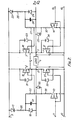
- switches 5', 6', 7' and 8' are field effect transistors, which, compared to bi-polar transistors, require minimal drive power and exhibit switching which for practical purpsoes, may be instantaneous.
- the d.c. voltage source corresponding to source 4 in Figure 1 is not shown, but the positive and negative terminals thereof are referenced 9 and 10 respectively.
- a control terminal 11, provided to receive a first control switching waveform, is connected directly to control FET transistor 6'.
- a control terminal 12 provided to receive a second control switching waveform is connected directly to control FET transistor 8'.
- transformers are not employed in order to drive transistors 5' and 7', which are connected to the positive side of the supply source. Instead the transistor switches 5' and 7 1 are controlled from control terminals 11 and 12 each via a further FET transistor, referenced 13 in the case of switch 5' and 14 in the case of switch 7'.
- transistor switch 5' consists of two diodes 17, 19 of which diode 19 is a zener diode, separated by a resistor 20 forming a series combination connected across the FET transistor 5' (i.e. between the drain and source electrodes). From a point between resistor 20 ardtdiode 19, bias is derived which is connected in combination with the drive signal from further FET transistor 13 to the gate electrode 15 of transistor 5'.
- Capacitor 21 and resistor 22 are provided for smoothing and attenuation.
- transistor switch 7' the series combination of two diodes 23, 24 of which diode 24 is a zener diode, separated by a resistor 25 is connected across the transistor 7' and bias is again derived from a point between resistor 25 and diode 24 and applied to the gate electrode 16 in similar manner. Again a capacitor 26 and a resistor 27 are provided for smoothing and attenuation.
- the bias voltage developed and applied to the gate 15 or 16 when the respective transistor 5' and 7' are conducting is the zener breakdown voltage of zener diodes 19 and 20. It is the provision of this bias which permits all of the devices to be controlled by two control switching waveforms (the relative phase of which may be adjustable in accordance with known practice) applied to the terminals 11 and 12, without requiring separate control, by way of transformers, of the transistors 5' and 7 1 which are connected to the positive terminal 10.
- the correct operation of the circuit relies upon the mean d.c. voltage level across the drain and source electrodes of the FET transistors 5' and 7' remaining at half of the supply level, but this is so for many inverter arrangements.
- field effect transistors 13 and 14 which may be low power transistors, also serve to ensure that transistors 5' and 7' are switched off coincidentally with the switching on of transistors 6' and 8' respectively.
- Diode 35 with resistor 28 and diode 29 with resistor 30 act as clamps to limit the value of the gate bias developed for transistors 5' and 7'.
- reversely polarised diodes 31, 32, 33 and 34 are connected across the transistors 5', 6', 7' and 8' as known per se.
Landscapes
- Engineering & Computer Science (AREA)
- Power Engineering (AREA)
- Inverter Devices (AREA)
Applications Claiming Priority (2)
| Application Number | Priority Date | Filing Date | Title |
|---|---|---|---|
| GB8013365 | 1980-04-23 | ||
| GB8013365A GB2074799A (en) | 1980-04-23 | 1980-04-23 | Transistor inverters |
Publications (1)
| Publication Number | Publication Date |
|---|---|
| EP0038624A1 true EP0038624A1 (de) | 1981-10-28 |
Family
ID=10512961
Family Applications (1)
| Application Number | Title | Priority Date | Filing Date |
|---|---|---|---|
| EP81301134A Withdrawn EP0038624A1 (de) | 1980-04-23 | 1981-03-18 | Massnahmen zur Verbesserung von Transistorumformerschaltungen |
Country Status (2)
| Country | Link |
|---|---|
| EP (1) | EP0038624A1 (de) |
| GB (1) | GB2074799A (de) |
Cited By (3)
| Publication number | Priority date | Publication date | Assignee | Title |
|---|---|---|---|---|
| DE3234602A1 (de) * | 1982-09-15 | 1984-03-22 | Licentia Gmbh | Wechselrichterschaltung |
| WO1988000770A1 (en) * | 1986-07-24 | 1988-01-28 | Robert Bosch Gmbh | Final stage of a bridge circuit |
| AT402868B (de) * | 1994-09-30 | 1997-09-25 | Fronius Schweissmasch | Stromquelle für die energieversorgung eines verbraucherkreises |
Families Citing this family (3)
| Publication number | Priority date | Publication date | Assignee | Title |
|---|---|---|---|---|
| EP0266394A4 (de) * | 1986-04-23 | 1988-09-07 | Mechanical Tech Inc | Leistungsverstärkermodul für einen rüttler. |
| JP2658427B2 (ja) * | 1989-01-17 | 1997-09-30 | 富士電機株式会社 | 電力変換用半導体素子のスナバ回路とそのモジュール装置 |
| US4965710A (en) * | 1989-11-16 | 1990-10-23 | International Rectifier Corporation | Insulated gate bipolar transistor power module |
-
1980
- 1980-04-23 GB GB8013365A patent/GB2074799A/en not_active Withdrawn
-
1981
- 1981-03-18 EP EP81301134A patent/EP0038624A1/de not_active Withdrawn
Non-Patent Citations (1)
| Title |
|---|
| Electronique et Applications Industrielles, No. 259, November 1978, Paris, FR FILLEAU, A.: "Applications des VMOS; la Puissance d'une Nouvelle Technologie", pages 19-24. * page 21, column 3, line 13 to page 22, column 3, line 27; figure 6 * * |
Cited By (3)
| Publication number | Priority date | Publication date | Assignee | Title |
|---|---|---|---|---|
| DE3234602A1 (de) * | 1982-09-15 | 1984-03-22 | Licentia Gmbh | Wechselrichterschaltung |
| WO1988000770A1 (en) * | 1986-07-24 | 1988-01-28 | Robert Bosch Gmbh | Final stage of a bridge circuit |
| AT402868B (de) * | 1994-09-30 | 1997-09-25 | Fronius Schweissmasch | Stromquelle für die energieversorgung eines verbraucherkreises |
Also Published As
| Publication number | Publication date |
|---|---|
| GB2074799A (en) | 1981-11-04 |
Similar Documents
| Publication | Publication Date | Title |
|---|---|---|
| DE69412414T2 (de) | Halbbrücken treiberschaltung | |
| US4068295A (en) | Voltage multiplier for an electronic time apparatus | |
| EP0048758B1 (de) | Feldeffekttransistor-schaltungsanordnung | |
| CA1121076A (en) | High voltage switch and capacitive drive | |
| GB2131635B (en) | Bridge rectifier circuit | |
| US3714470A (en) | Variable duty cycle signal generator | |
| US4970420A (en) | Power field effect transistor drive circuit | |
| KR940003156A (ko) | 전원 공급 회로와 그 회로를 갖춘 전기 장치 | |
| KR940011278B1 (ko) | 반도체 제어장치 | |
| EP0345679A3 (de) | Fehlerschutzschaltung für Stromversorgung | |
| EP0038624A1 (de) | Massnahmen zur Verbesserung von Transistorumformerschaltungen | |
| US4315307A (en) | Switching device and switched-type power supply using the same | |
| GB1570164A (en) | Current drive circuit | |
| US4908857A (en) | Isolated drive circuit | |
| US5508652A (en) | Transistor switching circuit | |
| US3938027A (en) | Electrical thyristor circuit | |
| KR900000644B1 (ko) | Fet게이트 구동회로 | |
| AU566128B2 (en) | Sample and hold circuit | |
| JPS6179321A (ja) | スイツチ装置 | |
| JPH051828Y2 (de) | ||
| GB1296230A (de) | ||
| JPH041582B2 (de) | ||
| US4099072A (en) | Variable pulse width circuit | |
| KR890003492Y1 (ko) | 뮤팅회로의 클램핑 보완회로 | |
| US4550365A (en) | Static semi-conductor electrical energy converter apparatus |
Legal Events
| Date | Code | Title | Description |
|---|---|---|---|
| PUAI | Public reference made under article 153(3) epc to a published international application that has entered the european phase |
Free format text: ORIGINAL CODE: 0009012 |
|
| AK | Designated contracting states |
Designated state(s): CH DE FR IT NL SE |
|
| STAA | Information on the status of an ep patent application or granted ep patent |
Free format text: STATUS: THE APPLICATION IS DEEMED TO BE WITHDRAWN |
|
| 18D | Application deemed to be withdrawn |
Effective date: 19821004 |
|
| RIN1 | Information on inventor provided before grant (corrected) |
Inventor name: BAINES, GEORGE WILLIAM |