EP0035926B1 - Système de commutation de signalisation dans un réseau de commutation temporelle, et réseau de commutation temporelle comportant un tel système - Google Patents
Système de commutation de signalisation dans un réseau de commutation temporelle, et réseau de commutation temporelle comportant un tel système Download PDFInfo
- Publication number
- EP0035926B1 EP0035926B1 EP81400289A EP81400289A EP0035926B1 EP 0035926 B1 EP0035926 B1 EP 0035926B1 EP 81400289 A EP81400289 A EP 81400289A EP 81400289 A EP81400289 A EP 81400289A EP 0035926 B1 EP0035926 B1 EP 0035926B1
- Authority
- EP
- European Patent Office
- Prior art keywords
- inputs
- outputs
- address
- signalisation
- register
- Prior art date
- Legal status (The legal status is an assumption and is not a legal conclusion. Google has not performed a legal analysis and makes no representation as to the accuracy of the status listed.)
- Expired
Links
- 230000011664 signaling Effects 0.000 title description 85
- 230000015654 memory Effects 0.000 claims description 68
- 230000002093 peripheral effect Effects 0.000 claims description 6
- 238000004891 communication Methods 0.000 claims description 4
- 238000000034 method Methods 0.000 claims description 4
- 238000011084 recovery Methods 0.000 claims 4
- 230000001360 synchronised effect Effects 0.000 description 14
- 230000004044 response Effects 0.000 description 6
- 230000000694 effects Effects 0.000 description 3
- 230000006870 function Effects 0.000 description 3
- 230000005540 biological transmission Effects 0.000 description 2
- 238000006243 chemical reaction Methods 0.000 description 2
- 230000033764 rhythmic process Effects 0.000 description 2
- 102000016252 Huntingtin Human genes 0.000 description 1
- 108050004784 Huntingtin Proteins 0.000 description 1
- 230000006978 adaptation Effects 0.000 description 1
- 230000000903 blocking effect Effects 0.000 description 1
- 125000004122 cyclic group Chemical group 0.000 description 1
- 238000013479 data entry Methods 0.000 description 1
- 238000001514 detection method Methods 0.000 description 1
- 238000010586 diagram Methods 0.000 description 1
- 235000021183 entrée Nutrition 0.000 description 1
- 238000012544 monitoring process Methods 0.000 description 1
- 230000002688 persistence Effects 0.000 description 1
- 230000003252 repetitive effect Effects 0.000 description 1
Images


Classifications
-
- H—ELECTRICITY
- H04—ELECTRIC COMMUNICATION TECHNIQUE
- H04Q—SELECTING
- H04Q11/00—Selecting arrangements for multiplex systems
- H04Q11/04—Selecting arrangements for multiplex systems for time-division multiplexing
Definitions
- the invention relates to a signaling switching system in a time switching network used in particular in telephone exchanges.
- a time switching network allows the exchange of communications between incoming trunks and outgoing trunks on which information is transmitted in pulse code modulation from the MIC.
- a MIC type junction comprises frames consisting of thirty-two time intervals, the first ITO and the seventeenth IT16 being assigned to signaling and are called signaling channels, and , whose time intervals IT1 to IT15 and IT17 to IT32 are allocated to thirty multiplexed simultaneous calls and are called speech channels; each of the time slots includes a sample of eight bits.
- the frames are grouped into multiframes which each include sixteen frames numbered from 0 to 15 and the ITO of each frame includes the frame alignment signaling (advice G 732 ⁇ 2.3 and 2.4).
- the IT16 time intervals are assigned to the channel-by-channel signaling relating to communications according to the following table in which the first four elements of the sample are designated by IT16A and the last four by IT16B.
- x being a reserve element fixed at 1 if it is not used, y indicating a loss of multiframe locking, a, b, c, d being binary signaling elements corresponding to each speech channel (advice G 732 ⁇ 4).
- the IT16 of the TRO frame contains the multiframe locking signaling (0000 xyxx).
- the switching of the speech channels is ensured by a connection network under the control of a central control unit comprising at least one computer and the signaling switching is ensured by a signaling unit or signalman which comprises a microprocessor working under the control of the central unit and which is connected to the connection network by at least one incoming signaling junction JSe and one outgoing signaling junction JSs which comprise all the signaling channels IT16 relating to the communication channels speech switched in the connection network.
- the content of the IT2 of the incoming junction Je4 is switched into the IT30 of the outgoing junction Js28 by the connection network, if we also want to switch signaling, the content of the associated signaling channel must be at IT2 and located in IT16A of frame 2 of the Je4 junction (see table above) is transferred in the signaling channel associated with IT30 and located in IT16 B of frame 14 of junction Js28.
- the signaling system comprises a central processor which processes the signaling information of channel 16 in a uniform manner, it also comprises a signaling controller which contributes to reducing the load of the central processor.
- the function of the signaling controller is to cyclically scan a random access memory comprising all the signaling data, to detect changes of state to carry out checks to validate the changes of state.
- This controller includes programmed logic that performs the most complex functions, namely assembling state change messages, analyzing orders from the central processor and generating pulsed signals.
- the controller also has wired logic that performs the most simple and highly repetitive tasks, namely cyclic reading of the memory which contains the signaling data, detection of changes. state, and monitoring the persistence of these state changes.
- the system according to the invention makes it possible to discharge the microprocessor of the signaling unit from switching the signaling channels by means of a wired logic, without blocking in the strict sense for usual capacities, with a very low and constant delay (without phase distortion) and, without path finding, according to claim 1.
- the time switching network shown diagrammatically in FIG. 1 essentially comprises a connection network 1 comprising at least one time switching stage and possibly one or more spatial switching stages, a network to which are connected N junctions JO to J (N.1) which each comprise an incoming junction I and a junction outgoing Js, a control unit 2 which comprises at least one computer which is connected to a bus 3 for access to the peripherals, a clock, and a programmed marking device 5 which is connected on the one hand to the bus 3 and secondly to the switching network 1 to which it provides the addresses of two channels in relationship, firstly that of an incoming channel ITxJe which means the xth path of eflower incoming trunk and secondly that an outgoing path ITyJs which designates the y iè path s me me iè outgoing trunk, x and y being between 0 and 31 and e and s is between 0 and N-1.
- a connection network 1 comprising at least one time switching stage and possibly one or more spatial switching stages, a network to which are
- this time switching network comprises a signaling unit 6 which is connected to the bus 3 via a programmed signaling device 7 and which is connected to the connection network via at least one signaling junction which includes an incoming JSe junction and an outgoing junction JSs, the connection network supplying it with a synchronization signal S1 relating to JSe and a synchronization signal S2 relating to JSs.
- This signaling unit is constituted by a microcomputer 8 which performs the functions of signaler, receiver and sender under the control of unit 2, and, according to the invention, by a signaling switching system 9 produced by means of wired logic which receives the signals JSe, S1 and S2 from the connection network 1, which supplies the signal JSs to it and which receives the addresses ITxJe and ITyJs of two related channels coming from the programmed marking device 5.
- the signaling switching system shown in fig. 2 corresponds to the case where the number N of junctions connected to the network is less than or equal to 32; in this case, a single signaling junction is sufficient to contain all the signaling information.
- the row of the frame of the JSe signaling junction (respectively JSs) is made to correspond to the rank of the incoming junction (respectively outgoing).
- the signaling junction JSe (respectively JSs) contains all the signaling information contained in the IT16 of the incoming junctions (respectively outgoing).
- the first ITO channel of the first TRO frame of JSe contains the sample of IT16 of the TRO frame of the incoming junction JeO
- the second or IT1 contains the IT16 of TRO de Jel
- IT31 contains Je16 TRO IT16.
- the second frame TR1 of JSe likewise contains the IT16 of the frames TR1 of the junctions Je0 to Je31 and so on, until the thirty-second frame TR31 of JSe which contains the IT16 of the frames TR31 of the junctions Je0 to Je31.
- JSs the first ITO channel of the first TRO frame of JSe contains the sample of IT16 of the TRO frame of the incoming junction JeO
- the second or IT1 contains the IT16 of TRO de Jel
- IT31 contains Je16 TRO IT16.
- the second frame TR1 of JSe likewise contains the IT16 of the frames TR1 of the junctions Je0 to Je31 and so on, until the thirty-second frame TR31 of JSe which contains the IT16 of the frames TR31 of
- the sixteen frames of a signaling junction which comprises 32 ⁇ 32 channels or 512 channels, can contain up to 1024 signaling information since each signaling information comprises four binary elements and each channel therefore comprises two signaling information .
- the system shown in fig. 2 includes a register 10 of eight binary elements with serial input and parallel outputs whose input receives the signal JSe from the incoming signaling junction and whose clock input receives the clock signal HO which corresponds to the transmission rate binary elements on the junctions and which is equal to 2 MHz in our example.
- It also includes a register 11 of four binary elements with parallel inputs and parallel outputs whose inputs are connected to the first four outputs of register 10 and whose clock input receives a clock signal H1 whose frequency is a quarter of that of the clock signal H0, that is to say 500 kHz in our example.
- This register 11 constitutes the data entry register of a signaling memory 12 which is a random access memory of 1024 words of four elements. binary elements, which corresponds to the maximum capacity of the signaling junction.
- the outputs of this memory 12 are connected to the inputs of a register 13 of four binary elements with parallel inputs and serial output whose clock input receives the signal HO and whose output provides the signal JSs of the outgoing signaling junction .
- the system includes an addressing multiplexer 14 of the signaling memory, the outputs of which are connected to the addressing inputs AD of the memory 12, these inputs AD being ten in number since the memory comprises 1024 words.
- the inputs of the multiplexer 14 which correspond to the writing of the signaling memory 12 are connected to the outputs of a writing address register 15 and those which correspond to the reading to the outputs of a reading address register 16.
- the registers 15 and 16 are registers of ten binary elements with parallel inputs and parallel outputs and the clock input of each of them receives the clock signal H1.
- the inputs of register 15 are connected to the outputs of a write addressing circuit 17 and those of register 16 to the outputs of a read addressing circuit 18.
- the write addressing circuit 17 firstly comprises a logic circuit 19 for detecting loss and resumption of multiframe locking, of which eight inputs are connected to the outputs of the register 10.
- a memory of rank of frame 20 which is a 32 word random access memory of eight binary elements, each word corresponding to one of the 32 incoming junctions and being subdivided into two parts, a first part comprising the first four binary elements which corresponds to the rank of frame among the sixteen frames of the multiframe of each of these junctions, and a second part comprising the last four binary elements which corresponds to indications concerning the locking of multiframe, that is to say the synchronization of multiframe.
- the first four inputs of the frame rank memory 20 are connected to the outputs of a multiplexer 21, four of the eight inputs of which are connected to four outputs of the logic circuit 19 and the control input of which is connected to another output of the logic circuit 19.
- the first four outputs of memory 20 are connected on the one hand to the four most significant inputs of the write address register 15 and on the other hand to the inputs of an incrementation circuit 22 which increments the frame rank coded on four bits it receives by one, and whose outputs are connected to the other four inputs of the multiplexer 21.
- the last four inputs of the frame rank memory 20 are connected to four outputs of the logic circuit 19 and the last four outputs are connected to four inputs of this logic circuit 19.
- the write addressing circuit 17 includes a counter 23 with six binary elements numbered from 0 to 5; on the one hand, the six outputs of the counter 23 are connected to the first six inputs of the write address register, on the other hand the outputs n ° 1 to 5 are connected to the addressing inputs AD of the memory 20. Finally, the clock input of counter 23 receives the signal H1 and the reset input the signal S1 of synchronism with the incoming junction.
- the read addressing circuit 18 comprises, first of all, an address memory 24 which is a random access memory of 1024 words of ten binary elements and the outputs of which are connected to the inputs of the read address register 16.
- a storage register 25 of ten binary elements numbered 0 to 9 receives from the programmed marking device the address ITxJe of an incoming channel, the five least significant binary elements n ° 0 to 4 giving the address d 'an incoming junction Je among thirty-two and the five most significant binary elements n ° 5 to 9 giving the address of an ITx channel among thirty-two on this junction Je.
- the i th output of this register 25 (with 0 ⁇ i ⁇ 9) is connected to the [(i + 1) modulo 1O] th input of the address memory 24.
- a storage register 26 of ten binary elements numbered from 0 to 9 receives from the programmed marking device the address of an outgoing channel ITyJs in relation to the incoming channel whose address is contained in register 25, binary elements n ° 0 to 4 giving the address of an outgoing Js junction among thirty-two and binary elements n ° 5 to 9 giving the address of an ITy channel among thirty-two on this Js junction.
- the ten addressing inputs AD of the memory 24 are connected to the outputs of an addressing multiplexer 27.
- the inputs of the multiplexer 27 which correspond to the addressing in writing of the memory 24 are connected to the outputs of the register 26 of such so that the i th output of this register is connected to the [(i + 1) modulo 10] th addressing input.
- the inputs of the multiplexer 27 which correspond to the addressing in reading of the memory 24 are connected to the outputs of a computer 28 of ten binary elements whose clock input receives the signal H1, including the reset input receives the signal S2 of synchronism with the outgoing junction, this signal S2 coming from the connection network, and the outputs of which are connected to the inputs of the multiplexer 27 which correspond to the addressing in reading of the memory 24 so that the i th the counter output (0 ⁇ i ⁇ 9) is connected to the i th addressing input.
- the memories 12 and 24 as well as the associated addressing multiplexers 14 and 27 each receive at their write / read command input E / L the clock signal H1 which makes it possible to share each period of 2 they in a half period of 1 they for writing and a half period of 1 ⁇ s for reading.
- the frame rank memory 20 receives at its write / read command input E / L a signal H2 the frequency of which is half that of the signal H1 that the address counter 23 receives, this is -to say that the frequency of H2 is 250 kHz in our example, so that for each addressing of the memory 20, there is a half-period of 2 ⁇ s for writing and a half-period of 2 ⁇ s for reading.
- the signaling switching system consists, first of all, in writing each signaling information in a signaling memory at an address which consists firstly of four binary elements, which give the rank of the frame at which belongs the signaling information on JSe, secondly by five binary elements which give the number of the time interval (or channel) to which the signaling information belongs to JSe, and, thirdly by a binary element which indicates whether the information belongs to part A or part B of the time interval.
- the signaling information contained in the signaling memory is read so as to reconstruct an outgoing signaling junction JSs in accordance with the indications in the table on page 2 and the correspondence information provided by the programmed marking device.
- the speech channel number in binary code alone gives the half-part and frame number of IT16 associated.
- the first binary element of the number of the speech channel in binary code is equal to 0 or 1 according to whether one associates part A or part B of IT16 and the last four binary elements give in binary code the number of the frame to which the associated IT16 belongs; moreover, given the structure of a signaling junction (see page 5, lines 16 to 34), the signaling information which relates to the i th incoming junction (respectively outgoing) is located in the i th intervals of the incoming signaling junction (respectively outgoing).
- the register 10 On the incoming signaling junction JSe the binary elements are transmitted at the rate of 2 MHz, the register 10 performs a series-parallel conversion and it supplies at the frequency H1 of 500 kHz (500 kHz is equal to 2 MHz divided by four), that is to say every two microseconds, signaling information comprising four binary elements at the input of the signaling memory 12 via the register 11.
- This information is written into the signaling memory 12 under the control of the write-read signal which is the signal H1, thus during each period of two microseconds, one microsecond is devoted to writing and the other to the reading.
- This information is entered at the write address defined in the description of the principle above, this address being produced by the write circuit 17 and arriving at the addressing inputs AD of 12 via the multiplexer 14 and register 15 every two microseconds, since 14 and 15 receive the clock signal H1 at 500 kHz.
- the write circuit must first establish the rank of the frame concerned for each incoming junction, this is why it includes a circuit 19 for detecting loss and resumption of multi locking.
- - frame which makes it possible to detect the start of multiframe thanks to the IT16 of the TRO frame, which contains the multiframe locking code, and to note the passages from the desynchronized state to the synchronized state.
- This algorithm is performed by the circuit 19 associated with the second part of the memory 20, each word of which corresponds to an incoming junction.
- the last four bits of words in memory 20 have the following meanings: the fifth means “junction synchronized or not ", the sixth means” the ltl6 of a TRO frame is different from zero or not ", the seventh means ccl'IT16 of a frame is different from zero or not”, and the eighth gives the logical sum partial IT16 of the current multiframe.
- the frame rank memory 20 is read every four microseconds, since the write-read command input receives the signal H2 of frequency 250 kHz; on the other hand, given the addressing of this memory 20, the same address is present at the inputs AD of 20 during each period of four microseconds which is broken down into two microseconds dedicated to reading and two microseconds to writing.
- the logic 19 proceeds, via the multiplexer 21, to register the frame rank in the first part of the memory 20 at the address corresponding to this incoming junction.
- the multiplexer 21 In the synchronized state of a junction, after each reading of the corresponding frame rank, the frame rank which has just been read, increased by one unit by the circuit 22, is written at the same address, the multiplexer 21 being positioned by the logic 19 so as to present at the input of the first part of the memory 20 the signals coming from the circuit 22.
- the first part of the write address is thus established, which indicates the frame rank using four binary elements.
- the other six bits of the write address are provided by the outputs of counter 23; on the one hand, outputs n ° 1 to 5 give the rank of the time interval present in input on JSe (synchronism being ensured by signal S1), that is to say given the constitution of the signaling channel the rank of the incoming junction, on the other hand the output n ° 0 indicates whether it is the first part A or the second part B of the time interval.
- the signaling information is read from the signaling memory 12 during each half-period of a microsecond dedicated to reading. This information is read at the read address defined in the description of the principle above, this address being produced by the read circuit 18 and arriving at the addressing inputs AD of 12 via the multiplexer 14 and the register 16, every two microseconds, since 14 and 16 receive the clock signal H1 at 500 kHz.
- the means for developing the reading address in accordance with the principle set out above consist in writing, in the address memory 24, the word abcdefghij corresponding to the incoming channel ITxJe of address jabcdefghi and obtained by means of the particular wiring. described above between the outputs of register 25 containing the address of ITxJe and the inputs of memory 24, at the address pqrstuvwxy corresponding to the outgoing junction channel ITyJs of address ypqrstuvwx and obtained by means of the specific wiring described above above between the outputs of register 26 containing the address of ITyJs and the inputs of the addressing multiplexer which correspond to the writing.
- the outgoing signaling channel is constituted by addressing the memory 24 in read mode by the output signals from the counter 28, in synchronism with the network. connection thanks to signal S2.
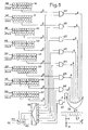
- Fig. 4 represents an exemplary embodiment having the same principle as the preceding exemplary embodiment, but which is adapted to a number N of incoming junctions and outgoing junctions greater than 32 and at most equal to 256.
- Fig. 4 shows the adaptations which make it possible to go from 32 junctions to 256 junctions.
- the system comprises an input circuit which is a serial-parallel converter 30 whose inputs are connected to the incoming signaling junctions JSeO to JSe7 and which receives the clock signal H0, a register 31 identical to the register 11 in FIG. 2, the four inputs of which are connected to four outputs of the converter 30 and which receives as clock inputs a clock signal H3 of frequency 4 MHz eight times greater than that received by the register 21 since there are eight times more information for a given time.
- a serial-parallel converter 30 whose inputs are connected to the incoming signaling junctions JSeO to JSe7 and which receives the clock signal H0
- a register 31 identical to the register 11 in FIG. 2, the four inputs of which are connected to four outputs of the converter 30 and which receives as clock inputs a clock signal H3 of frequency 4 MHz eight times greater than that received by the register 21 since there are eight times more information for a given time.
- the system includes a signaling memory of 8192 (8x1024) words of four binary elements, the inputs of which are connected to the outputs of register 31, of which the input of write / read command E / L receives the signal. H3, and, the outputs of which are connected to the inputs of a serial-parallel converter 33, the outputs of which provide the outgoing signaling junctions JSsO to JSs7 and which receives the clock signal HO.
- the thirteen addressing inputs AD of the signaling memory 32 are connected to the outputs of a multiplexer 34 whose control input receives the signal H3, whose inputs which correspond to the writing are connected to the outputs of a register write address 35 of thirteen binary elements and whose inputs which correspond to the reading are connected to the outputs of a read address register 36 of thirteen binary elements.
- register 35 The inputs of register 35 are connected to the outputs of a write addressing circuit 37, those of register 36 are connected to the outputs of a read addressing circuit 38 and the clock input of each of these registers receives the clock signal H3.
- the write addressing circuit 37 comprises a logic circuit 39 for detecting loss and resumption of multiframe locking, identical to logic circuit 19, eight inputs of which are connected to the outputs of register 30.
- a memory of frame rank 40 which is a random access memory of 256 (8x32) words of eight binary elements each word of which corresponds to one of the 256 incoming junctions whose write / read command input E / L receives the signal d clock H0, a multiplexer 41, identical to the multiplexer 21, and an incrementation circuit 42, identical to the circuit 22, the connections between the elements 39, 40, 41 and 42 being identical to those between the elements 19,20,21 and 22.
- Circuit 37 finally comprises a counter 43 with nine binary elements numbered from 0 to 8; on the one hand, the nine outputs of the counter 43 are connected to the nine least significant inputs of the write address register, on the other hand, the outputs n ° 1 to 8 are connected to the addressing inputs AD of memory 40.
- the clock input of counter 43 receives the signal H3 and the reset input the signal S1 of synchronism with the incoming junctions.
- the read addressing circuit 38 comprises, first of all, an address memory 44 which is a random access memory of 8192 (8x1024) words of thirteen binary elements and the outputs of which are connected to the inputs of the address register of reading 36.
- a storage register 45 of thirteen binary elements numbered 0 to 12 receives from the programmed marking device the address of an incoming channel lTxJe the eight least significant binary elements n ° 0 to 7 giving the address of an incoming junction Je among two hundred and fifty-six and the five most significant binary elements give the address of a channel ITx among thirty-two on this junction Je.
- the i th output of this register 45 (with 0 i i 12 12) is connected to the [(i + 1) modulo 13] th input of the address memory 44.
- a storage register 46 of thirteen binary elements numbered from 0 to 12 receives from the programmed marking device the address of an outgoing channel ITyJs in relation to the incoming channel whose address is contained in register 45, the eight least significant bits n ° 0 to 7 giving the address of an outgoing junction Js among two hundred fifty-six and the five most significant bits n ° 8 to 12 giving the address of a ITy route among thirty-two on this Js junction.
- the thirteen addressing inputs AD of memory 44 are connected to the outputs of an addressing multiplexer 47.
- the inputs of the addressing multiplexer 47 which correspond to write addressing are connected to the outputs of register 26 so that the ith output of this register 46 (with 0 ⁇ i ⁇ 12) is connected to the [(i + l) mod 13] I meentrée addressing.
- the inputs of the multiplexer 47 which correspond to the read addressing of the memory 44 are connected to the outputs of a counter 48 of thirteen binary elements whose clock input receives the signal H3, including the reset input. zero receives the signal 52 synchronous with the outgoing junctions and whose outputs are connected to the inputs of the multiplexer 47 corresponding to the read addressing so that the ith output of the counter is connected to the input I ie me to addressing (with 0 ⁇ 1 ⁇ 13).
- the write / read control input E / L of the memory 44 and the control input of the multiplexer 47 receive the clock signal H3.
- Fig. 5 represents a serial-parallel converter 30 which comprises a set of eight shift registers 50 to 57 with serial input and eight parallel outputs, the inputs of which are connected respectively to the junctions JSeO to JSe7 and the clock inputs of which receive the signal H0 .
- the registers 50 and 51 comprise eight binary elements, the registers 52 and 53 nine, the registers 54 and 55 ten and the registers 56 and 57 eleven, the eight most significant binary elements of each register being those available on the eight outputs.
- each register is respectively connected to the “AND” logic gates 60 to 67 which are each the symbolic representation of a set of eight “AND” logic gates and the other inputs of which are connected to the outputs of a decoder 58.
- This decoder 58 has three inputs connected respectively to outputs n ° 0, 1 and 2 of the counter 43 of the writing circuit, and, eight outputs n ° 0 to 7 connected respectively to the logic gates "AND” 60 to 67, which it " cyclically opens every 250 ns since counter 43 receives the H3 clock signal (4 MHz).
- a logic “OR” gate 59 symbolically represented, has eight times eight inputs connected to the eight outputs of each of the eight “AND” gates 60 to 67 and has eight outputs which are connected to logic 39 and the first four of which are also connected to register entries 31.
- the information is shifted in registers 50 to 57 at the HO (2 MHz) rhythm when it arrives at the junctions. Every four elementary times, ie 4 ⁇ 500 ns, a half time interval, that is to say signaling information is available at the output of each register.
- the decoder 58 successively "opens" the doors 60 and 61. At the end of this first period a new offset occurs and the half-intervals of time progress by one binary element in each register, half time intervals are then available on the outputs of registers 52 and 53.
- the decoder 58 successively "opens" the doors 62 and 63. At the end of this second period a new offset occurs and the half time intervals progress again by one binary element in each register, half time intervals are then available on the outputs of registers 54 and 55.
- the decoder 58 successively "opens" gates 64 and 65. At the end of this third period a new offset occurs and the half time intervals again progress by one binary element in each register, half time intervals are available on the outputs of registers 56 and 57.
- the decoder 58 successively "opens" gates 66 and 67. At the end of this fourth period a new offset occurs and the half time intervals progress again by one binary element in each register.
- Fig. 6 shows a parallel-to-serial converter 33 which comprises a set of eight shift registers 70 to 77 with four parallel inputs and serial output, the outputs of which are connected respectively to the junctions JSsO to JSs7 and the clock inputs of which receive the signal H0 .
- the registers 70 and 71 have seven binary elements, the registers 72 and 73 six, the registers 74 and 75 five and the registers 76 and 77 four, the four least significant elements n ° 0 to 3 of each register being those which receive the input signals.
- each register is respectively connected to the outputs of logic gates "AND” 80 to 87, which are each the symbolic representation of four logic gates “AND” and whose inputs are connected on the one hand to the outputs of the signaling memory 32 which provides a half-interval every 250 nanoseconds (ns) and on the other hand to the outputs of a decoder 78.
- This decoder 78 has three inputs connected to outputs n ° 0 to 2 of the counter 48 of the read circuit 38, and, has eight outputs n ° 0 to 7 connected respectively to the logic gates "AND” 80 to 87, which it "opens” in turn cyclically every 250 ns since the counter 48 receives for clock signal the signal H3 of frequency 4 MHz.
- the decoder 78 successively "opens" the gate 80 and the gate 81 which has the effect of storing two half time intervals from the memory 32 respectively in the four least significant binary elements n ° 0 to 4 of registers 70 and 71. At the end of this first period an offset occurs and the half time intervals progress by one binary element in each register.
- the decoder 78 successively "opens" the gate 82 and the gate 83, which has the effect of storing two half time intervals from the memory 32 respectively in the four least significant binary elements Nos. 0 to 4 of registers 72 and 73. At the end of this second period, an offset occurs and the half time intervals progress again by one binary element in each register.
- the decoder 78 successively "opens" the door 84 and the door 85 which has the consequence of storing two half time intervals from the memory 32 respectively in the four least significant binary elements n ° 0 to 4 of registers 74 and 75. At the end of this third period, an offset occurs and the half time intervals progress again by one binary element in each register.
- the decoder 78 successively "opens" the door 86 and the door 87, which has the effect of storing two half time intervals respectively in the registers 76 and 77.
Landscapes
- Engineering & Computer Science (AREA)
- Computer Networks & Wireless Communication (AREA)
- Use Of Switch Circuits For Exchanges And Methods Of Control Of Multiplex Exchanges (AREA)
Applications Claiming Priority (2)
| Application Number | Priority Date | Filing Date | Title |
|---|---|---|---|
| FR8005417 | 1980-03-11 | ||
| FR8005417A FR2478415B1 (fr) | 1980-03-11 | 1980-03-11 | Systeme de commutation de signalisation dans un reseau de commutation temporelle, et reseau de commutation temporelle comportant un tel systeme |
Publications (2)
| Publication Number | Publication Date |
|---|---|
| EP0035926A1 EP0035926A1 (fr) | 1981-09-16 |
| EP0035926B1 true EP0035926B1 (fr) | 1983-08-10 |
Family
ID=9239538
Family Applications (1)
| Application Number | Title | Priority Date | Filing Date |
|---|---|---|---|
| EP81400289A Expired EP0035926B1 (fr) | 1980-03-11 | 1981-02-24 | Système de commutation de signalisation dans un réseau de commutation temporelle, et réseau de commutation temporelle comportant un tel système |
Country Status (6)
| Country | Link |
|---|---|
| US (1) | US4402078A (Sortimente) |
| EP (1) | EP0035926B1 (Sortimente) |
| BR (1) | BR8101429A (Sortimente) |
| DE (1) | DE3160737D1 (Sortimente) |
| FR (1) | FR2478415B1 (Sortimente) |
| GR (1) | GR74146B (Sortimente) |
Families Citing this family (8)
| Publication number | Priority date | Publication date | Assignee | Title |
|---|---|---|---|---|
| IT1155660B (it) * | 1982-03-24 | 1987-01-28 | Cselt Centro Studi Lab Telecom | Perfezionamenti alle matrici elementari di commutazione pcm |
| FR2551939B1 (fr) * | 1983-09-14 | 1985-10-11 | Cit Alcatel | Dispositif de transfert et de traitement de voies de donnees ou de signalisation d'un ensemble de lignes multiplex |
| EP0164105A3 (de) * | 1984-06-04 | 1988-01-27 | Siemens Aktiengesellschaft | Schaltungsanordnung zur Aufnahme und/oder zur Abgabe von seriell auftretenden Binärsignalen in bzw. von einer einen Mikrocomputer bzw. Mikroprozessor enthaltenden Verarbeitungseinrichtung |
| US4695974A (en) * | 1984-06-04 | 1987-09-22 | Siemens Aktiengesellschaft | Circuit arrangement for receiving and/or transmitting binary signals serially appearing on the plurality of lines to and from a processing device containing a micro-computer or microprocessor |
| FR2589656B1 (fr) * | 1985-07-03 | 1987-12-11 | Servel Michel | Procede et dispositif de conversion de multitrame de canaux numeriques en multitrame de paquets |
| JPH0779514B2 (ja) * | 1986-01-24 | 1995-08-23 | 日本電気株式会社 | 時分割時間スイツチ制御方式 |
| DE68916413T2 (de) * | 1989-03-14 | 1995-01-26 | Ibm | Vermittlungssystem für den gleichzeitigen Datentransfer zwischen Datenprozessoren. |
| US5058109A (en) * | 1989-06-28 | 1991-10-15 | Digital Equipment Corporation | Exclusionary network adapter apparatus and related method |
Citations (6)
| Publication number | Priority date | Publication date | Assignee | Title |
|---|---|---|---|---|
| FR2283605A1 (fr) * | 1974-08-30 | 1976-03-26 | Duquesne Jean | Unite de brassage pour voies numeriques |
| FR2295664A1 (fr) * | 1974-12-19 | 1976-07-16 | Sits Soc It Telecom Siemens | Unite de controle de signalisation, notamment pour central telephonique de transit |
| FR2347841A1 (fr) * | 1976-04-07 | 1977-11-04 | Labo Cent Telecommunicat | Transfert de la signalisation de ligne dans un central mic |
| FR2365922A1 (fr) * | 1976-09-24 | 1978-04-21 | Materiel Telephonique | Unite de signalisation pour central telephonique |
| FR2376572A1 (fr) * | 1976-12-30 | 1978-07-28 | Roche Alain | Circuits de conversion serie-parallele et de multiplexage ou de conversion parallele-serie et de demultiplexage pour des multiplex numeriques |
| GB2007942A (en) * | 1977-11-07 | 1979-05-23 | Post Office | Improvements in or relating to the switching of digital signals |
Family Cites Families (4)
| Publication number | Priority date | Publication date | Assignee | Title |
|---|---|---|---|---|
| SE383674B (sv) * | 1975-04-28 | 1976-03-22 | Ellemtel Utvecklings Ab | Sett och anordning for adressering av ett buffertminne i en formedlingsstation for synkrona datasignaler |
| US4156796A (en) * | 1977-11-29 | 1979-05-29 | International Business Machines Corporation | Programmable data processing communications multiplexer |
| FR2413008B1 (fr) * | 1977-12-22 | 1985-07-05 | Constr Telephoniques | Systeme de transfert de signaux pour centre de commutation temporelle |
| US4228536A (en) * | 1979-05-29 | 1980-10-14 | Redcom Laboratories, Inc. | Time division digital communication system |
-
1980
- 1980-03-11 FR FR8005417A patent/FR2478415B1/fr not_active Expired
-
1981
- 1981-02-24 EP EP81400289A patent/EP0035926B1/fr not_active Expired
- 1981-02-24 DE DE8181400289T patent/DE3160737D1/de not_active Expired
- 1981-03-10 US US06/242,304 patent/US4402078A/en not_active Expired - Fee Related
- 1981-03-11 BR BR8101429A patent/BR8101429A/pt unknown
- 1981-03-11 GR GR64372A patent/GR74146B/el unknown
Patent Citations (6)
| Publication number | Priority date | Publication date | Assignee | Title |
|---|---|---|---|---|
| FR2283605A1 (fr) * | 1974-08-30 | 1976-03-26 | Duquesne Jean | Unite de brassage pour voies numeriques |
| FR2295664A1 (fr) * | 1974-12-19 | 1976-07-16 | Sits Soc It Telecom Siemens | Unite de controle de signalisation, notamment pour central telephonique de transit |
| FR2347841A1 (fr) * | 1976-04-07 | 1977-11-04 | Labo Cent Telecommunicat | Transfert de la signalisation de ligne dans un central mic |
| FR2365922A1 (fr) * | 1976-09-24 | 1978-04-21 | Materiel Telephonique | Unite de signalisation pour central telephonique |
| FR2376572A1 (fr) * | 1976-12-30 | 1978-07-28 | Roche Alain | Circuits de conversion serie-parallele et de multiplexage ou de conversion parallele-serie et de demultiplexage pour des multiplex numeriques |
| GB2007942A (en) * | 1977-11-07 | 1979-05-23 | Post Office | Improvements in or relating to the switching of digital signals |
Non-Patent Citations (1)
| Title |
|---|
| COLLOQUE INTERNATIONAL DE COMMUTATION, mai 1979 Paris, FR LE PABIC et al.: "Utilisation des microprocesseurs dans les centraux de la gamme temporelle MT", pages 745-750 * |
Also Published As
| Publication number | Publication date |
|---|---|
| FR2478415A1 (fr) | 1981-09-18 |
| FR2478415B1 (fr) | 1986-12-05 |
| GR74146B (Sortimente) | 1984-06-06 |
| BR8101429A (pt) | 1981-09-15 |
| EP0035926A1 (fr) | 1981-09-16 |
| DE3160737D1 (en) | 1983-09-15 |
| US4402078A (en) | 1983-08-30 |
Similar Documents
| Publication | Publication Date | Title |
|---|---|---|
| JPH0439820B2 (Sortimente) | ||
| EP0057628B1 (fr) | Système de commutation numérique à division du temps de canaux en mode-circuit et en mode-paquet | |
| US4450557A (en) | Switching network for use in a time division multiplex system | |
| EP0041001B1 (fr) | Perfectionnements aux réseaux de commutation numérique à division du temps bit à bit | |
| EP0036808A1 (fr) | Concentrateur de système de communication pour relier plusieurs terminaux asynchrones de téléinformatique | |
| EP0035926B1 (fr) | Système de commutation de signalisation dans un réseau de commutation temporelle, et réseau de commutation temporelle comportant un tel système | |
| US3971891A (en) | Adaptable time division switch | |
| US3967070A (en) | Memory operation for 3-way communications | |
| EP0208604B1 (fr) | Procédé et dispositif de conversion de multitrame de canaux numériques en multitrame de paquets | |
| EP0112425B1 (fr) | Réseau de connexion temps-espace-temps utilisant une liaison en boucle fermée | |
| US3978290A (en) | Digital private automatic branch exchange | |
| EP0020255A1 (fr) | Niveau de commutation d'un opérateur pour réseau de commutation de données numériques par paquets | |
| EP0111792B1 (fr) | Dispositif de traitement de signalisation voie par voie pour autocommutateur temporel | |
| ATE311079T1 (de) | Unterraten-fernmeldevermittlungsanlage | |
| EP0141956B1 (fr) | Dispositif de transfert et de traitement de voies de données ou de signalisation d'un ensemble de lignes multiplex | |
| EP0018615B1 (fr) | Dispositif de raccordement de multiplex dans un central de commutation temporelle | |
| EP0301934B1 (fr) | Système de commutation temporel de paquets de différentes longueurs | |
| EP0091338B1 (fr) | Central téléphonique numérique modulaire étendu | |
| FR2715261A1 (fr) | Procédé et appareil de réduction de la puissance consommée dans des commutateurs de type temporel-spatial. | |
| EP0078634B1 (en) | Switching network for use in a time division multiplex system | |
| EP0230847B1 (fr) | Système de commutation de multiplex de paquets | |
| EP0042329A1 (fr) | Interface de passage d'une liaison de transmission numérique en mode MIC à une liaison de transmission numérique en mode Paquets et opérateur de commutation comportant une telle interface | |
| EP0025753A1 (fr) | Interface de passage à une liaison de transmission en mode "paquets" à partir d'une liaison de transmission numérique d'un autre mode | |
| SU1177936A1 (ru) | Устройство дл коммутации телеграфных каналов | |
| EP0091362B1 (fr) | Central téléphonique numérique modulaire généralisé |
Legal Events
| Date | Code | Title | Description |
|---|---|---|---|
| PUAI | Public reference made under article 153(3) epc to a published international application that has entered the european phase |
Free format text: ORIGINAL CODE: 0009012 |
|
| AK | Designated contracting states |
Designated state(s): BE DE LU |
|
| 17P | Request for examination filed |
Effective date: 19811012 |
|
| RBV | Designated contracting states (corrected) |
Designated state(s): BE DE LU |
|
| GRAA | (expected) grant |
Free format text: ORIGINAL CODE: 0009210 |
|
| AK | Designated contracting states |
Designated state(s): BE DE LU |
|
| REF | Corresponds to: |
Ref document number: 3160737 Country of ref document: DE Date of ref document: 19830915 |
|
| PLBE | No opposition filed within time limit |
Free format text: ORIGINAL CODE: 0009261 |
|
| STAA | Information on the status of an ep patent application or granted ep patent |
Free format text: STATUS: NO OPPOSITION FILED WITHIN TIME LIMIT |
|
| 26N | No opposition filed | ||
| PGFP | Annual fee paid to national office [announced via postgrant information from national office to epo] |
Ref country code: LU Payment date: 19910208 Year of fee payment: 11 |
|
| EPTA | Lu: last paid annual fee | ||
| PGFP | Annual fee paid to national office [announced via postgrant information from national office to epo] |
Ref country code: BE Payment date: 19920129 Year of fee payment: 12 |
|
| PGFP | Annual fee paid to national office [announced via postgrant information from national office to epo] |
Ref country code: DE Payment date: 19920218 Year of fee payment: 12 |
|
| PG25 | Lapsed in a contracting state [announced via postgrant information from national office to epo] |
Ref country code: LU Free format text: LAPSE BECAUSE OF NON-PAYMENT OF DUE FEES Effective date: 19920224 |
|
| PG25 | Lapsed in a contracting state [announced via postgrant information from national office to epo] |
Ref country code: BE Effective date: 19930228 |
|
| BERE | Be: lapsed |
Owner name: THOMSON-CSF TELEPHONE Effective date: 19930228 |
|
| PG25 | Lapsed in a contracting state [announced via postgrant information from national office to epo] |
Ref country code: DE Effective date: 19931103 |