EP0035767A1 - Semiconductor device - Google Patents
Semiconductor device Download PDFInfo
- Publication number
- EP0035767A1 EP0035767A1 EP81101619A EP81101619A EP0035767A1 EP 0035767 A1 EP0035767 A1 EP 0035767A1 EP 81101619 A EP81101619 A EP 81101619A EP 81101619 A EP81101619 A EP 81101619A EP 0035767 A1 EP0035767 A1 EP 0035767A1
- Authority
- EP
- European Patent Office
- Prior art keywords
- semiconductor
- control element
- component
- current
- monitoring
- Prior art date
- Legal status (The legal status is an assumption and is not a legal conclusion. Google has not performed a legal analysis and makes no representation as to the accuracy of the status listed.)
- Granted
Links
- 239000004065 semiconductor Substances 0.000 title claims abstract description 69
- 230000005855 radiation Effects 0.000 claims abstract description 18
- 230000006798 recombination Effects 0.000 claims abstract description 10
- 238000005215 recombination Methods 0.000 claims abstract description 10
- 239000000463 material Substances 0.000 claims abstract description 6
- 230000000694 effects Effects 0.000 claims abstract description 4
- 238000012544 monitoring process Methods 0.000 claims description 20
- 230000000903 blocking effect Effects 0.000 claims description 4
- 230000008859 change Effects 0.000 claims description 3
- 230000005540 biological transmission Effects 0.000 claims description 2
- 239000004020 conductor Substances 0.000 description 4
- 230000008878 coupling Effects 0.000 description 3
- 238000010168 coupling process Methods 0.000 description 3
- 238000005859 coupling reaction Methods 0.000 description 3
- 238000001816 cooling Methods 0.000 description 2
- 239000011810 insulating material Substances 0.000 description 2
- 239000002184 metal Substances 0.000 description 2
- 229910052751 metal Inorganic materials 0.000 description 2
- 239000010453 quartz Substances 0.000 description 2
- VYPSYNLAJGMNEJ-UHFFFAOYSA-N silicon dioxide Inorganic materials O=[Si]=O VYPSYNLAJGMNEJ-UHFFFAOYSA-N 0.000 description 2
- 238000005476 soldering Methods 0.000 description 2
- 230000007704 transition Effects 0.000 description 2
- RYGMFSIKBFXOCR-UHFFFAOYSA-N Copper Chemical compound [Cu] RYGMFSIKBFXOCR-UHFFFAOYSA-N 0.000 description 1
- 238000002679 ablation Methods 0.000 description 1
- 239000000853 adhesive Substances 0.000 description 1
- 238000004026 adhesive bonding Methods 0.000 description 1
- 230000001070 adhesive effect Effects 0.000 description 1
- 230000008901 benefit Effects 0.000 description 1
- 239000000919 ceramic Substances 0.000 description 1
- 229910052802 copper Inorganic materials 0.000 description 1
- 239000010949 copper Substances 0.000 description 1
- 230000006866 deterioration Effects 0.000 description 1
- 238000005530 etching Methods 0.000 description 1
- 238000004519 manufacturing process Methods 0.000 description 1
- 238000005259 measurement Methods 0.000 description 1
- 238000000034 method Methods 0.000 description 1
- 238000012806 monitoring device Methods 0.000 description 1
- 239000011224 oxide ceramic Substances 0.000 description 1
- 229910052574 oxide ceramic Inorganic materials 0.000 description 1
- 230000008569 process Effects 0.000 description 1
- 239000011253 protective coating Substances 0.000 description 1
- 230000004044 response Effects 0.000 description 1
- 238000003466 welding Methods 0.000 description 1
Images

Classifications
-
- H—ELECTRICITY
- H01—ELECTRIC ELEMENTS
- H01L—SEMICONDUCTOR DEVICES NOT COVERED BY CLASS H10
- H01L23/00—Details of semiconductor or other solid state devices
- H01L23/58—Structural electrical arrangements for semiconductor devices not otherwise provided for, e.g. in combination with batteries
-
- H—ELECTRICITY
- H02—GENERATION; CONVERSION OR DISTRIBUTION OF ELECTRIC POWER
- H02H—EMERGENCY PROTECTIVE CIRCUIT ARRANGEMENTS
- H02H7/00—Emergency protective circuit arrangements specially adapted for specific types of electric machines or apparatus or for sectionalised protection of cable or line systems, and effecting automatic switching in the event of an undesired change from normal working conditions
- H02H7/20—Emergency protective circuit arrangements specially adapted for specific types of electric machines or apparatus or for sectionalised protection of cable or line systems, and effecting automatic switching in the event of an undesired change from normal working conditions for electronic equipment
- H02H7/205—Emergency protective circuit arrangements specially adapted for specific types of electric machines or apparatus or for sectionalised protection of cable or line systems, and effecting automatic switching in the event of an undesired change from normal working conditions for electronic equipment for controlled semi-conductors which are not included in a specific circuit arrangement
-
- H—ELECTRICITY
- H03—ELECTRONIC CIRCUITRY
- H03K—PULSE TECHNIQUE
- H03K17/00—Electronic switching or gating, i.e. not by contact-making and –breaking
- H03K17/08—Modifications for protecting switching circuit against overcurrent or overvoltage
- H03K17/082—Modifications for protecting switching circuit against overcurrent or overvoltage by feedback from the output to the control circuit
- H03K17/0826—Modifications for protecting switching circuit against overcurrent or overvoltage by feedback from the output to the control circuit in bipolar transistor switches
-
- H—ELECTRICITY
- H01—ELECTRIC ELEMENTS
- H01L—SEMICONDUCTOR DEVICES NOT COVERED BY CLASS H10
- H01L2924/00—Indexing scheme for arrangements or methods for connecting or disconnecting semiconductor or solid-state bodies as covered by H01L24/00
- H01L2924/0001—Technical content checked by a classifier
- H01L2924/0002—Not covered by any one of groups H01L24/00, H01L24/00 and H01L2224/00
-
- H—ELECTRICITY
- H03—ELECTRONIC CIRCUITRY
- H03K—PULSE TECHNIQUE
- H03K17/00—Electronic switching or gating, i.e. not by contact-making and –breaking
- H03K17/08—Modifications for protecting switching circuit against overcurrent or overvoltage
- H03K2017/0806—Modifications for protecting switching circuit against overcurrent or overvoltage against excessive temperature
Definitions
- the invention relates to a semiconductor arrangement with at least one semiconductor component and with a control element monitoring its function.
- the operating parameters in particular the load current and the temperature, must be monitored.
- bimetallic switches or PPC resistors or NTC resistors are used as thermal sensors, which are attached to the semiconductor component and cause the latter to be switched off when the maximum permissible operating temperature of the latter is reached.
- control elements cannot be attached directly to the semiconductor body of the components. As a result of the thermal resistances present between the semiconductor body and the control element, there is a delay in response, which often prevents effective protection of the semiconductor components by such thermal sensors.
- the invention was therefore based on the object of specifying a monitoring device for semiconductor components which in any case enables the electrical or thermal operating behavior of semiconductor components to be checked reliably and as quickly as possible.
- the invention is based on the knowledge that when current flows through a semiconductor body, so-called recombination radiation arises, that this radiation is infrared radiation, and that this infrared radiation is proportional to the current flow.
- the control element is provided at the same time for monitoring the load current and the temperature of the semiconductor component.
- transition pn control elements based on semiconductors both with transition pn least one, and for temperature monitoring with the aid of their D urchlledge s or with the aid of its dark-current behavior, or control elements on semiconductor basis without and for temperature monitoring with the aid of its dark resistance change in each case in the blocking phase of the semiconductor component, be provided.
- the subject matter of the invention is shown and explained on the basis of the exemplary embodiments illustrated in FIGS. 1-4.
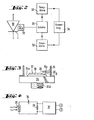
- FIG. 1 shows in cross section the semiconductor body of a thyristor to be monitored with a control element directly attached to it.
- FIG. 2 schematically shows the semiconductor arrangement according to the invention and a circuit arrangement suitable for evaluating the function of the control element.
- FIG. 3 shows partly in cross section and partly in side view the structure of a semiconductor component with parts of its housing and with a control element thermally attached to the housing.
- FIG. 4 schematically shows a photoresistor connected to a monitoring circuit, which is to be fastened in a corresponding manner to a semiconductor component.
- the semiconductor body 10 according to FIG. 1 forming a thyristor structure consists of a high-resistance, n-conducting central zone 1, of a higher-doped p-conducting zone 2 or 3 adjacent to each side thereof, and of a highly doped, n introduced into the upper zone conductive zone 5, and from the outer zones 2 and 5 applied contact electrodes 4 and 7 for the load current connection and from the p-conductive zone 3 applied control electrode 6 for the control connection.
- This layer structure is fixed between conductor parts 15 and 17.
- the semiconductor body 10 has an opening 8 which extends from a surface, for example from the contact electrode 7, into the p-type zone 3 and serves as a radiation window for the recombination radiation which arises in the semiconductor body when current flows. Because of the tendency of highly doped semiconductor material to absorb the recombination radiation, it is not sufficient to only to expose the semiconductor surface for producing a radiation surface, but an opening with a depth into one of the higher-resistance zones is required.
- the cross section of the opening 8 is adapted to the exposure surface of the control element provided.
- the position of the opening 8 is essentially arbitrary. For technological reasons, however, it is preferably located on the edge of the area determined by the contact electrode 7, for example in a cutout in the current conductor 17. In principle, the recombination radiation must emerge from the semiconductor material and strike the surface of the control element to be exposed. Accordingly, the control element with the surface section provided for the exposure is also attached in a corresponding manner to the semiconductor body.
- the control element is attached to the correspondingly prepared surface section of the semiconductor body 10 via an electrically insulating layer 20.
- Both the insulating material body 20 and the control element 30 can be attached, for example, by gluing or by soldering.
- an insulating body e.g. serve an adapted annular disc made of oxide ceramic, which is connected at its surfaces to the adjacent components and has a recess in its central area for the passage of the radiation onto the surface of the monitoring element to be exposed.
- a disk made of quartz can also be provided as the insulating material body 20, since quartz is completely permeable to the recombination radiation.
- Another possibility is to provide a corresponding socket for the arrangement of the control element 30, . Which can be attached to the insulating body 20 in the desired manner, and in which the control element is held.
- the entire exposed surface of the opening 8 can be provided with a layer of the oxide of the semiconductor material as a protective coating.
- the opening 8 can be produced by etching or by other known ablation processes.
- the control element 30 is thermally coupled to the semiconductor body 10 as described. This optimally allows both the current monitoring in the semiconductor component and the monitoring of the operating temperature thereof, which can increase undesirably, for example, due to failure of the cooling of the semiconductor component or due to deterioration in heat transfer in the structure of the latter.
- control elements without a pn junction, i.e. so-called photoresistors, and those based on semiconductors with at least one pn junction, i.e. Photodiodes and phototransistors are provided.
- the recombination radiation in the semiconductor body is proportional to the current flow through it over a wide range.
- the invention advantageously makes use of this fact, as well as the fact that control elements with a pn junction, the transmission behavior thereof and their dark current and, in the case of photoresistors, their dark resistance can be related to the operating temperature of the control element and thus also of the semiconductor component to be monitored.
- it is surprisingly easy to achieve essentially performance-free, inertia-free and phase-accurate monitoring of parameters in semiconductor components.
- a photodiode 30 is connected via a switch 31 on the one hand to a measuring circuit 32 for determining the forward voltage drop of the photodiode and on the other hand to a measuring circuit 33 for measuring the photocurrent.
- the switch can preferably be switched over with the help of a grid-synchronous clock generator in time with the grid frequency half-waves.
- a constant forward current of the latter is impressed by a current generator in the measuring circuit 32 of the photodiode 30, and the forward voltage drop of the photodiode is determined as a function of the thermal coupling of the photodiode to the component to be protected. This changes inversely proportional to the ambient temperature, so that a direct comparison of the measured values with the operating temperature to be monitored is possible.
- the photodiode 30 is acted on in the reverse direction with the aid of a voltage source in the measuring circuit 33, and the photocurrent is represented as a function of the illuminance on the exposed surface of the control element.
- the circuits as such. And the measures for measuring electrical quantities of the control element 30 and if necessary to reinforce the same are well known and not the subject of the invention.
- the dark current can also be represented as a function of the ambient temperature, it is possible to carry out temperature monitoring with the aid of the dark current in view of the usability of the control elements provided, even at high frequencies.
- a suitable error message can also be connected, for example, and a signal for an ignition lock can also be given for the ignition circuit of the component to be monitored, if it is a thyristor.
- the measurement results can thus be evaluated in a manner known per se and known from electronics.
- the block circuit shown in Figure 2 is not limited to the connection with only one control element. Rather, for a semiconductor rectifier circuit with six rectifier components, for example, all six control elements can be connected to the monitoring circuit shown.
- FIG. 1 Another possibility for the attachment of a control element is shown in FIG.
- the latter is provided with an opening 8.
- the control element 30 is attached via an insulating body 20 to a holding device 15 a in such a way that the recombination radiation emerging from the opening 8 of the semiconductor body 10 hits the surface of each control element to be exposed. It goes without saying that the assembly of such an arrangement requires special identifications of the housing parts for their position of certain mutual spatial assignment to ensure the functionality of the control element.
- the bracket 15 a is preferably made of a good heat-conducting metal for optimal thermal coupling of the control element to the housing 15 and is mounted so that the control element is as close as possible to the semiconductor body 10.
- control element 30 can also be attached at a suitable location on the base body 24.
- the connecting lines of the control element can be inserted through the housing at the top, for example with the aid of a ceramic tube.
- a photoresistor 30 is exposed to radiation of the semiconductor body, which is indicated only by arrows.
- the so-called light resistance of the control element 30 is a function of the illuminance.
- a base voltage is impressed on the photoresistor 30 from a battery 35 in the base circuit.
- the photocurrent generated by radiation in the photoresistor produces a change in resistance, which is evaluated with the aid of the voltage drop across the measuring resistor 36 and the circuit 37, which is not essential to the invention, which is connected in parallel with this.
- the dark resistance of the control element 30 can also serve as a function of the operating temperature of the latter and that of the semiconductor component for monitoring it.
- the semiconductor body 10 is first attached in a manner known per se to the pretreated carrier body 24 and the upper connecting conductor thereon, only a part of which is indicated by the component 17.
- the holding device 15 a carrying the control element 30 can be firmly connected to the upper housing part 15, for example by soldering or welding or with the aid of a metal adhesive.
- the housing upper part 15 is then attached to the carrier body 24 with the aid of a suitable marking.
- the advantage of the subject matter of the invention is an essentially powerless and inertia-free, phase-accurate and frequency-independent monitoring of parameters in semiconductor components by using known components with a photoelectric effect.
Abstract
Zur in jedem Falle sicheren und schnell ansprechenden Kontrolle des Betriebsverhaltens von Halbleiterbauelementen einer Halbleiteranordnung (10) ist als Kontrollelement (30) ein Bauelement mit innerem photoelektrischen Effekt zur Aufnahme der Rekombinationsstrahlung vorgesehen, die beim Stromdurchgang durch das Halbleiterbauelement (10) und dessen Halbleitermaterial entsteht. Dabei kann das Kontrollelement (30) gleichzeitig zur Überwachung des Laststromes und der Betriebstemperatur dienen. Es sind Kontrollelemente (30) auf Halbleiterbasis mit oder ohne pn-Übergang geeignet.To ensure that the operating behavior of semiconductor components of a semiconductor arrangement (10) is reliably and quickly responded to, a control element (30) is provided with a component with an internal photoelectric effect for receiving the recombination radiation that arises when current passes through the semiconductor component (10) and its semiconductor material. The control element (30) can simultaneously serve to monitor the load current and the operating temperature. Control elements (30) based on semiconductors with or without pn junction are suitable.
Description
Die Erfindung betrifft eine Halbleiteranordnung mit wennigstens einem Halbleiterbauelement und mit einem dessen Funktion überwachenden Kontrollelement.The invention relates to a semiconductor arrangement with at least one semiconductor component and with a control element monitoring its function.
Um eine unzulässige Überlastung von Halbleiterbauelementen hoher Strombelastbarkeit im Betrieb zu vermeiden, müssen die Betriebskenngrößen, insbesondere der Laststrom und die Temperatur, überwacht werden. Beispielsweise werden als thermische Sensoren Bimetallschalter oder PPC-Widerstände oder NTC-Widerstände verwendet, die am Halbleiterbauelement befestigt sind und bei Erreichen einer maximal zulässigen Betriebstemperatur des letzteren dessen Abschaltung bewirkt. Derartige Kontrollelemente können jedoch nicht unmittelbar am Halbleiterkörper der Bauelemente angebracht werden. Infolge der zwischen dem Halbleiterkörper und dem Kontrollelement vorhandenen Wärmewiderstände entsteht eine Ansprechverzögerung, welche häufig einen wirksamen Schutz der Halbleiterbauelemente durch.solche thermischen Sensoren verhindert.In order to avoid inadmissible overloading of semiconductor components with a high current carrying capacity during operation, the operating parameters, in particular the load current and the temperature, must be monitored. For example, bimetallic switches or PPC resistors or NTC resistors are used as thermal sensors, which are attached to the semiconductor component and cause the latter to be switched off when the maximum permissible operating temperature of the latter is reached. However, such control elements cannot be attached directly to the semiconductor body of the components. As a result of the thermal resistances present between the semiconductor body and the control element, there is a delay in response, which often prevents effective protection of the semiconductor components by such thermal sensors.
Bekannt ist weiterhin auch die Verwendung von speziellen Halbleitersensoren. Ihr Einsatz bringt jedoch zusätzliche Spannungs- und Wärmeverluste mit sich und erfordert einen teilweise bedeutenden zusätzlichen Platzbedarf.The use of special semiconductor sensors is also known. However, their use entails additional voltage and heat losses and requires a significant additional space.
Bei entsprechenden Überlastfällen werden die relativ teueren Sicherungselemente dennoch zerstört, und schließlich sind dieselben nicht in allen Fällen zuverlässig. Der Erfindung lag daher die Aufgabe zugrunde, eine Überwachungseinrichtung für Halbleiterbauelemente anzugeben, welche eine in jedem Falle sichere und möglichst schnell ansprechende Kontrolle des elektrischen bzw. thermischen Betriebsverhaltens von Halbleiterbauelementen ermöglicht. Die Erfindungg eht von der Erkenntnis aus, daß beim Stromfluß durch einen Halbleiterkörper in diesem eine sogenannte Rekombinationsstrahlung entsteht, daß es sich bei dieser Strahlung um eine Infrarotstrahlung handelt, und daß diese Infrarotstrahlung dem Stromfluß proportional ist.In the event of corresponding overloads, the relatively expensive fuse elements are nevertheless destroyed, and ultimately they are not reliable in all cases. The invention was therefore based on the object of specifying a monitoring device for semiconductor components which in any case enables the electrical or thermal operating behavior of semiconductor components to be checked reliably and as quickly as possible. The invention is based on the knowledge that when current flows through a semiconductor body, so-called recombination radiation arises, that this radiation is infrared radiation, and that this infrared radiation is proportional to the current flow.
Die Lösung dieser Aufgabe besteht bei einer Halbleiteranordnung der eingangs erwähnten Art darin, daß sie als Kontrollelement ein Bauelement mit innerem photoelektrischen Effekt zur Aufnahme der beim Stromdurchgang durch das Halbleiterbauelement in dessen Halbleitermaterial entstehenden Rekombinationsstrahlung aufweist.The solution to this problem in a semiconductor arrangement of the type mentioned at the outset is that, as a control element, it has a component with an internal photoelectric effect for receiving the recombination radiation which arises in the semiconductor material when the current passes through the semiconductor component.
Das Kontrollelement ist gleichzeitig zur Überwachung des Laststroms und d'er Temperatur des Halbleiterbauelements vorgesehen.The control element is provided at the same time for monitoring the load current and the temperature of the semiconductor component.
Es können Kontrollelemente auf Halbleiterbasis sowohl mit wenigstens einem pn-übergang und zur Temperaturüberwachung mit Hilfe ihres Durchlaßverhaltens oder mit Hilfe ihres Dunkelstromverhaltens, oder aber Kontrollelemente auf Halbleiterbasis ohne pn-übergang und zur Temperaturüberwachung mit Hilfe ihrer Dunkelwiderstandsänderung, jeweils in der Sperrphase des Halbleiterbauelements, vorgesehen sein. Anhand der in den Figuren 1 - 4 dargestellten Ausführungsbeispiele wird der Gegenstand der Erfindung aufgezeigt und erläutert.It can transition pn control elements based on semiconductors both with transition pn least one, and for temperature monitoring with the aid of their D urchlaßverhaltens or with the aid of its dark-current behavior, or control elements on semiconductor basis without and for temperature monitoring with the aid of its dark resistance change in each case in the blocking phase of the semiconductor component, be provided. The subject matter of the invention is shown and explained on the basis of the exemplary embodiments illustrated in FIGS. 1-4.
Figur 1 zeigt im Querschnitt den Halbleiterkörper eines zu überwachenden Thyristors mit einem unmittelbar daran befestigten Kontrollelement. In Figur 2 ist schematisch die Halbleiteranordnung nach der Erfindung und eine zur Auswertung der Funktion des Kontrollelements geeignete Schaltungsanordnung dargestellt. Figur 3 zeigt teilweise im Querschnitt und teilweise in Seitenansicht den Aufbau eines Halbleiterbauelements mit Teilen seines Gehäuses und mit einem thermisch am Gehäuse befestigten Kontrollelement. In Figur 4 ist schematisch ein mit einer überwachungsschaltung verbundener Photowiderstand gezeigt, der in entsprechender Weise an einem Halbleiterbauelement zu befestigen ist.Figure 1 shows in cross section the semiconductor body of a thyristor to be monitored with a control element directly attached to it. FIG. 2 schematically shows the semiconductor arrangement according to the invention and a circuit arrangement suitable for evaluating the function of the control element. FIG. 3 shows partly in cross section and partly in side view the structure of a semiconductor component with parts of its housing and with a control element thermally attached to the housing. FIG. 4 schematically shows a photoresistor connected to a monitoring circuit, which is to be fastened in a corresponding manner to a semiconductor component.
Gleiche Teile sind in allen Figuren mit gleichen Bezeichnungen versehen.Identical parts are given the same designations in all figures.
Der eine Thyristorstruktur bildende Halbleiterkörper 10 nach Figur 1 besteht aus einer hochohmigen, n-leitenden Mittelzone 1, aus je einer an jeder Seite derselben angrenzenden, höherdotierten p-leitenden Zone 2 bzw. 3, aus einer in die obere Zone eingebrachten, hochdotierten, n-leitenden Zone 5, sowie aus auf die äußeren Zonen 2 bzw. 5 aufgebrachten Kontaktelektroden 4 bzw. 7 für den Laststromanschluß und aus einer auf die p-leitende Zone 3 aufgebrachten Steuerelektrode 6 für den Steueranschluß. Dieser Schichtenaufbau ist zwischen Leiterteilen 15 bzw. 17 fest angeordnet.The
Erfindungsgemäß weist der Halbleiterkörper 10 eine von einer Oberfläche, beispielsweise von der Kontaktelektrode 7, sich bis in die p-leitende Zone 3 erstreckende Öffnung 8 auf, die als Strahlungsfenster für die im Halbleiterkörper bei Stromfluß entstehende Rekombinationsstrahlung dient. Wegen der Neigung von hochdotiertem Halbleitermaterial zur Absorption der Rekombinationsstrahlung genügt es nicht, lediglich die Halbleiteroberfläche zur Herstellung einer Strahlungsfläche freizulegen, sondern es ist eine Öffnung mit einer Tiefe bis in eine der höherohmigen Zonen erforderlich. Der Querschnitt der öffnung 8 ist der Belichtungsfläche des vorgesehenen Kontrollelements angepaßt. Die Lage der öffnung 8 ist im wesentlichen beliebig. Aus technologischen Gründen befindet sie sich jedoch vorzugsweise am Rande der durch die Kontaktelektrode 7 bestimmten Fläche, beispielsweise in einer Aussparung des Stromleiters 17. Grundsätzlich muß die Rekombinationsstrahlung aus dem Halbleitermaterial austreten und auf die zu belichtende Fläche des Kontrollelements auftreffen. Demzufolge ist auch das Kontrollelement mit dem für die Belichtung vorgesehenen Flächenabschnitt in entsprechender Weise auf dem Halbleiterkörper angebracht.According to the invention, the
Gemäß der Darstellung in Figur 1 ist das Kontrollelement über eine elektrisch isolierende Schicht 20 auf dem entsprechend vorbereiteten Oberflächenabschnitt des Halbleiterkörpers 10 befestigt. Die Befestigung sowohl des Isolierstoffkörpers 20 als auch des Kontrollelements 30 kann beispielsweise.durch Kleben oder auch durch Löten erfolgen. Als Isolierstoffkörper kann z.B. eine angepaßt ringförmige Scheibe aus Oxidkeramik dienen, die an ihren Flächen mit den angrenzenden Bauteilen verbunden ist und in ihrem zentralen Bereich eine Aussparung aufweist zum Durchtritt der Strahlung auf die zu belichtende Fläche des Überwachungselements.According to the illustration in FIG. 1, the control element is attached to the correspondingly prepared surface section of the
Als Isolierstoffkörper 20 kann jedoch auch eine Scheibe aus Quarz vorgesehen sein, da Quarz für die Rekombinationsstrahlung uneingeschränkt durchlässig ist.However, a disk made of quartz can also be provided as the
Eine andere Möglichkeit besteht darin, für die Anordnung des Kontrollelements 30 eine entsprechende Fassung vorzusehen, .die auf dem Isolierstoffkörper 20 in gewünschter Weise befestigt werden kann, und in welcher das Kontrollelement gehaltert ist.Another possibility is to provide a corresponding socket for the arrangement of the
Die gesamte freiliegende Fläche der öffnung 8 kann mit einer Schicht aus dem Oxid des Halbleitermaterials als schützendem Überzug versehen sein.The entire exposed surface of the
Die Herstellung der Öffnung 8 kann durch Ätzen oder durch andere bekannte abtragende Verfahren erfolgen. Das Kontrollelement 30 ist wie beschrieben thermisch mit dem Halbleiterkörper 10 gekoppelt. Das gestattet optimal sowohl die Stromüberwachung im Halbleiterbauelement als auch die Überwachung der Betriebstemperatur desselben, die beispielsweise durch Ausfall der Kühlung des Halbleiterbauelements oder aber durch Verschlechterung eines Wärmeübergangs im Aufbau desselben in unerwünschter Weise zunehmen kann.The opening 8 can be produced by etching or by other known ablation processes. The
Es sind Kontrollelemente auf Halbleiterbasis ohne pn-Übergang, d.h. sogenannte Photowiderstände, und solche auf Halbleiterbasis mit wenigstens einem pn-Ubergang, d.h. Photodioden und Phototransistoren vorgesehen. Wie bereits oben ausgeführt, ist die Rekombinationsstrahlung im Halbleiterkörper dem Stromfluß durch denselben in weiten Bereichen proportional. Von dieser Tatsache, sowie davon, daß bei Kontrollelementen mit pn-übergang das Durchlaßverhalten derselben sowie ihr Dunkelstrom und bei Photowiderständen deren Dunkelwiderstand jeweils zur Betriebstemperatur des Kontrollelements und damit auch des zu überwachenden Halbleiterbauelements in Beziehung gesetzt werden kann, macht die Erfindung in vorteilhafterweise Gebrauch. Dadurch ist überraschend einfach eine im wesentlichen leistungs- und trägheitslose sowie phasentreue Überwachung von Kenngrößen bei Halbleiterbauelementen erzielbar.They are semiconductor-based control elements without a pn junction, i.e. so-called photoresistors, and those based on semiconductors with at least one pn junction, i.e. Photodiodes and phototransistors are provided. As already explained above, the recombination radiation in the semiconductor body is proportional to the current flow through it over a wide range. The invention advantageously makes use of this fact, as well as the fact that control elements with a pn junction, the transmission behavior thereof and their dark current and, in the case of photoresistors, their dark resistance can be related to the operating temperature of the control element and thus also of the semiconductor component to be monitored. As a result, it is surprisingly easy to achieve essentially performance-free, inertia-free and phase-accurate monitoring of parameters in semiconductor components.
Aus Figur 2 ist zu erkennen, daß beispielsweise eine Photodiode 30 über einen Schalter 31 einerseits mit einem Meßkreis 32 zur Feststellung des Durchlaßspannungsabfalls der Photodiode und andererseits mit einem Meßkreis 33 zur Messung des Photostromes verbunden ist. Dabei ist der Schalter vorzugsweise mit Hilfe eines netzsynchronen Taktgenerators im Takt der Netzfrequenzhalbwellen umschaltbar. Einmal wird durch einen Stromgenerator im Meßkreis 32 der Photodiode 30 ein konstanter Durchlaßstrom der letzteren eingeprägt, und in Abhängigkeit von der thermischen Kopplung der Photodiode an das zu schützende Bauelement wird der Durchlaßspannungsabfall der Photodiode festgestellt. Dieser verändert sich umgekehrt proportional zur Umgebungstemperatur, so daß ein direkter Vergleich der gemessenen Werte mit der zu überwachenden Betriebstemperatur möglich ist.It can be seen from FIG. 2 that, for example, a
Zum anderen wird die Photodiode 30 mit Hilfe einer Spannungsquelle im Meßkreis 33-in Sperrichtung beaufschlagt, und der Photostrom stellt sich als Funktion der Beleuchtungsstärke auf der belichteten Fläche des Kontrollelementes dar. Die Schaltkreise als solche .sowie die Maßnahmen zur Messung von elektrischen Größen des Kontrollelementes 30 und bedarfsweise zur Verstärkung derselben sind hinlänglich bekannt und nicht Gegenstand der Erfindung.On the other hand, the
Nachdem der Dunkelstrom ebenfalls als Funktion der Umgebungstemperatur darstellbar ist, ist es möglich, im Hinblick auf die Verwendbarkeit der vorgesehenen Kontrollelemente auch bei hohen Frequenzen die Temperaturüberwachung mit Hilfe des Dunkelstromes vorzunehmen. Im Zusammenhang mit der Ermittlung von Meßwerten kann beispielsweise auch eine geeignete Fehlermeldung mit verbunden sein, ferner kann für den Zündkreis des zu überwachenden Bauelements, wenn es sich um einen Thyristor handelt, auch ein Signal für eine Zündsperre erfolgen.Since the dark current can also be represented as a function of the ambient temperature, it is possible to carry out temperature monitoring with the aid of the dark current in view of the usability of the control elements provided, even at high frequencies. In connection with the determination of measured values, a suitable error message can also be connected, for example, and a signal for an ignition lock can also be given for the ignition circuit of the component to be monitored, if it is a thyristor.
Die Auswertung der Meßergebnisse ist somit in an sich bekannter und aus der Elektronik bekannter Weise durchführbar.The measurement results can thus be evaluated in a manner known per se and known from electronics.
Die in Figur 2 dargestellte Blockschaltung ist nicht auf die Verbindung mit nur einem Kontrollelement beschränkt. Vielmehr lassen sich beispielsweise für eine Halbleitergleichrichterschaltung mit sechs Gleichrichterbauelementen sämtliche sechs Kontrollelemente mit der einen dargestellten überwachungsschaltung verbinden.The block circuit shown in Figure 2 is not limited to the connection with only one control element. Rather, for a semiconductor rectifier circuit with six rectifier components, for example, all six control elements can be connected to the monitoring circuit shown.
In Figur 3 ist eine andere Möglichkeit für die Anbringung eines Kontrollelements dargestellt. Ein vorzugsweise aus Kupfer bestehender Trägerkörper 24, der gleichzeitig als Stromleiter und als Gehäuseunterteil mit einem Schraubstutzen 24 b dient, weist an seiner oberen Fläche einen Ansatz 24 a zur Anbringung des Halbleiterkörpers 10 auf. Der letztere ist mit einer Öffnung 8 versehen. An der Innenfläche des nur teilweise dargestellten Gehäuseoberteiles 15 ist das Kontrollelement 30 über einen Isolierstoffkörper 20 an einer Haltevorrichtung 15 a so angebracht, daß die aus der Öffnung 8 des Halbleiterkörpers 10 austretende Rekombinationsstrahlung die zu belichtende Fläche jedes Kontrollelements trifft. Es versteht sich, daß der Zusammenbau einer solchen Anordnung besondere Kennzeichnungen der Gehäuseteile zu deren Lage bestimmter gegenseitiger räumlicher Zuordnung zur Sicherstellung der Fuhktionsfähigkeit des Kontrollelements erfordert.Another possibility for the attachment of a control element is shown in FIG. A
Die Halterung 15 a besteht vorzugsweise aus einem gut wärmeleitenden Metall zur optimalen thermischen Ankopplung des Kontrollelements an das Gehäuse 15 und ist so angebracht, daß ein möglichst geringer Abstand des Kontrollelements zum Halbleiterkörper 10 besteht.The
Eine solche thermische Kopplung bringt wohl gegenüber der unmittelbaren Verbindung mit dem Halbleiterkörper wegen des längeren Weges der Verlustwärme zum Kontrollelement eine gewisse Trägheit der Uberwachungsfunktion mit sich, erscheint jedoch besonders vorteilhaft zur Überwachung der Wärmewiderstände im Aufbau-des zu überwachenden Bauelements bzw. der Funktion der Kühleinrichtung. Selbstverständlich kann die Befestigung des Kontrollelementes 30 auch an geeigneter Stelle des Grundkörpers 24 erfolgen.Compared to the direct connection to the semiconductor body, such a thermal coupling probably entails a certain inertia of the monitoring function due to the longer path of the heat loss to the control element, but appears to be particularly advantageous for monitoring the thermal resistance in the structure of the component to be monitored or the function of the cooling device . Of course, the
Die Anschlußleitungen des Kontrollelements können beispielsweise mit Hilfe eines Keramikrohres durch das Gehäuse oben eingeführt sein.The connecting lines of the control element can be inserted through the housing at the top, for example with the aid of a ceramic tube.
Nach der Darstellung in Figur 4 ist ein Photowiderstand 30 einer lediglich durch Pfeile symbolisiert angedeuteten Strahlung des Halbleiterkörpers ausgesetzt. Entsprechend dem Zusammenhang zwischen Photostrom und Beleuchtungsstärke z. B. bei einer Photodiode ist der sogenannte helle Widerstand des Kontrollelements 30 eine Funktion der Beleuchtungsstärke.According to the illustration in FIG. 4, a
In dem Basiskreis ist dem Photowiderstand 30 aus einer Batterie 35 eine Basisspannung eingeprägt. Der durch Bestrahlung erzeugte Photostrom im Photowiderstand erzeugt eine Widerstandsänderung, die mit Hilfe des Spannungsabfalls an den Meßwiderstand 36 und der zu diesem parallel geschalteten nicht erfindungswesentlichen Schaltung 37 ausgewertet wird. Im wesentlichen mit derselben Grundschaltung kann auch der Dunkelwiderstand des Kontrollelements 30 als Funktion der Betriebstemperatur des letzteren und des zum Halbleiterbauelementes zu dessen Überwachung dienen.A base voltage is impressed on the photoresistor 30 from a
Bei der Herstellung eines Aufbaus gemäß Figur 3 werden in an sich bekannter Weise zunächst auf dem vorbehandelten Trägerkörper 24 der Halbleiterkörper 10 und auf diesem der obere Anschlußleiter angebracht, wovon mit dem Bauteil 17 nur ein Teil desselben angedeutet ist.In the manufacture of a structure according to FIG. 3, the
Die das Kontrollelement 30 tragende Haltevorrichtung 15 a kann mit dem Gehäuseoberteil 15 beispielsweise durch Löten oder Schweißen oder mit Hilfe eines Metallklebers fest verbunden sein. Mit Hilfe einer geeigneten Markierung wird anschließend das Gehäuseoberteil 15 auf dem Trägerkörper 24 befestigt.The holding
Der Vorteil des Gegenstandes der Erfindung besteht in einer im wesentlichen leistungs- und trägheitslosen sowie phasentreuen und frequenzunabhängigen Überwachung von Kenngrößen bei Halbleiterbauelementen durch Anwendung bekannter Bauelemente mit photoelektrischem Effekt.The advantage of the subject matter of the invention is an essentially powerless and inertia-free, phase-accurate and frequency-independent monitoring of parameters in semiconductor components by using known components with a photoelectric effect.
Claims (5)
daß als Kontrollelement ein Bauelement mit innerem photoelektrischen Effekt zur Aufnahme der beim Stromdurchgang durch das Halbleiterbauelement in dessen Halbleitermaterial entstehenden Rekombinationsstrahlung vorgesehen ist.1. Semiconductor arrangement with at least one semiconductor component and with a control element monitoring its function, characterized in that
that a component with an internal photoelectric effect is provided as a control element for receiving the recombination radiation generated in the semiconductor material when the current passes through the semiconductor component.
daß das Kontrollelement zur Strom- und Temperaturüberwachung des Halbleiterbauelements vorgesehen ist.2. Semiconductor arrangement according to claim 1, characterized in that
that the control element is provided for current and temperature monitoring of the semiconductor component.
daß ein Kontrollelement auf Halbleiterbasis mit wenigstens einem pn-übergang und zur Temperaturüberwachungmit Hilfe seines Durchlaßverhaltens in der Sperrphase des Halbleiterbauelements vorgesehen ist.3. Semiconductor arrangement according to claim 2, characterized in that
that a control element on a semiconductor basis with at least one pn junction and for temperature monitoring by means of its transmission behavior is provided in the blocking phase of the semiconductor component.
daß ein Kontrollelement auf Halbleiterbasis mit wenigstens einem pn-Übergang und zur Temperaturüberwachung mit Hilfe seines Dunkelstromverhaltens in der Sperrphase des Halbleiterbauelements vorgesehen ist.4. Semiconductor arrangement according to claim 2, characterized in that
that a control element on a semiconductor basis with at least one pn junction and for temperature monitoring with the aid of its dark current behavior is provided in the blocking phase of the semiconductor component.
daß ein Kontrollelement auf Halbleiterbasis ohne pn-Übergang und zur Temperaturüberwachung mit Hilfe seiner Dunkelwiderstandsänderung in der Sperrphase des Halbleiterbauelements vorgesehen ist.5. Semiconductor arrangement according to claim 2, characterized in
that a control element on a semiconductor basis without pn junction and for temperature monitoring with the help of its dark resistance change is provided in the blocking phase of the semiconductor component.
Applications Claiming Priority (2)
| Application Number | Priority Date | Filing Date | Title |
|---|---|---|---|
| DE3009192A DE3009192C2 (en) | 1980-03-11 | 1980-03-11 | Overload protection arrangement |
| DE3009192 | 1980-03-11 |
Publications (2)
| Publication Number | Publication Date |
|---|---|
| EP0035767A1 true EP0035767A1 (en) | 1981-09-16 |
| EP0035767B1 EP0035767B1 (en) | 1986-06-18 |
Family
ID=6096791
Family Applications (1)
| Application Number | Title | Priority Date | Filing Date |
|---|---|---|---|
| EP81101619A Expired EP0035767B1 (en) | 1980-03-11 | 1981-03-06 | Semiconductor device |
Country Status (4)
| Country | Link |
|---|---|
| US (1) | US4744672A (en) |
| EP (1) | EP0035767B1 (en) |
| JP (1) | JPS56142668A (en) |
| DE (1) | DE3009192C2 (en) |
Cited By (1)
| Publication number | Priority date | Publication date | Assignee | Title |
|---|---|---|---|---|
| FR2686449A1 (en) * | 1992-01-17 | 1993-07-23 | Legrand Sa | Combined switch with mechanical switching means and static switching means |
Families Citing this family (19)
| Publication number | Priority date | Publication date | Assignee | Title |
|---|---|---|---|---|
| DE3415764A1 (en) * | 1984-04-27 | 1985-10-31 | Siemens AG, 1000 Berlin und 8000 München | Circuit arrangement for monitoring the temperature of integrated circuits |
| US5159564A (en) * | 1988-12-22 | 1992-10-27 | North Carolina State University | Thermal memory cell and thermal system evaluation |
| US5021981A (en) * | 1988-12-22 | 1991-06-04 | North Carolina State University | Thermal memory cell and thermal system evaluation |
| GB9026034D0 (en) * | 1990-11-29 | 1991-01-16 | Rolls Royce Plc | A fluid temperature measuring device |
| US5154514A (en) * | 1991-08-29 | 1992-10-13 | International Business Machines Corporation | On-chip temperature sensor utilizing a Schottky barrier diode structure |
| US7140766B2 (en) * | 1999-08-04 | 2006-11-28 | Given Imaging Ltd. | Device, system and method for temperature sensing in an in-vivo device |
| IL131242A0 (en) * | 1999-08-04 | 2001-01-28 | Given Imaging Ltd | A method for temperature sensing |
| US20040019459A1 (en) * | 2002-07-29 | 2004-01-29 | Paul Dietz | Auto-characterization of optical devices |
| US6974973B2 (en) * | 2002-11-08 | 2005-12-13 | Micron Technology, Inc. | Apparatus for determining temperature of an active pixel imager and correcting temperature induced variations in an imager |
| WO2004112567A2 (en) * | 2003-06-26 | 2004-12-29 | Given Imaging Ltd. | Methods, device and system for in vivo detection |
| US9578724B1 (en) | 2013-08-20 | 2017-02-21 | Ketra, Inc. | Illumination device and method for avoiding flicker |
| USRE48956E1 (en) | 2013-08-20 | 2022-03-01 | Lutron Technology Company Llc | Interference-resistant compensation for illumination devices using multiple series of measurement intervals |
| US9769899B2 (en) * | 2014-06-25 | 2017-09-19 | Ketra, Inc. | Illumination device and age compensation method |
| USRE48955E1 (en) | 2013-08-20 | 2022-03-01 | Lutron Technology Company Llc | Interference-resistant compensation for illumination devices having multiple emitter modules |
| US9557214B2 (en) | 2014-06-25 | 2017-01-31 | Ketra, Inc. | Illumination device and method for calibrating an illumination device over changes in temperature, drive current, and time |
| US9736903B2 (en) * | 2014-06-25 | 2017-08-15 | Ketra, Inc. | Illumination device and method for calibrating and controlling an illumination device comprising a phosphor converted LED |
| US9392660B2 (en) | 2014-08-28 | 2016-07-12 | Ketra, Inc. | LED illumination device and calibration method for accurately characterizing the emission LEDs and photodetector(s) included within the LED illumination device |
| US9510416B2 (en) | 2014-08-28 | 2016-11-29 | Ketra, Inc. | LED illumination device and method for accurately controlling the intensity and color point of the illumination device over time |
| US11272599B1 (en) | 2018-06-22 | 2022-03-08 | Lutron Technology Company Llc | Calibration procedure for a light-emitting diode light source |
Citations (1)
| Publication number | Priority date | Publication date | Assignee | Title |
|---|---|---|---|---|
| DE2740539A1 (en) * | 1976-09-22 | 1978-03-23 | Cutler Hammer World Trade Inc | SEMI-CONDUCTOR DEVICE WITH POWER AND TEMPERATURE SWITCH |
Family Cites Families (15)
| Publication number | Priority date | Publication date | Assignee | Title |
|---|---|---|---|---|
| US2504628A (en) * | 1946-03-23 | 1950-04-18 | Purdue Research Foundation | Electrical device with germanium alloys |
| US3102201A (en) * | 1958-12-15 | 1963-08-27 | Rca Corp | Semiconductor device for generating modulated radiation |
| US3026469A (en) * | 1959-11-13 | 1962-03-20 | Avco Corp | Voltage regulator and overload protection system |
| NL260956A (en) * | 1961-02-07 | |||
| NL299168A (en) * | 1962-10-15 | |||
| DE1238506B (en) * | 1963-03-14 | 1967-04-13 | Philips Nv | Arrangement for amplifying broadband electrical signals |
| US3303431A (en) * | 1964-02-10 | 1967-02-07 | Ibm | Coupled semiconductor injection laser devices |
| US3301716A (en) * | 1964-09-10 | 1967-01-31 | Rca Corp | Semiconductor device fabrication |
| GB1112411A (en) * | 1965-01-21 | 1968-05-08 | Mullard Ltd | Improvements in and relating to semiconductor devices |
| DE1489518A1 (en) * | 1965-07-07 | 1969-04-03 | Siemens Ag | Light-emitting diode and process for their manufacture |
| US3398311A (en) * | 1965-12-29 | 1968-08-20 | Westinghouse Electric Corp | Electroluminescent device |
| US3575645A (en) * | 1969-07-17 | 1971-04-20 | Gen Motors Corp | Power zener package |
| US3622849A (en) * | 1970-06-23 | 1971-11-23 | Gen Electric | Thyristor junction temperature monitor |
| US4125777A (en) * | 1977-08-17 | 1978-11-14 | Rca Corporation | Radiation emitter-detector package |
| DE2755081A1 (en) * | 1977-12-10 | 1979-06-13 | Ristow Kg Dr Alfred | Transistor overload protection system - has inversely operated diode which controls transistor input voltage, and is thermally connected to it |
-
1980
- 1980-03-11 DE DE3009192A patent/DE3009192C2/en not_active Expired
-
1981
- 1981-03-06 EP EP81101619A patent/EP0035767B1/en not_active Expired
- 1981-03-10 JP JP3323981A patent/JPS56142668A/en active Granted
- 1981-03-10 US US06/242,251 patent/US4744672A/en not_active Expired - Fee Related
Patent Citations (1)
| Publication number | Priority date | Publication date | Assignee | Title |
|---|---|---|---|---|
| DE2740539A1 (en) * | 1976-09-22 | 1978-03-23 | Cutler Hammer World Trade Inc | SEMI-CONDUCTOR DEVICE WITH POWER AND TEMPERATURE SWITCH |
Cited By (1)
| Publication number | Priority date | Publication date | Assignee | Title |
|---|---|---|---|---|
| FR2686449A1 (en) * | 1992-01-17 | 1993-07-23 | Legrand Sa | Combined switch with mechanical switching means and static switching means |
Also Published As
| Publication number | Publication date |
|---|---|
| DE3009192C2 (en) | 1984-05-10 |
| US4744672A (en) | 1988-05-17 |
| JPH026231B2 (en) | 1990-02-08 |
| JPS56142668A (en) | 1981-11-07 |
| EP0035767B1 (en) | 1986-06-18 |
| DE3009192A1 (en) | 1981-09-24 |
Similar Documents
| Publication | Publication Date | Title |
|---|---|---|
| EP0035767B1 (en) | Semiconductor device | |
| DE60030619T2 (en) | guard | |
| DE2619312A1 (en) | SEMI-CONDUCTOR HEATING ELEMENT | |
| DE2235783C2 (en) | Metal oxide varistor element | |
| DE69818011T2 (en) | ELECTRICAL MELTFUSE | |
| DE3338718C2 (en) | ||
| DE3725438A1 (en) | METHOD FOR PRODUCING A WIRED MICRO FUSE | |
| DE19519462C2 (en) | Heat generating electrical component | |
| DE2748567C2 (en) | Power semiconductor component | |
| DE3535923A1 (en) | SUBSTRATE CONSTRUCTION | |
| DE4036109A1 (en) | RESISTANCE TEMPERATURE SENSOR | |
| EP0809094A1 (en) | Method for making a sensor device for temperature measurement | |
| EP1459331A2 (en) | Spring clip, surge diverter with a spring slip and a surge diverter arrangement | |
| DE19848823A1 (en) | Thermistor with negative temperature coefficient for electrical and electronic machine | |
| DE8006555U1 (en) | Semiconductor device | |
| DE3390451C2 (en) | Laser laser process | |
| DE4343706B4 (en) | Heat sensitive capacitor | |
| DE102015214628A1 (en) | Heating device for a household appliance | |
| DE3040867A1 (en) | SEMICONDUCTOR ADDITION AND METHOD FOR THEIR PRODUCTION | |
| DE3245629A1 (en) | Fuse element with a thick-film resistor arrangement | |
| DE3221919C2 (en) | Monitoring element for power circuits | |
| DE3728489A1 (en) | Electrical fuse link | |
| DE4020577C3 (en) | Semiconductor arrangement with solder connection between semiconductor component, insulating plate and heat dissipation plate | |
| DE10011009B4 (en) | Thermistor with negative temperature coefficient | |
| DE1952221A1 (en) | MIS field effect transistor |
Legal Events
| Date | Code | Title | Description |
|---|---|---|---|
| PUAI | Public reference made under article 153(3) epc to a published international application that has entered the european phase |
Free format text: ORIGINAL CODE: 0009012 |
|
| AK | Designated contracting states |
Designated state(s): CH FR GB IT |
|
| 17P | Request for examination filed |
Effective date: 19820226 |
|
| GRAA | (expected) grant |
Free format text: ORIGINAL CODE: 0009210 |
|
| AK | Designated contracting states |
Kind code of ref document: B1 Designated state(s): CH FR GB IT LI |
|
| REG | Reference to a national code |
Ref country code: CH Ref legal event code: PFA Free format text: SEMIKRON ELEKTRONIK GMBH |
|
| ITF | It: translation for a ep patent filed |
Owner name: MODIANO & ASSOCIATI S.R.L. |
|
| ET | Fr: translation filed | ||
| RAP2 | Party data changed (patent owner data changed or rights of a patent transferred) |
Owner name: SEMIKRON ELEKTRONIK GMBH |
|
| PLBE | No opposition filed within time limit |
Free format text: ORIGINAL CODE: 0009261 |
|
| STAA | Information on the status of an ep patent application or granted ep patent |
Free format text: STATUS: NO OPPOSITION FILED WITHIN TIME LIMIT |
|
| 26N | No opposition filed | ||
| PGFP | Annual fee paid to national office [announced via postgrant information from national office to epo] |
Ref country code: CH Payment date: 19900309 Year of fee payment: 10 |
|
| PGFP | Annual fee paid to national office [announced via postgrant information from national office to epo] |
Ref country code: FR Payment date: 19900327 Year of fee payment: 10 |
|
| ITTA | It: last paid annual fee | ||
| PGFP | Annual fee paid to national office [announced via postgrant information from national office to epo] |
Ref country code: GB Payment date: 19900906 Year of fee payment: 10 |
|
| PG25 | Lapsed in a contracting state [announced via postgrant information from national office to epo] |
Ref country code: GB Effective date: 19910306 |
|
| PG25 | Lapsed in a contracting state [announced via postgrant information from national office to epo] |
Ref country code: LI Effective date: 19910331 Ref country code: CH Effective date: 19910331 |
|
| GBPC | Gb: european patent ceased through non-payment of renewal fee | ||
| PG25 | Lapsed in a contracting state [announced via postgrant information from national office to epo] |
Ref country code: FR Effective date: 19911129 |
|
| REG | Reference to a national code |
Ref country code: CH Ref legal event code: PL |
|
| REG | Reference to a national code |
Ref country code: FR Ref legal event code: ST |