EP0034973A1 - Dispositif de modulation numérique linéaire pour émetteur hertzien - Google Patents
Dispositif de modulation numérique linéaire pour émetteur hertzien Download PDFInfo
- Publication number
- EP0034973A1 EP0034973A1 EP81400228A EP81400228A EP0034973A1 EP 0034973 A1 EP0034973 A1 EP 0034973A1 EP 81400228 A EP81400228 A EP 81400228A EP 81400228 A EP81400228 A EP 81400228A EP 0034973 A1 EP0034973 A1 EP 0034973A1
- Authority
- EP
- European Patent Office
- Prior art keywords
- modulation
- modulator
- input
- mixer
- output
- Prior art date
- Legal status (The legal status is an assumption and is not a legal conclusion. Google has not performed a legal analysis and makes no representation as to the accuracy of the status listed.)
- Withdrawn
Links
Images

Classifications
-
- H—ELECTRICITY
- H04—ELECTRIC COMMUNICATION TECHNIQUE
- H04L—TRANSMISSION OF DIGITAL INFORMATION, e.g. TELEGRAPHIC COMMUNICATION
- H04L27/00—Modulated-carrier systems
- H04L27/18—Phase-modulated carrier systems, i.e. using phase-shift keying
- H04L27/20—Modulator circuits; Transmitter circuits
- H04L27/2032—Modulator circuits; Transmitter circuits for discrete phase modulation, e.g. in which the phase of the carrier is modulated in a nominally instantaneous manner
- H04L27/2053—Modulator circuits; Transmitter circuits for discrete phase modulation, e.g. in which the phase of the carrier is modulated in a nominally instantaneous manner using more than one carrier, e.g. carriers with different phases
- H04L27/206—Modulator circuits; Transmitter circuits for discrete phase modulation, e.g. in which the phase of the carrier is modulated in a nominally instantaneous manner using more than one carrier, e.g. carriers with different phases using a pair of orthogonal carriers, e.g. quadrature carriers
- H04L27/2067—Modulator circuits; Transmitter circuits for discrete phase modulation, e.g. in which the phase of the carrier is modulated in a nominally instantaneous manner using more than one carrier, e.g. carriers with different phases using a pair of orthogonal carriers, e.g. quadrature carriers with more than two phase states
- H04L27/2071—Modulator circuits; Transmitter circuits for discrete phase modulation, e.g. in which the phase of the carrier is modulated in a nominally instantaneous manner using more than one carrier, e.g. carriers with different phases using a pair of orthogonal carriers, e.g. quadrature carriers with more than two phase states in which the data are represented by the carrier phase, e.g. systems with differential coding
Definitions
- the invention relates to telecommunications systems transmitting digital information and more particularly relates to a "linear" digital modulation device (comprising a linear modulator for the modulation signal) and a radio transmitter comprising such a device.
- the digital train can be transmitted in baseband or by modulating a carrier sine wave.
- modulation several types are possible, but the most used for radio transmission is phase shift modulation which proves to be more resistant to noise and easier to implement than the other types of state modulation. discreet.
- the modulation is carried out by a saturated modulator either on an intermediate carrier, the modulated carrier being then transposed in SHF (centimetric waves), or directly in SHF.
- SHF centimetric waves
- a bandpass filter must be provided after the modulator so as to limit the band to be transmitted. This intermediate frequency filter is expensive and sometimes difficult to produce, but it has the advantage of being the same for all the transmitters, whatever the transmission frequency of the channel used.
- the number of necessary circuits is lower (more emission mixer and only one local oscillator), but as in the first case a bandpass filter must be provided after the modulator to limit the band to be transmitted. In addition, in this case, the filter must be calculated or adjusted for each transmission frequency. Finally, the SHF filter, which must be a narrow band, is expensive and must be temperature compensated.
- the invention provides a modulation device of this type but more particularly suitable for radio transmitters, for ranges of use frequencies greater than one gigahertz. and digital speeds that can vary widely, for example: between 2 and 34 Mbits.
- the modulator used is linear with regard to the modulating signals and also makes it possible to achieve good insulation of the carrier, of the order of 45 dBm, in particular by reducing the number of diodes used.
- a digital modulation device for a radio transmitter comprising: a local oscillator having a local oscillation signal output; a modulator having a local oscillation signal input connected to the output of the oscillator, at least one modulation input, and a modulated signal output; and a coding device having a digital signal input and at least one coded digital signal output, connected to the modulation input of the modulator by a low-pass filter circuit, is characterized in that the modulator, linear for the signal modulation, consists of at least one symmetrical mixer with two diodes.
- FIG 1 shows schematically the modula devices currently used in radio transmitters.
- They mainly comprise an oscillator 1 at the frequency of the carrier to be modulated, that is to say at FI or SHF, supplying a phase modulator 2, saturated by the modulation signal; the modulation signal applied to the saturated modulator is the digital signal coded by the coding device 3.
- the modulated carrier is then filtered in a bandpass filter 4.
- the signal to be transmitted is the output signal of the filter 4.
- transposition is obtained by means of a mixer 5 also receiving a local oscillation signal SHF from an oscillator 6.
- the mixer 5 and the oscillator 6 have been shown in dotted lines in FIG. 1.
- the saturated modulator, 2 which, for a modulation with four phase states, always uses diodes successively blocked and saturated by the modulating signal, can have different structures. It can be a path difference modulator using circulators or hybrid rings, or a parallel type modulator.
- Path difference modulators are advantageous with regard to losses which are small, but have the disadvantage of being very selective since the path differences are fractions of wavelength of the carrier and that the phase error can be significant when working at frequencies that are no longer very high. This error can reach for example - 10 ° at 2 GHz for a deviation of 250 MHz compared to the frequency for which the path difference was calculated.
- the second possible type of structure is the so-called parallel structure in which the carrier is separated into two quadrature components applied to two parallel channels in which each component suffers or not an additional phase shift depending on the state of two digital modulating trains applied in each channel, the two components then being recombined in a 0 ° coupler.
- Such a type of modulator using for example ring modulators introduces intrinsic losses to which the line losses must be added but does not have the drawback of selectivity.
- FIG. 2 represents the block diagram of the device for modulation according to the invention.
- the device comprises an oscillator 10 at the frequency of the carrier to be modulated, that is to say at the frequency SHF, and a coding device 30.
- the modulator 20 is a linear symmetrical mixer for the modulating signal, this modulating signal being the output signal from the coding device 30 filtered in a low-pass filter 40.
- the output signal from the symmetrical mixer 20 is the band-limited SHF modulated carrier, the band of the output signal from the low-pass filter 40 having been transposed to SHF by the symmetrical mixer while keeping the modulation. It is essential in this modulation device that the mixer is not saturated by the modulating signal.
- the modulator must remain linear for the modulating signal and must therefore operate with digital signals of low amplitude.
- FIG. 3 represents the signals at different points of the modulation device and the corresponding frequency spectra.
- the signal NC (t) is the digital signal N (t), coded at two levels.
- the signal NF (t) is the filtered digital signal coming from the low-pass filter 40.
- the envelope of the corresponding spectrum AN F (F) is the same as that of the signal NC (t) for the frequencies lower than the cut-off frequency of the FC filter.
- the signal PM (t) is the carrier SHF modulated by the signal NF (t), the spectrum A PM (F) being the spectrum of NF (t) transposed around the carrier frequency SHF, FP.
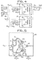
- FIG. 4 is a diagram of an embodiment of the modulation device following the invention for a 4-state phase modulation.
- the modulator is of the symmetrical double mixer type, linear for the modulating signal and has a parallel type structure. It is made with discrete elements.
- the coding device 3 supplies from the sequence of symbols 0.1 to be transmitted, two digital trains A and B containing the symbols of even rank and the symbols of odd rank, respectively, these two trains modulating in phase two carrier waves in quadrature, which are then recombined to obtain the modulated carrier.
- the modulator therefore comprises a 3dB coupler with phase shift of , 21, receiving the signal P (t) at the carrier frequency of the local oscillator 10.
- This coupler 21 shares the power it receives in equal parts P A (t) and P B (t) between two channels while 90 ° phase shift one component with respect to the other.
- These signals are respectively applied to a first input of two symmetrical mixers, 22 and 23, the second inputs of which receive the digital trains NF A and NF B respectively after filtering by the low-pass filters 41 and 42 respectively.
- These mixers each comprise two parallel paths each comprising a diode, respectively D 1 and D 2 , also connected to the terminals of an inductance coil L I whose midpoint is connected to ground.
- the diodes D 1 and D 2 are mounted head to tail.
- a second coil L 2 collects the signal resulting from the mixture of the carrier frequency signal FP (t) and the filtered digital signal, NF A (t) or NF B (t) depending on the path. These two signals are then recombined in a 0 °, 25 coupler, which does not introduce a phase shift between the two channels.
- This structure is exactly similar to that of a symmetrical double mixer with image frequency rejection, such as those which can be used in the receivers of radio-relay systems: the signal output SHF modulated is then the input of signal received, SHF modulated ; the local oscillator access SHF is then the local oscillator access FI; and the filtered digital signal input is then the intermediate frequency modulated signal output, a low-pass filter cutting the SHF frequencies being provided on each of the corresponding output arms (90 ° phase shifted).
- a mixer provides very good insulation of the carrier in a fairly wide frequency band. The measurements carried out showed, for example, that an isolation of 46 dBm was obtained in a 400 MHz band around a central frequency of 2 GHz.
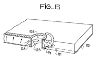
- FIG. 5 shows in plan an embodiment in integrated microelectronics of a part of the modulation device according to the invention, the integrated technology used being that of ribbon waveguides (microstrip), slotted lines, and coplanar lines.
- FIG. 6 shows a sectional view of part of the integrated circuit of Figure 5. The same elements have been designated by the same references in these two figures.
- the substrate 100 is made of a material having a high permittivity of the magnesium titanate or alumina type.
- the wave guidance is obtained in this substrate by ribbon guides produced, on one face of the substrate (front) by metallization of a ribbon, the other face (back) which constitutes the ground plane being almost entirely metallized, the electric field then being directed along the thickness of the substrate.
- Wave guidance can also be obtained by slotted lines when the impedances to be achieved are very high, since the width of the corresponding ribbon guides would be very small and difficult to achieve.
- the transition between a ribbon guide and one or two slotted lines is obtained by means of a metallized hole.
- the decoupling capacities and the diodes used are preferably flat components called "beam lead" monolithic, usable directly without the addition of other elements such as connections and housings, and easy to put in series between two coplanar lines, with ribbons or slits.
- the structure thus produced is shown in plan in FIG. 5 where the elements integrated on the front have been shown in solid lines, the elements present on the front as well as the demetallized zones corresponding to the slit lines having been represented in dotted lines.
- the 3dB coupler, 21, was produced as a ribbon guide, the incident carrier P (t) being divided into two quadrature components P A (t) and P r, (t).
- Beam lead capacities CI and C 2 are arranged on the output ribbon guides of the coupler 21. These capacities make it possible to decouple the local oscillator from the low frequency signals that are the filtered digital signals NF A (t) and NF B (t). These signals are applied to the connection terminals 101 and 102 provided on the substrate and are transmitted to the ribbon lines by means of low-pass filters with 6 microstrip elements, respectively 103 and 104, isolating the digital processing circuits from high frequencies. SHF. Metallized holes passing through the substrate, 105 and 106 allow the transition between the ribbon lines and the double slit lines.
- FIG. 6 which shows in section the substrate at the level of the hole 105, in the direction of propagation in the ribbon line, makes it possible to better understand the mode of coupling.
- This coupling by metallized hole surrounded, on the back of the substrate, by a double line with circular slot 108 makes it possible to divide the incident wave into two components, flat diodes D and D 2 being applied between the metallized central ring, 109, and the ground plane 110, across slotted and upside down lines.
- the emerging signal is transmitted in the output slit line, 111, which makes it possible to recombine the two parts of the wave resulting from the mixture P A (t) and NF A.
- the second arm of the double mixer is exactly similar to the first and the two carrier waves modulated by the filtered digital signals NF A (t) and NF B (t) are recombined in a 0 ° coupler produced using the same technique, a metallized hole 107 allowing the coupling of the waves transmitted by the slit lines of the two output arms of each symmetrical mixer to an output ribbon line forming the output of the symmetrical double mixer.
- the invention is not limited to the circuits precisely described and, for a two-state phase modulation, a modulation device which comprises a simple symmetrical mixer with two diodes, comprising a signal input and a local oscillation input, and a low-pass filter filtering the modulation signal before mixing it with the local oscillation signal in the balanced mixer is within the scope of the invention. Furthermore, the phase shift between the two components of the carrier, necessary for a 4-state modulation, can also be introduced after the modulation before recombination in the second coupler.
Landscapes
- Engineering & Computer Science (AREA)
- Computer Networks & Wireless Communication (AREA)
- Signal Processing (AREA)
- Digital Transmission Methods That Use Modulated Carrier Waves (AREA)
Applications Claiming Priority (2)
| Application Number | Priority Date | Filing Date | Title |
|---|---|---|---|
| FR8003976A FR2476947B1 (fr) | 1980-02-22 | 1980-02-22 | Dispositif de modulation numerique lineaire et emetteur hertzien comportant un tel dispositif |
| FR8003976 | 1980-02-22 |
Publications (1)
| Publication Number | Publication Date |
|---|---|
| EP0034973A1 true EP0034973A1 (fr) | 1981-09-02 |
Family
ID=9238882
Family Applications (1)
| Application Number | Title | Priority Date | Filing Date |
|---|---|---|---|
| EP81400228A Withdrawn EP0034973A1 (fr) | 1980-02-22 | 1981-02-13 | Dispositif de modulation numérique linéaire pour émetteur hertzien |
Country Status (3)
| Country | Link |
|---|---|
| EP (1) | EP0034973A1 (https=) |
| JP (1) | JPS56132047A (https=) |
| FR (1) | FR2476947B1 (https=) |
Cited By (2)
| Publication number | Priority date | Publication date | Assignee | Title |
|---|---|---|---|---|
| EP0120786A1 (fr) * | 1983-03-25 | 1984-10-03 | Alcatel Thomson Faisceaux Hertziens | Chaîne de réception hyperfréquence comportant un dispositif de démodulation directe en hyperfréquence |
| EP0139033A1 (de) * | 1983-10-21 | 1985-05-02 | ANT Nachrichtentechnik GmbH | Digitales RF-Direktmodulationsverfahren und Schaltungsanordnung zu seiner Durchführung |
Citations (2)
| Publication number | Priority date | Publication date | Assignee | Title |
|---|---|---|---|---|
| US3002159A (en) * | 1957-12-30 | 1961-09-26 | Daystrom Inc | Oscillator |
| US4216542A (en) * | 1979-03-06 | 1980-08-05 | Nasa | Method and apparatus for quadriphase-shift-key and linear phase modulation |
-
1980
- 1980-02-22 FR FR8003976A patent/FR2476947B1/fr not_active Expired
-
1981
- 1981-02-13 EP EP81400228A patent/EP0034973A1/fr not_active Withdrawn
- 1981-02-20 JP JP2415781A patent/JPS56132047A/ja active Granted
Patent Citations (2)
| Publication number | Priority date | Publication date | Assignee | Title |
|---|---|---|---|---|
| US3002159A (en) * | 1957-12-30 | 1961-09-26 | Daystrom Inc | Oscillator |
| US4216542A (en) * | 1979-03-06 | 1980-08-05 | Nasa | Method and apparatus for quadriphase-shift-key and linear phase modulation |
Non-Patent Citations (3)
| Title |
|---|
| 1979 IEEE INTERNATIONAL SOLIDSTATE CIRCUITS CONFERENCE, DIGEST OF TECHNICAL PAPERS, février 1979 New York, US AIKAWA et al.: "2Gb Double-Balanced PSK Modulator using Coplanar Waveguides", pages 172-173 * |
| MARCONI REVIEW, vol. 41, no. 210, 1978 Essex, GB BAKER et al.: "A linear 4-level PSK modulator of a new configuration", pages 129-135 * |
| MICROWAVE JOURNAL, vol. 21, no. 1, janvier 1978 DEDHAM, US ANDREN: "PSK Sidebands reduced by premodulation filtering", pages 69-73 * |
Cited By (2)
| Publication number | Priority date | Publication date | Assignee | Title |
|---|---|---|---|---|
| EP0120786A1 (fr) * | 1983-03-25 | 1984-10-03 | Alcatel Thomson Faisceaux Hertziens | Chaîne de réception hyperfréquence comportant un dispositif de démodulation directe en hyperfréquence |
| EP0139033A1 (de) * | 1983-10-21 | 1985-05-02 | ANT Nachrichtentechnik GmbH | Digitales RF-Direktmodulationsverfahren und Schaltungsanordnung zu seiner Durchführung |
Also Published As
| Publication number | Publication date |
|---|---|
| JPS6331138B2 (https=) | 1988-06-22 |
| FR2476947B1 (fr) | 1987-06-26 |
| FR2476947A1 (fr) | 1981-08-28 |
| JPS56132047A (en) | 1981-10-16 |
Similar Documents
| Publication | Publication Date | Title |
|---|---|---|
| EP0314101B1 (fr) | Système de transmission radiofréquence-optique, notamment dans le domaine des télécommunications spatiales | |
| US4612518A (en) | QPSK modulator or demodulator using subharmonic pump carrier signals | |
| WO1993006677A1 (fr) | Procede de transmission numerique et recepteur a conversion directe | |
| FR2781106A1 (fr) | Modulateur vectoriel | |
| JPH0385834A (ja) | 光周波数多重送信装置、及び、光周波数多重伝送装置 | |
| EP2074700B1 (fr) | Module d'emission et de reception radioelectrique, adapte notamment aux radiocommunications large bande | |
| FR2543379A1 (fr) | Dispositif de demodulation directe en hyperfrequence et chaine de reception hyperfrequence comportant un tel dispositif | |
| EP3188399A1 (fr) | Émetteur récepteur ibfd à module de transposition de fréquence non réciproque | |
| EP2335349B1 (fr) | Melangeur bi-mode | |
| FR2490023A1 (fr) | Melangeur hybride hyperfrequence | |
| EP0034973A1 (fr) | Dispositif de modulation numérique linéaire pour émetteur hertzien | |
| Ziemer et al. | Minimum-shift keyed modem implementations for high data rates | |
| EP2713434A1 (fr) | Dispositif routeur multiports compact | |
| US3479607A (en) | Frequency discriminator with injection-locked oscillator | |
| Linke et al. | Coherent optical detection: A thousand calls on one circuit: Dazzling applications for both long-distance and local networks are in the offing as experimental systems adapt long-successful radio techniques | |
| US4352071A (en) | Planar QPSK demodulator | |
| EP0083895B1 (fr) | Circuit hyperfréquences remplissant les fonctions de modulateur, de mélangeur et de séparateur émission-réception et dispositifs utilisant un tel circuit | |
| EP1253758B1 (fr) | Procédé de génération de modulation par division de fréquence suivi de multiplication de fréquence et équipement radiofréquence | |
| EP0011015B1 (fr) | Répéteur hertzien numérique à régénération et réseau de transmission comportant de tels répéteurs | |
| EP0097075B1 (fr) | Mélangeur d'ondes électromagnétiques hyperfréquences | |
| FR2531273A1 (fr) | Anneau hybride hyperfrequence | |
| EP0380397B1 (fr) | Modulateur équilibré pour signal électromagnétique hyperfréquence de puissance | |
| EP1014560B1 (fr) | Appareil radioélectrique comportant un synthétiseur de fréquences et procédé pour moduler en phase et/ou en fréquence un synthétiseur de fréquences. | |
| EP0599679B1 (fr) | Système de télébouclage pour émetteur-récepteur de radiotélécommunications | |
| FR2765416A1 (fr) | Etage hyperfrequence dans un emetteur ou recepteur de telecommunications |
Legal Events
| Date | Code | Title | Description |
|---|---|---|---|
| PUAI | Public reference made under article 153(3) epc to a published international application that has entered the european phase |
Free format text: ORIGINAL CODE: 0009012 |
|
| AK | Designated contracting states |
Designated state(s): AT BE CH DE GB IT LU NL SE |
|
| 17P | Request for examination filed |
Effective date: 19820115 |
|
| STAA | Information on the status of an ep patent application or granted ep patent |
Free format text: STATUS: THE APPLICATION IS DEEMED TO BE WITHDRAWN |
|
| 18D | Application deemed to be withdrawn |
Effective date: 19831212 |
|
| RIN1 | Information on inventor provided before grant (corrected) |
Inventor name: CURTINOT, JEAN-CLAUDE |