EP0033882B1 - Process for the manufacture of an optically active surface element - Google Patents
Process for the manufacture of an optically active surface element Download PDFInfo
- Publication number
- EP0033882B1 EP0033882B1 EP81100533A EP81100533A EP0033882B1 EP 0033882 B1 EP0033882 B1 EP 0033882B1 EP 81100533 A EP81100533 A EP 81100533A EP 81100533 A EP81100533 A EP 81100533A EP 0033882 B1 EP0033882 B1 EP 0033882B1
- Authority
- EP
- European Patent Office
- Prior art keywords
- grid
- etching
- optically active
- light
- incident
- Prior art date
- Legal status (The legal status is an assumption and is not a legal conclusion. Google has not performed a legal analysis and makes no representation as to the accuracy of the status listed.)
- Expired
Links
- 238000004519 manufacturing process Methods 0.000 title claims abstract description 12
- 238000000034 method Methods 0.000 title claims abstract description 11
- 238000005530 etching Methods 0.000 claims abstract description 17
- 238000004090 dissolution Methods 0.000 claims abstract 4
- 230000001747 exhibiting effect Effects 0.000 claims abstract 3
- 239000000463 material Substances 0.000 claims description 9
- 239000002184 metal Substances 0.000 claims description 8
- 230000001934 delay Effects 0.000 claims description 3
- 238000000465 moulding Methods 0.000 claims description 3
- 238000007639 printing Methods 0.000 claims description 2
- 238000010137 moulding (plastic) Methods 0.000 claims 1
- 239000004744 fabric Substances 0.000 description 12
- 230000001788 irregular Effects 0.000 description 4
- 238000003384 imaging method Methods 0.000 description 2
- 230000003287 optical effect Effects 0.000 description 2
- 239000000654 additive Substances 0.000 description 1
- 230000000996 additive effect Effects 0.000 description 1
- 238000005516 engineering process Methods 0.000 description 1
- 230000004907 flux Effects 0.000 description 1
- 239000011888 foil Substances 0.000 description 1
- 239000011159 matrix material Substances 0.000 description 1
- 230000004304 visual acuity Effects 0.000 description 1
Images
Classifications
-
- G—PHYSICS
- G03—PHOTOGRAPHY; CINEMATOGRAPHY; ANALOGOUS TECHNIQUES USING WAVES OTHER THAN OPTICAL WAVES; ELECTROGRAPHY; HOLOGRAPHY
- G03F—PHOTOMECHANICAL PRODUCTION OF TEXTURED OR PATTERNED SURFACES, e.g. FOR PRINTING, FOR PROCESSING OF SEMICONDUCTOR DEVICES; MATERIALS THEREFOR; ORIGINALS THEREFOR; APPARATUS SPECIALLY ADAPTED THEREFOR
- G03F7/00—Photomechanical, e.g. photolithographic, production of textured or patterned surfaces, e.g. printing surfaces; Materials therefor, e.g. comprising photoresists; Apparatus specially adapted therefor
- G03F7/0005—Production of optical devices or components in so far as characterised by the lithographic processes or materials used therefor
- G03F7/001—Phase modulating patterns, e.g. refractive index patterns
-
- G—PHYSICS
- G03—PHOTOGRAPHY; CINEMATOGRAPHY; ANALOGOUS TECHNIQUES USING WAVES OTHER THAN OPTICAL WAVES; ELECTROGRAPHY; HOLOGRAPHY
- G03C—PHOTOSENSITIVE MATERIALS FOR PHOTOGRAPHIC PURPOSES; PHOTOGRAPHIC PROCESSES, e.g. CINE, X-RAY, COLOUR, STEREO-PHOTOGRAPHIC PROCESSES; AUXILIARY PROCESSES IN PHOTOGRAPHY
- G03C1/00—Photosensitive materials
- G03C1/76—Photosensitive materials characterised by the base or auxiliary layers
-
- G—PHYSICS
- G03—PHOTOGRAPHY; CINEMATOGRAPHY; ANALOGOUS TECHNIQUES USING WAVES OTHER THAN OPTICAL WAVES; ELECTROGRAPHY; HOLOGRAPHY
- G03F—PHOTOMECHANICAL PRODUCTION OF TEXTURED OR PATTERNED SURFACES, e.g. FOR PRINTING, FOR PROCESSING OF SEMICONDUCTOR DEVICES; MATERIALS THEREFOR; ORIGINALS THEREFOR; APPARATUS SPECIALLY ADAPTED THEREFOR
- G03F7/00—Photomechanical, e.g. photolithographic, production of textured or patterned surfaces, e.g. printing surfaces; Materials therefor, e.g. comprising photoresists; Apparatus specially adapted therefor
- G03F7/0005—Production of optical devices or components in so far as characterised by the lithographic processes or materials used therefor
- G03F7/0007—Filters, e.g. additive colour filters; Components for display devices
Definitions
- the invention relates to a method for producing an optically active fabric which bundles light falling on a diffusely reflecting surface in a direction perpendicular to this surface.
- optically active sheets are used in the projection of images with an optical projector (US-A-3 269 839, US-A-4175844 and others).
- the disadvantage of the previously known optically active fabrics of this type is that their resolving power is extremely poor, so that their use has been limited to a few cases in which only very coarse patterns were to be reproduced.
- color line grids There are various methods of making color line grids, e.g. for additive color photography (DE-A-1 1 003582), but also for spectrography (DE-A-1 623 803), which are produced by solution or etching. There are essentially three methods that can be used here: A method in which a dot is placed on a transparent support with a photosensitive layer, the parts of which are struck by light and have a different solubility or etchability than the parts which are not struck by light.
- a dot or line raster is optically imaged, a method in which a dot or line raster is printed on a transparent plate or film consisting of soluble or etchable material from a material preventing or delaying the solution or etching, and a method in which a Metal plate with a photosensitive layer, the parts of which have been hit by light have a different etchability than the parts which are not hit by light, a dot or line pattern is optically imaged, after which the etching is carried out, after which a plastic imaging or molding of the surface of the metal plate onto the surface a transparent film or pla tte is done.
- This problem can be solved in three ways: by a method for producing an optically active fabric, in which a transparent support with a photosensitive layer, the parts of which are struck by light and have a different solubility or etchability than the part which is not struck by light Dot or line raster is optically imaged, characterized in that a raster is imaged in which one or more raster elements are provided per square millimeter, and that the solution or etching is carried out until raised cylinder parts or spherical parts in the photosensitive layer or become visible in the carrier.
- a dot or line grid is printed on a transparent plate or film consisting of soluble or etchable material, which material prevents or delays the solution or etching, which is characterized in that a Grid is printed on, in which one or more grid elements are provided per square millimeter, and that the solution or etching is carried out until raised cylinder parts or spherical parts in the material preventing the solution or etching, in the plate or in the film is visible will.
- FIG. 5 shows a view from above of a flat structure with a grid of cylinder parts in a regular arrangement, in FIG. 6 in an irregular arrangement.
Landscapes
- Physics & Mathematics (AREA)
- General Physics & Mathematics (AREA)
- Chemical & Material Sciences (AREA)
- Engineering & Computer Science (AREA)
- Materials Engineering (AREA)
- Weting (AREA)
- Electrodes Of Semiconductors (AREA)
- Moulds For Moulding Plastics Or The Like (AREA)
- Optical Integrated Circuits (AREA)
- Optical Elements Other Than Lenses (AREA)
- Surface Treatment Of Glass (AREA)
Abstract
Description
Die Erfindung betrifft ein Verfahren zur Herstellung eines optisch aktiven Flächengebildes, welches auf eine diffus reflektierende Fläche fallendes Licht in einer Richtung senkrecht zu dieser Fläche bündelt.The invention relates to a method for producing an optically active fabric which bundles light falling on a diffusely reflecting surface in a direction perpendicular to this surface.
Derartige optisch aktive Flächengebilde werden bei der Projektion von Bildern mit einem optischen Projektor angewandt (US-A-3 269 839, US-A-4175844 u.a.). Nachteil der bisher bekannten optisch aktiven Flächengebilde dieser Art ist es, dass ihr Auflösevermögen äusserst schlecht ist, so dass ihre Anwendung auf wenige Fälle beschränkt blieb, bei denen nur sehr grobe Muster abzubilden waren.Such optically active sheets are used in the projection of images with an optical projector (US-A-3 269 839, US-A-4175844 and others). The disadvantage of the previously known optically active fabrics of this type is that their resolving power is extremely poor, so that their use has been limited to a few cases in which only very coarse patterns were to be reproduced.
Es sind verschiedene Verfahren zur Herstellung von Farblinienrastern, z.B. für die additive Farbenphotographie (DE-A-1 1 003582), aber auch für die Spektrographie (DE-A-1 623 803) bekannt geworden, die durch Lösung oder Ätzung hergestellt werden. Hier sind es im wesentlichen drei Verfahren, die zur Anwendung kommen können: Ein Verfahren, bei dem auf einen durchsichtigen Träger mit einer photoempfindlichen Schicht, deren von Licht getroffene Teile eine andere Löslichkeit oder Ätzbarkeit als die nicht von Licht getroffenen Teile aufweisen, ein Punkt- oder Linienraster optisch abgebildet wird, ein Verfahren, bei dem auf eine durchsichtige, aus löslichem oder ätzbarem Material bestehende Platte oder Folie ein Punkt- oder Linienraster aus einem die Lösung oder Ätzung verhindernden oder verzögernden Material aufgedruckt wird, und ein Verfahren, bei dem auf eine Metallplatte mit photoempfindlicher Schicht, deren von Licht getroffene Teile eine andere Ätzbarkeit als die nicht vom Licht getroffenen Teile aufweisen, ein Punkt- oder Linienraster optisch abgebildet wird, wonach die Ätzung durchgeführt wird, wonach eine plastische Abbildung oder Abformung der Oberfläche der Metallplatte auf die Oberfläche einer durchsichtigen Folie oder Platte erfolgt.There are various methods of making color line grids, e.g. for additive color photography (DE-A-1 1 003582), but also for spectrography (DE-A-1 623 803), which are produced by solution or etching. There are essentially three methods that can be used here: A method in which a dot is placed on a transparent support with a photosensitive layer, the parts of which are struck by light and have a different solubility or etchability than the parts which are not struck by light. or line raster is optically imaged, a method in which a dot or line raster is printed on a transparent plate or film consisting of soluble or etchable material from a material preventing or delaying the solution or etching, and a method in which a Metal plate with a photosensitive layer, the parts of which have been hit by light have a different etchability than the parts which are not hit by light, a dot or line pattern is optically imaged, after which the etching is carried out, after which a plastic imaging or molding of the surface of the metal plate onto the surface a transparent film or pla tte is done.
Es ist die Aufgabe der vorliegenden Erfindung, mit einfachen Mitteln eine Möglichkeit zu schaffen, ein optisch aktives Flächengebilde herzustellen, welches mit grosser Auflösung das auf eine diffus reflektierende Fläche fallende Licht in einer Richtung senkrecht zu dieser Fläche bündelt.It is the object of the present invention to provide, with simple means, a possibility of producing an optically active flat structure which bundles the light falling on a diffusely reflecting surface in a direction perpendicular to this surface with high resolution.
Diese Aufgabe lässt sich auf dreierlei Weise lösen: Durch ein Verfahren zur Herstellung eines optisch aktiven Flächengebildes, bei dem auf einen durchsichtigen Träger mit einer photoempfindlichen Schicht, deren von Licht getroffenen Teile eine andere Löslichkeit oder Ätzbarkeit als die nicht von Licht getroffenen Teil aufweisen, ein Punkt- oder Linienraster optisch abgebildet wird, dass dadurch gekennzeichnet ist, dass ein Raster abgebildet wird, bei dem ein oder mehrere Rasterelemente pro Quadratmillimeter vorgesehen sind, und dass die Lösung oder Ätzung so lange durchgeführt wird, bis erhabene Zylinderteile oder Kugelteile in der photoempfindlichen Schicht oder im Träger sichtbar werden.This problem can be solved in three ways: by a method for producing an optically active fabric, in which a transparent support with a photosensitive layer, the parts of which are struck by light and have a different solubility or etchability than the part which is not struck by light Dot or line raster is optically imaged, characterized in that a raster is imaged in which one or more raster elements are provided per square millimeter, and that the solution or etching is carried out until raised cylinder parts or spherical parts in the photosensitive layer or become visible in the carrier.
Durch ein Verfahren zur Herstellung eines optisch aktiven Flächengebildes, bei dem auf eine durchsichtige, aus löslichem oder ätzbarem Material bestehende Platte oder Folie ein Punkt- oder Linienraster aus einem die Lösung oder Ätzung verhindernden oder verzögernden Material aufgedruckt wird, das dadurch gekennzeichnet ist, dass ein Raster aufgedruckt wird, bei dem ein oder mehrere Rasterelemente pro Quadratmillimeter vorgesehen sind, und dass die Lösung oder Ätzung so lange durchgeführt wird, bis erhabene Zylinderteile oder Kugelteile in dem die Lösung oder Ätzung verhindernden oder verzögernden Material, in der Platte oder in der Folie sichtbar werden.By means of a method for producing an optically active sheet-like structure, in which a dot or line grid is printed on a transparent plate or film consisting of soluble or etchable material, which material prevents or delays the solution or etching, which is characterized in that a Grid is printed on, in which one or more grid elements are provided per square millimeter, and that the solution or etching is carried out until raised cylinder parts or spherical parts in the material preventing the solution or etching, in the plate or in the film is visible will.
Durch ein Verfahren zur Herstellung eines optisch aktiven Flächengebildes, bei dem auf eine Metallplatte mit photoempfindlicher Schicht, deren von Licht getroffene Teile eine andere Ätzbarkeit als die nicht vom Licht getroffenen Teile aufweisen, ein Punkt- oder Linienraster optisch abgebildet wird, wonach die Ätzung durchgeführt wird, wonach eine plastische Abbildung oder Abformung der Oberfläche der Metallplatte auf die Oberfläche einer durchsichtigen Folie oder Platte erfolgt, das dadurch gekennzeichnet ist, dass ein Raster abgebildet wird, bei dem ein oder mehrere Rasterelemente pro Quadratmillimeter vorgesehen sind, und dass die Ätzung so lange durchgeführt wird, bis die Oberfläche der Metallplatte für die Abformung erhabener Zylinderteile oder Kugelteile geeignet ist.By means of a method for producing an optically active sheet-like structure, in which a dot or line grid is optically imaged on a metal plate with a photosensitive layer, the parts of which have been hit by light have a different etchability than the parts which have not been hit by light, after which the etching is carried out , whereupon a plastic imaging or molding of the surface of the metal plate onto the surface of a transparent film or plate takes place, which is characterized in that a raster is imaged in which one or more raster elements are provided per square millimeter, and that the etching is carried out for so long until the surface of the metal plate is suitable for taking raised cylindrical or spherical parts.
Wird ein derartiges Flächengebilde auf eine diffus reflektierende Vorlage gelegt, so wird auch seitlich auf die Vorlage fallendes Licht senkrecht zur Vorlage gebündelt reflektiert. Dadurch wird ein hoher Lichtstrom in Richtung senkrecht zur Oberfläche des Flächengebildes erzeugt. Die einzelnen Kugel- und/oder Zylinderteile weisen dabei Grössen auf, die an mikroskopische Grössen grenzen. Hierdurch wird eine hohe Auflösung erzielt.If such a flat structure is placed on a diffusely reflecting template, then light falling on the template laterally is also reflected in a bundle perpendicular to the template. This creates a high luminous flux in the direction perpendicular to the surface of the fabric. The individual spherical and / or cylindrical parts have sizes that border on microscopic sizes. As a result, a high resolution is achieved.
Das Wesen der Erfindung ist nachstehend anhand von in der Zeichnung schematisch dargestellten Ausführungsbeispielen näher erläutert. Es zeigen:
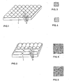
- Fig. 1 eine perspektivische Ansicht eines kleinen Teiles aus einem optisch aktiven Flächengebilde mit einem Punktraster.
- Fig. 2 ein kleines Teil aus einem optisch aktiven Flächengebilde mit einem Linienraster.
- Fig. eine Ansicht eines kleines Teiles eines optisch aktiven Flächengebildes mit Punktraster in regelmässiger Anordnung.
- Fig. 4 einen kleinen Ausschnitt aus der Ansicht eines optisch aktiven Flächengebildes mit Punktraster in unregelmässiger Anordnung.
- Fig. einen kleinen Ausschnitt aus einem optisch aktiven Flächengebilde mit Linienraster in regelmässiger Anordnung.
- Fig. einen kleinen Ausschnitt aus einer Ansicht eines optisch aktiven Flächengebildes mit Linienraster in unregelmässiger Anordnung.
- Fig. 1 is a perspective view of a small part of an optically active fabric with a dot pattern.
- Fig. 2 shows a small part from an optically active fabric with a line grid.
- Fig. A view of a small part of an optically active fabric with a dot pattern in a regular arrangement.
- Fig. 4 shows a small section from the view of an optically active fabric with a dot pattern in an irregular arrangement.
- Fig. A small section of an optically active fabric with a line grid in a regular arrangement.
- Fig. A small section of a view of an optically active fabric with a line grid in an irregular arrangement.
Alle Zeichnungsfiguren sind in starker Vergrösserung dargestellt. Denn pro Quadratmillimeter sind mehrere Rasterelemente vorgesehen.
- Im Ausführungsbeispiel der Fig. 1 ist die Oberfläche der Folie 1 mit
Rasterelementen 2 versehen, die die Gestalt eines Teiles einer Kugel aufweisen und die regelmässig angeordnet sind. - Im Ausführungsbeispiel der Fig. 2 weist die Oberfläche der Folie 1 zylinderteilförmige Erhebungen in regelmässiger Rasteranordnung auf. Die perspektivischen Ansichten der Fig. 1 und 2 sind dabei sehr stark vergrössert.
- Im Ausführungsbeispiel der Fig. 3 ist eine Ansicht von oben auf einen Punktraster von Kugelteilelementen auf der Oberfläche dargestellt. In Fig. 4 ist diese Anordnung unregelmässig.
- In the exemplary embodiment in FIG. 1, the surface of the film 1 is provided with
raster elements 2 which have the shape of part of a sphere and which are arranged regularly. - In the exemplary embodiment of FIG. 2, the surface of the film 1 has elevations in the form of cylindrical parts in a regular grid arrangement. The perspective views of FIGS. 1 and 2 are greatly enlarged.
- In the exemplary embodiment in FIG. 3, a view from above of a dot matrix of spherical part elements is shown on the surface. In Fig. 4 this arrangement is irregular.
In Fig. 5 ist eine Ansicht von oben auf ein Flächengebilde mit einem Raster von Zylinderteilen in regelmässiger Anordnung gezeigt, in Fig. 6 in unregelmässiger Anordnung.5 shows a view from above of a flat structure with a grid of cylinder parts in a regular arrangement, in FIG. 6 in an irregular arrangement.
Vorteile dieses optisch aktiven Flächengebildes sind:
- Starke Bündelung des von einer unter dem Flächengebilde liegenden Vorlage diffus reflektierenden Lichtes in Richtung senkrecht zur Ebene der Fläche.
- Strong bundling of the light diffusely reflecting from a template lying under the fabric in the direction perpendicular to the plane of the surface.
Leichte Herstellbarkeit nach aus der Drucktechnik bekannten Ätz- und Lösungsvorgängen.Easy to manufacture using etching and solution processes known from printing technology.
Ausführbarkeit an den verschiedensten Materialien entweder durch direkte Lösung oder durch Abformung von einer geätzten Vorlage.Feasibility on a wide variety of materials either by direct solution or by taking an impression from an etched template.
Herstellungsmöglichkeit in ebenen Platten.Possibility of production in flat plates.
Herstellungmöglichkeit in biegsamen Folien.Possibility of production in flexible foils.
Anwendbarkeit in verschiedenen optischen Geräten.Applicability in various optical devices.
Anwendbarkeit durch Aufkleben auf die diffus reflektierende Vorlage.Applicability by sticking on the diffusely reflective template.
Claims (3)
Priority Applications (1)
| Application Number | Priority Date | Filing Date | Title |
|---|---|---|---|
| AT81100533T ATE15413T1 (en) | 1980-01-25 | 1981-01-25 | PROCESS FOR MANUFACTURING AN OPTICALLY ACTIVE PLAN. |
Applications Claiming Priority (2)
| Application Number | Priority Date | Filing Date | Title |
|---|---|---|---|
| CH58880 | 1980-01-25 | ||
| CH588/80 | 1980-01-25 |
Publications (3)
| Publication Number | Publication Date |
|---|---|
| EP0033882A2 EP0033882A2 (en) | 1981-08-19 |
| EP0033882A3 EP0033882A3 (en) | 1982-06-30 |
| EP0033882B1 true EP0033882B1 (en) | 1985-09-04 |
Family
ID=4190473
Family Applications (1)
| Application Number | Title | Priority Date | Filing Date |
|---|---|---|---|
| EP81100533A Expired EP0033882B1 (en) | 1980-01-25 | 1981-01-25 | Process for the manufacture of an optically active surface element |
Country Status (3)
| Country | Link |
|---|---|
| EP (1) | EP0033882B1 (en) |
| AT (1) | ATE15413T1 (en) |
| DE (1) | DE3172095D1 (en) |
Families Citing this family (1)
| Publication number | Priority date | Publication date | Assignee | Title |
|---|---|---|---|---|
| CA2071598C (en) * | 1991-06-21 | 1999-01-19 | Akira Eda | Optical device and method of manufacturing the same |
Family Cites Families (14)
| Publication number | Priority date | Publication date | Assignee | Title |
|---|---|---|---|---|
| GB191409929A (en) * | 1914-04-22 | 1915-04-22 | Julius Rheinberg | Improved Methods in the Production and use of Screens for Colour Photography and General Photographic Purposes. |
| DE326711C (en) * | 1915-03-10 | 1920-09-30 | Julius Rheinberg | Process for the production of single and multicolor screens for color photography and general photographic purposes |
| DE1003582B (en) * | 1955-01-18 | 1957-02-28 | Emimeta Fabrikations Anstalt | Color line grid for additive color photography, in which the grid area is divided into fields, and process for its production |
| USB322986I5 (en) * | 1963-01-04 | |||
| GB1120467A (en) * | 1964-08-19 | 1968-07-17 | Mason & Sons Ltd E N | Improvements in inks and other film-forming media |
| DE1623803B2 (en) * | 1967-02-11 | 1971-11-11 | Rudolph, Dietbert, Dipl.-Phys., 3401 Menger shausen; Schmahl, Günter, Dipl.-Phys. Dr., 3400 Göttingen | METHOD OF MANUFACTURING REFLECTION AND TRANSMISSION GRIDS |
| DE1798372A1 (en) * | 1967-03-28 | 1972-08-10 | Rudolph Dietbert Dipl Phys | Process for the production of reflection and transmission gratings |
| US3584369A (en) * | 1967-10-11 | 1971-06-15 | Roger Lannes De Montebello | Process of making reinforced lenticular sheet |
| GB1280625A (en) * | 1970-02-26 | 1972-07-05 | Nat Res Dev | Method of forming fringe pattern images |
| GB1462618A (en) * | 1973-05-10 | 1977-01-26 | Secretary Industry Brit | Reducing the reflectance of surfaces to radiation |
| FR2256423A1 (en) * | 1973-12-28 | 1975-07-25 | Pointu Pierre | Light beam selector for projection screens - has mask transmitting light to series of parallel lenses |
| DE2409702A1 (en) * | 1974-02-28 | 1975-09-04 | Agfa Gevaert Ag | Photoelectric element for measuring light intensity - has raster of lenslets to focus incident light on individual sensitive spots |
| IL48318A0 (en) * | 1975-10-19 | 1975-12-31 | Yeda Res & Dev | Thin optical imaging device |
| US4175844A (en) * | 1975-10-19 | 1979-11-27 | Yeda Research & Development Co. Ltd. | Optical imaging system |
-
1981
- 1981-01-25 DE DE8181100533T patent/DE3172095D1/en not_active Expired
- 1981-01-25 AT AT81100533T patent/ATE15413T1/en not_active IP Right Cessation
- 1981-01-25 EP EP81100533A patent/EP0033882B1/en not_active Expired
Also Published As
| Publication number | Publication date |
|---|---|
| EP0033882A3 (en) | 1982-06-30 |
| DE3172095D1 (en) | 1985-10-10 |
| ATE15413T1 (en) | 1985-09-15 |
| EP0033882A2 (en) | 1981-08-19 |
Similar Documents
| Publication | Publication Date | Title |
|---|---|---|
| DE69404042T2 (en) | AN ARRANGEMENT OF A COMPOSED IMAGE | |
| AT401587B (en) | DISPLAY DEVICE WITH A GRID BODY | |
| DE3004749A1 (en) | DEVICE AND METHOD FOR THE DIGITALLY CONTROLLED PRODUCTION OF PRINTING FORMS USING A LASER | |
| DE3602563C1 (en) | Security paper with optically active structures generating a moiré effect | |
| DE2627247C2 (en) | Scanner for the recording of halftone screen dots, which are made up of linearly exposed areas | |
| EP0873006A3 (en) | Photoplotting method and apparatus for recording a computer-stored raster image on an even, light-sensitive recording medium | |
| DE2214728C3 (en) | Process for the direct photomechanical production of screen printing forms | |
| EP0033882B1 (en) | Process for the manufacture of an optically active surface element | |
| DE2805874B2 (en) | Method for producing a gravure form | |
| DE3130182A1 (en) | Guilloche grid | |
| DE2141839B2 (en) | ||
| DE2002605B2 (en) | Process for the production of a shadow mask for a color television tube | |
| EP0000570A1 (en) | Original of an optical information carrier and process for realising this original | |
| DE961680C (en) | Process for the production of autotypical intaglio printing forms for the autotypical intaglio printing process and the grids for the execution of the same | |
| DE92835C (en) | ||
| DE2447268C3 (en) | Imaging system for electrophotographic half-phone reproduction | |
| DE109098C (en) | ||
| DE147523C (en) | ||
| DE2656173C3 (en) | ||
| DE226614C (en) | PROCESS FOR THE PRODUCTION OF CORNED OR DISCONNECTED PHOTOGRAPHICAL IMAGES | |
| DE3228387A1 (en) | Method of screening halftone image motifs | |
| AT152356B (en) | Screen, especially for gravure printing technology and process for its production. | |
| DE272016C (en) | ||
| DE2362843A1 (en) | METHOD OF DISPLAYING AN IMAGE ON A CONFIRMATION CARD OR THE SAME AND IMAGE CARRIER IN THE FORM OF A CONFIRMATION CARD OR THE SAME | |
| DE767469C (en) | Process for the production of copyable positives for flat and offset printing forms |
Legal Events
| Date | Code | Title | Description |
|---|---|---|---|
| PUAI | Public reference made under article 153(3) epc to a published international application that has entered the european phase |
Free format text: ORIGINAL CODE: 0009012 |
|
| AK | Designated contracting states |
Designated state(s): AT BE DE FR GB IT NL SE |
|
| PUAL | Search report despatched |
Free format text: ORIGINAL CODE: 0009013 |
|
| AK | Designated contracting states |
Designated state(s): AT BE DE FR GB IT NL SE |
|
| 17P | Request for examination filed |
Effective date: 19821216 |
|
| ITF | It: translation for a ep patent filed | ||
| GRAA | (expected) grant |
Free format text: ORIGINAL CODE: 0009210 |
|
| AK | Designated contracting states |
Designated state(s): AT BE DE FR GB IT NL SE |
|
| REF | Corresponds to: |
Ref document number: 15413 Country of ref document: AT Date of ref document: 19850915 Kind code of ref document: T |
|
| REF | Corresponds to: |
Ref document number: 3172095 Country of ref document: DE Date of ref document: 19851010 |
|
| ET | Fr: translation filed | ||
| PLBE | No opposition filed within time limit |
Free format text: ORIGINAL CODE: 0009261 |
|
| STAA | Information on the status of an ep patent application or granted ep patent |
Free format text: STATUS: NO OPPOSITION FILED WITHIN TIME LIMIT |
|
| 26N | No opposition filed | ||
| PGFP | Annual fee paid to national office [announced via postgrant information from national office to epo] |
Ref country code: AT Payment date: 19870129 Year of fee payment: 7 |
|
| PGFP | Annual fee paid to national office [announced via postgrant information from national office to epo] |
Ref country code: NL Payment date: 19870131 Year of fee payment: 7 |
|
| PG25 | Lapsed in a contracting state [announced via postgrant information from national office to epo] |
Ref country code: AT Effective date: 19880125 |
|
| PG25 | Lapsed in a contracting state [announced via postgrant information from national office to epo] |
Ref country code: SE Effective date: 19880126 |
|
| BERE | Be: lapsed |
Owner name: DEMOLUX G.M.B.H. & CO. K.G. Effective date: 19880131 |
|
| PG25 | Lapsed in a contracting state [announced via postgrant information from national office to epo] |
Ref country code: NL Effective date: 19880801 |
|
| NLV4 | Nl: lapsed or anulled due to non-payment of the annual fee | ||
| GBPC | Gb: european patent ceased through non-payment of renewal fee | ||
| PG25 | Lapsed in a contracting state [announced via postgrant information from national office to epo] |
Ref country code: FR Free format text: LAPSE BECAUSE OF NON-PAYMENT OF DUE FEES Effective date: 19880930 |
|
| PG25 | Lapsed in a contracting state [announced via postgrant information from national office to epo] |
Ref country code: DE Effective date: 19881001 |
|
| PG25 | Lapsed in a contracting state [announced via postgrant information from national office to epo] |
Ref country code: GB Free format text: LAPSE BECAUSE OF NON-PAYMENT OF DUE FEES Effective date: 19881118 |
|
| REG | Reference to a national code |
Ref country code: FR Ref legal event code: ST |
|
| PG25 | Lapsed in a contracting state [announced via postgrant information from national office to epo] |
Ref country code: BE Effective date: 19890131 |
|
| EUG | Se: european patent has lapsed |
Ref document number: 81100533.9 Effective date: 19880913 |