EP0033067B1 - Printer system - Google Patents
Printer system Download PDFInfo
- Publication number
- EP0033067B1 EP0033067B1 EP81100079A EP81100079A EP0033067B1 EP 0033067 B1 EP0033067 B1 EP 0033067B1 EP 81100079 A EP81100079 A EP 81100079A EP 81100079 A EP81100079 A EP 81100079A EP 0033067 B1 EP0033067 B1 EP 0033067B1
- Authority
- EP
- European Patent Office
- Prior art keywords
- parity
- subscan
- accordance
- printer system
- fire
- Prior art date
- Legal status (The legal status is an assumption and is not a legal conclusion. Google has not performed a legal analysis and makes no representation as to the accuracy of the status listed.)
- Expired
Links
Images


Classifications
-
- G—PHYSICS
- G06—COMPUTING OR CALCULATING; COUNTING
- G06F—ELECTRIC DIGITAL DATA PROCESSING
- G06F11/00—Error detection; Error correction; Monitoring
- G06F11/07—Responding to the occurrence of a fault, e.g. fault tolerance
- G06F11/08—Error detection or correction by redundancy in data representation, e.g. by using checking codes
- G06F11/10—Adding special bits or symbols to the coded information, e.g. parity check, casting out 9's or 11's
-
- B—PERFORMING OPERATIONS; TRANSPORTING
- B41—PRINTING; LINING MACHINES; TYPEWRITERS; STAMPS
- B41J—TYPEWRITERS; SELECTIVE PRINTING MECHANISMS, i.e. MECHANISMS PRINTING OTHERWISE THAN FROM A FORME; CORRECTION OF TYPOGRAPHICAL ERRORS
- B41J9/00—Hammer-impression mechanisms
- B41J9/44—Control for hammer-impression mechanisms
- B41J9/52—Control for hammer-impression mechanisms for checking the operation of print hammers
-
- G—PHYSICS
- G06—COMPUTING OR CALCULATING; COUNTING
- G06K—GRAPHICAL DATA READING; PRESENTATION OF DATA; RECORD CARRIERS; HANDLING RECORD CARRIERS
- G06K15/00—Arrangements for producing a permanent visual presentation of the output data, e.g. computer output printers
- G06K15/02—Arrangements for producing a permanent visual presentation of the output data, e.g. computer output printers using printers
- G06K15/08—Arrangements for producing a permanent visual presentation of the output data, e.g. computer output printers using printers by flight printing with type font moving in the direction of the printed line, e.g. chain printers
Definitions
- This invention relates to a printer system in accordance with the preamble of claim 1 and particularly to controls for parity checking print hammers of high speed belt printers.
- print hammer checking arrangements commonly use feedback or echo signals from hammer operating circuits. These are compared one-on-one with activating or selection signals of the hammer operating signals. Since hammer selection and hammer occur in advance of the generation of the echo signals a certain amount of overlap is required to print at higher operating speeds. To permit overlap, the hammer selection and echo signals are first stored in separate memories and their contents compared for checking at a later time in the printing cycle. In some cases the generation of echo signals of a later subcycle overlaps the checking of the echo signals of a preceding subcycle.
- the following U.S. patents are representative of the prior art: 3,066,601, issued December 4, 1962 to Harold E. Eden; 3,246,292, issued April 12, 1966 to W. D.
- U.S. patent 3,474,956, issued October 28, 1969 to P. A. Cain describes a punch machine or drum printer which uses parity checking.
- a punch selection parity signal generated concurrently with the punch electromagnet selection is stored in a time delay circuit for later comparison with a timed punch operation parity signal occurring later in the operating cycle.
- the use of memory in timing of punch cycle operations allows punch selection to overlap the parity checking, each punching operation being checked separately.
- U.S. Patent 4,008,389 issued February 15, 1977 to J. Brunin, et al, describes a print hammer error checking arrangement for a belt printer in which characters and hammers are aligned in subcycles or subscans. Error detectors are combined with the hammer amplifier circuits which operate the print hammers. In the event the selected amplifier circuit fails to operate, an error signal is generated which is gated through an error detection matrix to an error register which records the number of the column and the number of the subcycle in which the error occurred. Flip-flops are set when an error is gated through the matrix and are then checked at the end of printing a line.
- the invention is preferably practiced in a control system using a microprocessor for controlling all the described checking selection and activating functions which include generating the expected parity, computing and updating the composite parity, and comparing the composite parity with the actual parity.
- Microprocessors operate at relatively high speeds and can be easily programmed to perform the various checking and control operations for operating belt printers at sustained high operating speeds.
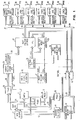
- FIG. 1 shows a printer system which controls the printing operations of a belt type printer mechanism.
- the printer mechanism includes a row of print hammers and revolving type belt or similar linear type carrier by which characters are movable continuously past the print hammers. Because of differences in the pitch of the print hammers and the characters, printing occurs on the basis of scans and subscans in which various groups of characters are aligned/optioned to various groups of hammers which are selectively operated to record characters on a print medium.
- the subscan alignment sequences are repetitive throughout the printing cycle which could include one or more lines of data printed in succession at high printing rates.
- lines of data stored in a random access memory RAM 10 are rearranged therein into a printing algorithm by a microprocessing unit MPU 11 in accordance with suitable microprogramming contained in a read-only storage ROS 12.
- the printing algorithm includes various tables including a subscan table SST and a print position fire table PPFT the latter of which contains the print position fire data organized in subscan order to be used by MPU 11 for controlling the operation of the print hammers optioned with characters in the subscan sequences.
- expected parity is also stored in the PPFT with the subscan fire data. More particularly, MPU 11 calculates the expected parity during the building of the print position fibre table. Specifically, each print position added to the print position fire table in a subscan results in MPU 11 calculating and recalculating the expected parity for that subscan and storing it in the storage location following the last position in the print position fire table.
- Address connections for MPU 11 to ROS 12 and RAM 10 comprise Address Bus 13, Address Selector 14 and Address Bus 15.
- Address Bus 15 also connects Address Selector 14 to a multiplexor MPXR 16.
- Address Bus 13 is further connected to MPU decode 17 which generates various gating CHIP SEL signals to Tri-State devices TSD 18, 19 and 20 as well as to MPXR 16.
- Data used by MPU 11 for building the printing algorithm tables and for controlling print hammer operation as well as for parity calculation and checking flows from ROS 12 on Data Bus 21 through TSD 19 and from RAM 10 and MPXR 16 on Data Bus 22 through TSD 18 and bus 23 to MPU 11 and on Data Bus 24 to .TSD 20 from MPU 11.
- MPU 11 addresses the subscan locations in the subscan table in RAM 10 which contain an indirect address pointing to an address in the PPFT where a print position count followed by one or more bytes of fire data for the print positions corresponding to the print hammers to be fired as well as the expected parity for that corresponding subscan.
- the fire data which in the preferred embodiment is an 8-bit byte per print position is sent by MPU 11 on bus 24 through TSD 20 to the input of a hammer position decode HPD 25.
- HPD 25 converts the 8-bit print position fire data into a 16X and 9Y code which is sent by a gating pulse on line 39 from MPU 11 onto bus 26 to the print position latches PPL27.
- Each hammer driver card HDC 1-6 contains twenty-two hammer operating circuits designated ODD or EVEN for energizing, when selected, a corresponding number of odd or even numbered hammer operating coils 30.
- HDC-1 contains twenty-two driver circuits for the coils 30 connected to hammers at the odd-numbered print positions 1-43.
- HDC-2 contains a like number of driver circuits for coils 30 of the even-numbered print positions 2-44, and so on, as shown in FIG. 1.
- the HDC's contain parity circuits associated with the hammer operating circuits and are designed to supply the six ODD/EVEN PARITY 1-6 signals on the feedback connections shown in FIG. 1 to MPXR 16 via bus 34.
- Each card contains a parity return signal indicating whether the real time actuated driver circuits contain an EVEN or ODD count.
- the six ODD/EVEN PARITY 1-6 signals are constantly present on the bus 34 and constitute an actual parity AP byte to be gated through MPXR 16 and TSD 18 by MPU 11 for the purposes of performing a checking of the hammer operating circuits in the manner to be described hereinafter.
- the PSS pulses from the PSS generator 31 provide the basic timing for the FT generator 28 and RT generator 33 and for MPU 11 as previously mentioned.
- Subscan intervals are designated + SS1-5 and correspond in length to a PSS cycle beginning with the trailing edge of the PSS pulses.
- the fire tier pulses are designated -FT1-5.
- the numbers associated with the -FT1-5 pulses indicate the hammer positions optioned during the related fire tier time interval.
- Fire tier pulses measure the length of time hammer operating circuits are energized, for hammers selected in the preceding subscan. For example: when -FT1 is turned on at T 2 by the trailing edge of a PSS pulse for the hammers selected during + SS1, turn on occurs at the end of + SS1 and the beginning of + SS2, and so on.
- Fire tier pulses -FT 1-5 are timed out by the FT generator 28 between three and one-half to four and one-half subscans later, actual hammer impacting occurring near the end of that interval.
- Fire tier reset signals RT 1-5 are very short duration pulses, for example: in the neighborhood of three microseconds initiated by the leading edge of PSS pulses and serve to reset, the print position latches selected by HPD 25 for the corresponding fire tier. For example: RT 5 resets print position latches in PPL 27 after -FT 5 has gone OFF. Each reset pulse +RT 1-5 is repeated by the RT generator 33 every fifth subscan.
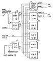
- Latches in PPL 27 are selected by combination of decoded signals on lines 41 and 42.
- the specific combination for connecting and selecting a particular latch on the modules 40 is determined from the latch selection chart of FIG. 4. As shown in the examples indicated, the position latch PPL 1 which is in the odd column 1 has the address combination XO and YO while PPL 2 in even column 4 has address combination X1 and YO. Other combinations can be determined for 132 latches (corresponding with 132 hammer operating circuits and print hammers) from the chart and examples shown.
- PPL 27 for the illustrated embodiment comprises 132 latches arranged in suitable configuration, each latch being connected to the combination of an X and Y address line from bus 26 as described and plus further connections to the FT generator 28 and RT generator 33.
- FIG. 2 shows the circuit configuration in which print position latches are grouped in modules 40 in an ODD/EVEN arrangement corresponding with the ODD/EVEN arrangement of the hammer driver cards HDC 1-6.
- Lines 41 and 42 comprise the sixteen (16) and nine (9) X and Y address lines of bus 26 as previously described.
- selection signals for the X and Y address on lines 41 and 42 to AND INVERT circuit AI 43 during RT time causes a gating signal to be applied through inverter 44 to AND circuit 45.
- the gating signal is supplied also on the feedback connection 46 to the input of AND INVERT circuit Al 47. This sets the latch and holds the gating signal at AND gate 45 until reset by an RT signal through inverter 48 to AI circuits 43 and 47.
- Fire tier signals -FT 1-5 through inverter 49 are GATED through AND circuit 45 and inverter 50 to the input of a predriver circuit which is part of the hammer operating circuit of HDC 1-6. For example: for print position PP 88 to be selected, as illustrated in FIG.
- the signals on lines 41 and 42 to AI circuit 43 would be X 8 from X decoder 36 and Y 80 from Y decoder 37.
- This combination sets the latch for gating the fire tier signal -FT 2 through AND gate 45 and inverter 50 to the predriver circuit for print position 89 on the hammer driver card HDC-5.
- FIG. 10 is a schematic showing a hammer operating circuit usable for energizing one of the coils 30 of an individual print hammer.
- the input 51 of hammer predriver 52 is connected to inverter 50 of FIG. 6 for activation as previously described.
- the output of predriver 52 is connected to the base of transistor 53 of a driver circuit which includes resistors R 1 and R 2.
- transistor 53 draws current from the + 32 V power supply through hammer coil 30 to ground.
- Terminal 54 is a connection point for the feedback to the parity circuits.
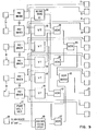
- the circuit diagram of FIG. 8 consists of four circuit modules Chip 1-4 which contain predriver and parity circuits on one of the hammer driver cards HDC 1-6. Together, Chips 1-4 have twenty-two input terminals 51-1, 51-2, 51-3 and 51-4 for twenty-two predriver circuits. Output terminals from the predriver circuits are identified by numbers 55-1, 55-2, 55-3 and 55-4 for connection to the hammer driver circuits of the type shown in FIG. 10.
- Chip 4 has parity circuits associated with predriver circuits for producing a chip parity O/E signal on line 56.
- CHIP 3 has parity circuits associated with its predriver circuits and the EXT connection to line 57.
- Chip 1 generates the chip parity O/E signal on line 58 to Chip 3.
- the parity circuits combine the O/E signal on line 58 with the predriver outputs to present the card ODD/EVEN PARITY signal at terminal 59 which is connected to the parity signal line of bus 34 of FIG. 1.
- FIG. 9 shows further details of the predriver and parity circuits for one of the modules of FIG. 8.
- the parity circuits comprise exclusive OR circuits XOR 60-64 and XOR driver circuit 65 arranged in a tree configuration.
- Voltage translators 66 connected to voltage reference 67 stabilize the voltage level of signals from the predrivers 52.
- the external O/E signal is from terminal 68 through ODD/EVEN extend circuit 69 to XOR 63.
- XOR driver 65 has an output 70 for connection to another Chip or to the ODD/EVEN PARITY line of bus 34.
- Terminal 71 and 72 provide for connection for the predrivers to hammer driver circuits as shown in FIG. 10.
- MPU 11 In preparation for printing MPU 11 precalculates an expected parity for those subscans in which print position fire data is generated for hammer operating circuits to be activated in a subscan. This is done preferably in the course of building the print position fire table PPFT in accordance with microprogramming contained in ROS 12 and operable as described in detail in the cross-referenced applications. Expected parity is computed and stored or updated and stored by MPU 11 in the last table address each time print position fire data is added to the print position fire table. For the purpose of computing expected parity a look up table is provided in ROS 12 which identifies numbers of the HDC for each print position.
- each print position is identified by one of six numbers (in the hex code 01, 02, 04, 08, 10, 20) based on the ODD/EVEN arrangement of the operating circuits on HDC 1-6.
- print position PP 2 has a hex table number 02 (for HDC-2) while PP 47 has the hex table number 04 (for HDC-3).
- MPU 11 exclusive OR's the table number for PP 47 with the expected parity for print PP 2.
- the result of the exclusive OR process would be an ODD/EVEN expected parity 06 which is stored in the last address position of the print position fire table. In this way parity checking as described hereafter relates to the hammer driver cards which are field replacable units.
- MPU 11 during the course of controlling the printing operations also performs parity checking of the hammer operating circuits and specifically the predriver circuits. This is done each subscan interval during a check parity valid window time when all operating circuits are in stable condition, i.e. no circuits are being turned ON or OFF (e.g. TO, T3, T6, T9, T12, T15 in FIG. 7). Basically, parity checking is performed by MPU 11 calculating a composite parity for each subscan and comparing it with the actual parity for a particular subscan as presented by the parity checking circuits of the hammer driver cards HDC 1-6 on bus 34 to MPXR 16.
- MPU 11 For parity checking MPU 11, or alternatively RAM 10, has a plurality of registers for storing the various parity bytes used in the computation and in the comparing operations. As seen in FIG. 11 registers A, B, C and D provide storage for the expected parity bytes from the last four subscans. NP register contains the new expected parity byte from the PPFT in RAM 10. CP is the storage register for the composite parity byte calculated by MPU 11. The PFB register is the storage for the actual parity AP received from the feedback lines of bus 34 to multiplexor MPXR 16.
- FIG. 11 shows the sequence of steps in the computation of the expected parity.
- subscan SS 1 time the contents of register A are exclusive OR'd with the contents of the CP register and stored in the CP register. At the beginning of printing both of the registers may have a zero byte so that the result is a zero.
- the expected parity byte for SS1 from the PPFT is placed in the NP register (preferably immediately following the reading of the print position data from PPFT) and exclusive OR'd with the contents of the CP register.
- the contents of NP register are then stored in the A register.
- MPU 11 then reads the actual parity from MPXR 16 by generating the multiplexor address to MPU decode 17 and through address selector 14 to MPXR 16.
- a CHIP SEL signal from MPU decode 17 gates the AP byte to the PFB register.
- MPU 11 compares the contents of the CP register and the PFB register and generate no error signal if the results of the comparison equals zero. For each succeeding subscan SS 2, SS 3, and SS 4 the process is repeated. Each time MPU 11 takes the next expected parity byte NP from the PPFT table into the NP register as described and then stores it in the B, C, or D registers respectively.
- the final contents of the CP register corresponds to the expected parity byte for all hammer operating circuits of the hammer driver cards HDC 1-6 which were expected to be turned on in the three preceding subscans plus the fourth subscan being processed from PPFT. This (when firing) should then correspond with the actual parity AP as represented by the ODD/EVEN PARITY from the parity circuits as described in FIGS. 8 and 9.
- the initial CP represents the expected parity for the preceding four subscans.
- the contents of A register, which is the expected parity for SS1, and CP are exclusive OR'd and the result stored in CP register. This corrects CP for hammers turning OFF.
- This CP is exclusive OR'd with the new NP byte for the fifth subscan and the results stored in CP register. This updates CP for hammers turning ON. NP is then stored in the A register to be used in subsequent updates.
- MPU 11 performs the composite parity calculation each subscan, the new subscan parity byte from the PPFT is added and the first of the series of subscan parity bytes is dropped. In this manner, MPU 11 is constantly updating the expected parity for comparison with the actual parity, which itself continuously changes as predrivers are activated and deactivated, thereby continuously checking the state of the hammer driver circuits over the course of the entire fire tier interval.
- each operating circuit is checked more than once during its ON and OFF time so that any conditions affecting the status or operation of the hammers occuring during that time will be reflected in one of the series of parity checks made for those operating circuits.
- the system operation can be interrupted for the purpose of performing diagnostics and for identifying the individual hammer operating circuits where the error occurred.
- the identification of the site of the error need not be more precise than identification of the hammer driver card which is a field replaceable unit FRU which can be readily removed and replaced by a . non-defective unit.
Landscapes
- Engineering & Computer Science (AREA)
- Theoretical Computer Science (AREA)
- Physics & Mathematics (AREA)
- General Engineering & Computer Science (AREA)
- General Physics & Mathematics (AREA)
- Quality & Reliability (AREA)
- Accessory Devices And Overall Control Thereof (AREA)
- Impact Printers (AREA)
Applications Claiming Priority (2)
| Application Number | Priority Date | Filing Date | Title |
|---|---|---|---|
| US06/115,841 US4335460A (en) | 1980-01-28 | 1980-01-28 | Printer system having parity checking of print hammers using software control |
| US115841 | 1980-01-28 |
Publications (2)
| Publication Number | Publication Date |
|---|---|
| EP0033067A1 EP0033067A1 (en) | 1981-08-05 |
| EP0033067B1 true EP0033067B1 (en) | 1983-04-20 |
Family
ID=22363710
Family Applications (1)
| Application Number | Title | Priority Date | Filing Date |
|---|---|---|---|
| EP81100079A Expired EP0033067B1 (en) | 1980-01-28 | 1981-01-08 | Printer system |
Country Status (7)
| Country | Link |
|---|---|
| US (1) | US4335460A (enExample) |
| EP (1) | EP0033067B1 (enExample) |
| JP (1) | JPS56114078A (enExample) |
| BR (1) | BR8100465A (enExample) |
| CA (1) | CA1159710A (enExample) |
| DE (1) | DE3160186D1 (enExample) |
| ES (1) | ES498829A0 (enExample) |
Families Citing this family (8)
| Publication number | Priority date | Publication date | Assignee | Title |
|---|---|---|---|---|
| US4317412A (en) * | 1980-06-25 | 1982-03-02 | International Business Machines Corporation | Control system and method for testing print hammers in a high speed printer |
| US4578140A (en) * | 1981-07-21 | 1986-03-25 | Teraoka Seiko Co., Ltd. | Cassette type labeler and cassette case |
| US4453251A (en) * | 1981-10-13 | 1984-06-05 | Burroughs Corporation | Error-correcting memory with low storage overhead and fast correction mechanism |
| US4425844A (en) | 1982-06-23 | 1984-01-17 | International Business Machines Corporation | Home pulse compensation for multiple speed line printer |
| US4457229A (en) * | 1982-12-27 | 1984-07-03 | International Business Machines Corporation | Scan correction for a line printer having multi-pitch type carriers |
| US5120257A (en) * | 1991-02-13 | 1992-06-09 | E. I. Du Pont De Nemours And Company | Lanced hold-downs |
| US5751744A (en) * | 1993-02-01 | 1998-05-12 | Advanced Micro Devices, Inc. | Error detection and correction circuit |
| US5411404A (en) * | 1993-10-29 | 1995-05-02 | The Whitaker Corporation | Electrical connector having bus bars providing circuit board retention |
Citations (2)
| Publication number | Priority date | Publication date | Assignee | Title |
|---|---|---|---|---|
| US3845710A (en) * | 1973-10-02 | 1974-11-05 | Teletype Corp | Print control logic circuitry for on-the-fly printers |
| US3887901A (en) * | 1974-04-29 | 1975-06-03 | Sperry Rand Corp | Longitudinal parity generator for mainframe memories |
Family Cites Families (9)
| Publication number | Priority date | Publication date | Assignee | Title |
|---|---|---|---|---|
| US2941188A (en) * | 1954-07-01 | 1960-06-14 | Rca Corp | Printer control system |
| US3140470A (en) * | 1958-08-04 | 1964-07-07 | Honeywell Regulator Co | Error checking circuit for a plurality of parallel data transmission channels |
| NL135488C (enExample) * | 1959-12-29 | |||
| US3240920A (en) * | 1961-05-29 | 1966-03-15 | Honeywell Inc | Data transmission verifier |
| US3222651A (en) * | 1961-08-02 | 1965-12-07 | Honeywell Inc | Information handling apparatus |
| US3246292A (en) * | 1961-10-04 | 1966-04-12 | Honeywell Inc | Echo check with time-phased input data sampling means |
| FR1458258A (fr) * | 1965-07-21 | 1966-03-04 | Bull General Electric | Perfectionnements aux moyens de contrôle pour vérifier le fonctionnement correct de dispositifs d'enregistrement |
| US3560926A (en) * | 1967-05-15 | 1971-02-02 | Vyzk Ustav Matemat Stroju | Error checking circuit for digitally controlled printers |
| US4008389A (en) * | 1973-09-05 | 1977-02-15 | Compagnie Honeywell Bull (Societe Anonyme) | Apparatus for checking the operation of control circuits |
-
1980
- 1980-01-28 US US06/115,841 patent/US4335460A/en not_active Expired - Lifetime
- 1980-11-21 CA CA000365265A patent/CA1159710A/en not_active Expired
- 1980-12-15 JP JP17595780A patent/JPS56114078A/ja active Granted
-
1981
- 1981-01-08 EP EP81100079A patent/EP0033067B1/en not_active Expired
- 1981-01-08 DE DE8181100079T patent/DE3160186D1/de not_active Expired
- 1981-01-27 ES ES498829A patent/ES498829A0/es active Granted
- 1981-01-28 BR BR8100465A patent/BR8100465A/pt not_active IP Right Cessation
Patent Citations (2)
| Publication number | Priority date | Publication date | Assignee | Title |
|---|---|---|---|---|
| US3845710A (en) * | 1973-10-02 | 1974-11-05 | Teletype Corp | Print control logic circuitry for on-the-fly printers |
| US3887901A (en) * | 1974-04-29 | 1975-06-03 | Sperry Rand Corp | Longitudinal parity generator for mainframe memories |
Also Published As
| Publication number | Publication date |
|---|---|
| ES8204654A1 (es) | 1982-05-16 |
| DE3160186D1 (en) | 1983-05-26 |
| US4335460A (en) | 1982-06-15 |
| ES498829A0 (es) | 1982-05-16 |
| JPS56114078A (en) | 1981-09-08 |
| EP0033067A1 (en) | 1981-08-05 |
| CA1159710A (en) | 1984-01-03 |
| BR8100465A (pt) | 1981-08-18 |
| JPS6210198B2 (enExample) | 1987-03-04 |
Similar Documents
| Publication | Publication Date | Title |
|---|---|---|
| US3771135A (en) | Remote terminal system | |
| EP0033067B1 (en) | Printer system | |
| US4291992A (en) | Printer pin control circuitry | |
| US4317412A (en) | Control system and method for testing print hammers in a high speed printer | |
| US4342096A (en) | Variable pitch character generator for dot matrix printer | |
| US4242003A (en) | Multi-pass matrix printing | |
| US6312079B1 (en) | Print head drive scheme for serial compression of I/O in ink jets | |
| EP0072224B1 (en) | A device for checking the printing circuit of a thermal printer | |
| EP0033069B1 (en) | Printer system with continuous-moving type element | |
| US3921517A (en) | Random firing of multiple width print hammers | |
| EP0098375A2 (en) | Compensation circuit for multiple speed printer | |
| EP0303124B1 (en) | Control for enabling flight timing of hammers during printing | |
| EP0033153A2 (en) | Printer system | |
| EP0145961A1 (en) | Printing apparatus | |
| US3602138A (en) | Hammer driver timing from a print buffer ring | |
| US3560926A (en) | Error checking circuit for digitally controlled printers | |
| US3323450A (en) | Fully checked electronic printing system | |
| US3171349A (en) | Output circuit for magnetic core memory in a high speed printer | |
| US4796202A (en) | Speeding mapping of print characters in a microprocessor controlled bank printer | |
| EP0121882A2 (en) | High quality printing method | |
| US4242735A (en) | Calculator-printer interface with numerical string segmentation | |
| US3936802A (en) | Control device for recording elements | |
| JPS62225373A (ja) | ラインプリンタ | |
| GB1561069A (en) | Programmmable calculator | |
| JPS6238148B2 (enExample) |
Legal Events
| Date | Code | Title | Description |
|---|---|---|---|
| PUAI | Public reference made under article 153(3) epc to a published international application that has entered the european phase |
Free format text: ORIGINAL CODE: 0009012 |
|
| AK | Designated contracting states |
Designated state(s): BE CH DE FR GB IT NL |
|
| 17P | Request for examination filed |
Effective date: 19810923 |
|
| ITF | It: translation for a ep patent filed | ||
| GRAA | (expected) grant |
Free format text: ORIGINAL CODE: 0009210 |
|
| AK | Designated contracting states |
Designated state(s): BE CH DE FR GB IT LI NL |
|
| REF | Corresponds to: |
Ref document number: 3160186 Country of ref document: DE Date of ref document: 19830526 |
|
| ET | Fr: translation filed | ||
| PG25 | Lapsed in a contracting state [announced via postgrant information from national office to epo] |
Ref country code: LI Effective date: 19840131 Ref country code: CH Effective date: 19840131 |
|
| REG | Reference to a national code |
Ref country code: CH Ref legal event code: PL |
|
| PGFP | Annual fee paid to national office [announced via postgrant information from national office to epo] |
Ref country code: GB Payment date: 19901220 Year of fee payment: 11 |
|
| PGFP | Annual fee paid to national office [announced via postgrant information from national office to epo] |
Ref country code: FR Payment date: 19901227 Year of fee payment: 11 |
|
| PGFP | Annual fee paid to national office [announced via postgrant information from national office to epo] |
Ref country code: BE Payment date: 19910114 Year of fee payment: 11 |
|
| ITTA | It: last paid annual fee | ||
| PGFP | Annual fee paid to national office [announced via postgrant information from national office to epo] |
Ref country code: NL Payment date: 19910131 Year of fee payment: 11 Ref country code: DE Payment date: 19910131 Year of fee payment: 11 |
|
| PG25 | Lapsed in a contracting state [announced via postgrant information from national office to epo] |
Ref country code: GB Effective date: 19920108 |
|
| PG25 | Lapsed in a contracting state [announced via postgrant information from national office to epo] |
Ref country code: BE Effective date: 19920131 |
|
| BERE | Be: lapsed |
Owner name: INTERNATIONAL BUSINESS MACHINES CORP. Effective date: 19920131 |
|
| PG25 | Lapsed in a contracting state [announced via postgrant information from national office to epo] |
Ref country code: NL Effective date: 19920801 |
|
| GBPC | Gb: european patent ceased through non-payment of renewal fee | ||
| NLV4 | Nl: lapsed or anulled due to non-payment of the annual fee | ||
| PG25 | Lapsed in a contracting state [announced via postgrant information from national office to epo] |
Ref country code: FR Effective date: 19920930 |
|
| PG25 | Lapsed in a contracting state [announced via postgrant information from national office to epo] |
Ref country code: DE Effective date: 19921001 |
|
| REG | Reference to a national code |
Ref country code: FR Ref legal event code: ST |
|
| PLBE | No opposition filed within time limit |
Free format text: ORIGINAL CODE: 0009261 |
|
| STAA | Information on the status of an ep patent application or granted ep patent |
Free format text: STATUS: NO OPPOSITION FILED WITHIN TIME LIMIT |