US3845710A - Print control logic circuitry for on-the-fly printers - Google Patents
Print control logic circuitry for on-the-fly printers Download PDFInfo
- Publication number
- US3845710A US3845710A US00402864A US40286473A US3845710A US 3845710 A US3845710 A US 3845710A US 00402864 A US00402864 A US 00402864A US 40286473 A US40286473 A US 40286473A US 3845710 A US3845710 A US 3845710A
- Authority
- US
- United States
- Prior art keywords
- character
- data
- circuit
- characters
- Prior art date
- Legal status (The legal status is an assumption and is not a legal conclusion. Google has not performed a legal analysis and makes no representation as to the accuracy of the status listed.)
- Expired - Lifetime
Links
Images


Classifications
-
- G—PHYSICS
- G06—COMPUTING OR CALCULATING; COUNTING
- G06K—GRAPHICAL DATA READING; PRESENTATION OF DATA; RECORD CARRIERS; HANDLING RECORD CARRIERS
- G06K15/00—Arrangements for producing a permanent visual presentation of the output data, e.g. computer output printers
- G06K15/02—Arrangements for producing a permanent visual presentation of the output data, e.g. computer output printers using printers
- G06K15/08—Arrangements for producing a permanent visual presentation of the output data, e.g. computer output printers using printers by flight printing with type font moving in the direction of the printed line, e.g. chain printers
Definitions
- each 911101111 d l may advantageously 3,289,576 12/1966 Bloom et al 101/93 c be of ldemlcal qeslgm and m q Sltlgle lnte- 3,430,210 2/1969
- Bloom et al 101/93 C be of ldemlcal qeslgm and m q Sltlgle lnte- 3,430,210 2/1969
- Foure ct 101/93 C X grated circuit ch1p preferably usmg mexpenswe MOS- 3,463,081 8/1969
- Levine l 101/93 C FETS exhibiting relatively slow switching speeds, with 3,633,496 1/1972 Kearns 101/930 no sacrifice in printer performance.
- the present invention relates to printer apparatus and, more particularly, to logic control circuitry for selectively and sequentially controlling the line printing of type characters on-the-fly in such apparatus utilizing a continuously moving, endless type carrier.
- on-the-fly printers with which the present invention is primarily concerned, are of two basic impact types.
- One type utilizes a rotating type character drum, and the other more recent, and generally preferred type, utilizes an endless type character chain or belt such as is described in Huntoon-Kearney US. Pat. No. 3,742,848, herein incorporated by reference.
- the type supporting member is constructed and positioned so as to carry one or more fonts of type characters past an array of printinducing members, such as hammers, which are selectively actuated under the control of logic circuitry at.
- an indexable imprint character receiving medium such as paper in either roll or sheet stock form.
- Endless carriers also normally have the type characters mounted thereon in such a way that they are readily replaceable individually or as an entire font.
- both multiple identical and dissimilar fonts having the same or different font lengths, mayalso be employed in endless carrier impact printers. This greatly increases the versatility of the printer for specialized printing applications.
- Such character font versatility is not possible in drum printers because the circumferentially disposed font of characters in every row must be identical.
- Ghosting- is a phenomenon which occurs as a result of a print hammer, in pressing the paper against the type character to be printed, also creating sufficient pressure to produce a slight impression on the paper of the edge of a type character adjacent to the character being printed.
- ghosting or shadow effects are particularly troublesome in drum printers because the lateral spacing of the type characters in adjacent rows on the drum must necessarily be equal to the relatively close spacing of the associated print hammers.
- the hammer logic control circuitry must be capable of temporarily storing the incoming data to be printed on a given line in a manner that will allow the sequential read out and utilization of that information only as the proper type characters on the carrier are brought into alignment with the proper hammers (aligned with the print columns) for each line to be printed.
- the logic control circuit must be capable of serially receiving encoded input data to be printed, but thereafter printing that data in a sequential rather than serial manner.
- Temporary memory storage of the input data is necessary, of course, in order that every hammer, at some point in time during the printing of each line, be aligned with and capable of effecting the printing of a character corresponding to every type characters of a given font (or fonts) passing thereby.
- suaiia time-delayed,sequential mode of hammer ac tuation will be considered with respect to one particular belt printer of the type embodied herein wherein adjacent type characters on the carrier having a spacing of 1.5 times the spacing between adjacent hammers as in the aforementioned Babler application.
- every second type character may be brought into registry with every third print hammer (and column) of an array thereof at any one time.
- the type characters are moving at a constant rate of speed past the array of hammers, it is readily seen that there are continuously changing groups of type characters and print hammers brought into alignment during each print cycle.
- each print cycle may involve the printing of from 1 to the maximum number of type characters and hammers that can be aligned at any one time during a print cycle. It thus follows that the characters and hammers involved in one print cycle normally would have no particular relationship with the type characters and hammers involved in any other of the print cycles required to complete the printing of a given line.
- the logic process of successively identifying each group of characters that is sequentially brought into alignment with an associated group of hammers is referred to as a sub-scan, with three subscans constituting a scan period.
- a scan period is required to advance the type carrier by a distance equal to the spacing between two adjacent type characters.
- the spacing between hammers (or columns) being equal to only two-thirds the spacing between type characters (for a l.5 pitch relationship therebetween)
- the number of sub-scans must equal 3 X N, where N is the number of character in the font.
- the shortest possible subscan print period for any new type character-column (hammer) alignment must necessarily encompass the time required for the carrier to be displaced one half the distance between hammers (or one-third the distance between type characters). ln one illustrative embodiment, this displacement of the type carrier requires 840 microseconds.
- the logic control circuitry employed to effect highspeed impact printing on-the-fly" heretorfore has generally comprised a single storage memory having a plurality of storage locations corresponding in number to the total number of print columns of the printer. Associated with the memory typically are means for identifying the characters in the sequence in which they appear on the type carrier, means for actuating the hammers as the proper characters sequentially register therewith, means for timing the various control and print functions, and means for initiating and terminating the various electrical and mechanical operations involved in connection with the operation of the printer.
- the storage memory it has generally comprised a magnetic core arranged in a particular core plane matrix having, for example, a core plane for each bit of a chosen binary code, with each plane comprising plural cores arranged in a row and column configuration.
- a core plane matrix for example, might comprise 160 cores arranged in 16 rows of cores each so as to accommodate a corresponding number of print hammers.
- Such core memories require rather complex and expensive (from a fabrication standpoint) X-Y read-write driver circuitry, including X-Y windings, drivers, rings and switches.
- Such magnetic core matrices also often impose undesirable speed-power restrictions on the associated circuitry, as well as limitations on the size and layout of the composite control circuitry.
- MOSFETs metal-oxide-semiconductorfield-effect type
- Such a modular form of circuit construction would also have the advantage that it would be conducive to accommodating printers with a smaller or larger number of print columns, typically ranging from to 132 columns, for example, by simply adding or subtracting one or more identical circuit modules from the composite logic circuitry.
- circuit modules designed to be compatible with simple, switch-option circuitry that may be employed outside of the last of a series of modular circuit chips, for example, so as to accommodate and control the processing of print data for any number of print columns less than the predetermined number. In that way the need for any expensive, specially designed circuit chips would be obviated.
- a concomitant problem affecting both circuit speed requirements and total line printing speed in endless carrier, on-the-fly printers heretofore is related to the need to first store a complete line of data before printing commences. This has generally been true whether synchronous or asynchronous storage memories were employed, and whether the hammer-type character spacings were U16 same or different.
- each module includes a free-running, logic controlled dual line storage memory capable of selectively directing intput encoded character data into and out of either of two discrete storage areas thereof. Both areas are associated with a specific and common subgroup of hammersland print columns), but each storage area is associated with a different print line.
- dual line storage'areas in each memory advantageously allows incoming data, often received at varying rates, to be temporarily stored for subsequent printing without having to resort to a batch process technique requiring an auxiliary main storage memory, for example.
- the modular nature of the logic circuitry also has the advantage that various length print lines can easily be accommodated by simply adding or subtracting one or more of the identical data processing circuit n odules as required for a given application.
- the number of print columns chosen need not be divisable by the standard number of columns assigned to each circuit module by design. Rather, each circuit module is designed so as to be compatible with outside strapoption circuitry so as to accommodate less than the standard number of print columns. Thus, there is no need for the last circuit module of a series, for example, to be specially designed to accommodate a nonstandard number of print columns.
- circuit modules may be formed on discrete chips of identical integrated circuit design, chip size may be chosen to minimize costs of both manufacture and composite circuit assembly, while simultaneously maximizing circuit chip yield and performance.
- the sub-divided, modular construction of the hammer logic control circuitry embodied herein advantageously allows individual data processing functions to be performed at a slower rate, for a given line printing speed.
- This makes it possible to exploit the desired features and characteristics of inexpensively designed MOSFET integrated circuitry, for example, without any adverse effect on printer performance.
- the present modular logic circuitry does not necessitate the use of bi-polar active devices, or customized MOSFET devices, fabricated through special and expensive processing techniques, in order to achieve-the switching speed characteristics otherwise required in prior hammer logic control circuits for a given line printing rate.
- the hammer logic control circuitry embodied in the present invention also exhibits a number of other features and advantages relating not only to control of the printer mechanism per se, but to the control of other important operating functions, such as error character detection, conditional processing time out, data overloads, even and odd parity checks, and test mode operations.
- the control circuitry is also designed to receive Standard Serial Interface (SSI) information, with the modular data processing circuits packaged on circuit cards for ease of assembly and maintenance.
- SSI Standard Serial Interface
- the outputs from the circuit cards also advantageously drive the hammer magnets directly, which simplifies the hammer actuation circuits and the wiring thereof.
- FIG. 1 is a partially broken away perspective view of a high-speed impact printer, with some parts being omitted for the purpose of illustration, together with a simplified block diagram of the associated hammer logic control circuitry for use therewith, which embodies features in accordance with the principles of the present invention
- FIG. 2 is a simplified schematic circuit diagram generally depicting the modular nature of the composite hammer logic control circuitry
- FIG. 3 is a simplified block diagram of the major associated circuits embodied in one data processing circuit module of the composite hammer logic control circuitry;
- FIGS. 4A and 4B in block diagram form, illustrate in greater detail the nature and functions of and the interconnected relationship between, all of the major circuits embodied in one processing circuit module;
- FIG. is a more detailed block and schematic circuit diagram primarily of the logic controlled dual storage memory embodied in each of the data processing circuit modules in accordance with the principles of the present invention
- FIG. 6 is a block and schematic circuit diagram illustrating in greater detail the association of the character position and print column counters with respect to the load control circuitry disclosed only generally in block diagram form in FIG. 4B;
- FIG. 7 is a more detailed block and schematic circuit diagram primarily of the character generating portion of one of the circuit modules of the composite logic control circuitry
- FIG. 8 is a block diagram of the hammer driver circuitry, including clock and reset inputs associated therewith;
- FIGS. 9 and 10 are detailed schematic circuit diagrams of interrelated logic circuitry for controlling the selective storage and read out of data from the dual storage areas of one of the circuit module memories, and for effecting the erasing of erroneous data from the memory, respectively;
- FIG. 11 is a symbolic representation of two typical sub-scan alignment patterns at one point in time between certain print columns and type characters, having a 1.5 pitch relationship therebetween, for the first and last of seven interconnected sub circuit processing modules;
- FIG. 12 is a timing chart depicting the time duration and sequence of three sub-scans, for each of three successive print periods, relative to the time delayed hammer firings initiated in response to each associated subscan;
- FIG. 13 is a symbolic representation of the functional relationships, time-wise, between the slot positions in the position and column counters relative to the slot positions in the dual storage areas of one free-running storage memory;
- FIG. 14 is a timing chart illustrating certain printer control and data processing control signals generated during a single line printing cycle.
- the logic control circuitry embodied herein is particularly adapted for use in high speed, on-the-fly, impact printers of the type depicted in FIG. 1.
- the printer identified'generally by the reference numeral 15, is of the class that utilizes an endless type carrier 16, entrained about a pair of spaced and aligned sprockets or pulleys 17a and 17b, as described in the aforementioned Huntoon-Kearney patent.
- the pulleys are journalled by any suitable means on the frame (not shown) of the impact printer.
- the carrier 16 which may comprise a chain or a toothed timing belt, is adapted to transport a plurality of type pallets 18 (only several shown in FIG. 1) in an essentially orbital path, which is oriented so as to define upper and lower line printing courses in the areas generally defined by the numerals 22 and 23, respectively.
- Each-of the type pallets 18 has a front face portion having a type character die (not shown) secured thereto or otherwise formed as an integral part thereof.
- the pallets 18 are mounted on the carrier 16 and uniformly spaced and oriented transversely therealong by means of integral shank portions 18a that extend through suitably formed channels (not shown) formed in the carrier.
- the carrier l6 and type pallets 18, including the mounting and driving structure associated therewith reference is made to the aforementioned I-luntoon-Kearney patent.
- carrier pulleys 17a and 17b constitute idler and drive pulleys respectively.
- Driving torque is contin- PQQSIYJEJLS LQQJ he p y J2.
- targgshashaft 24 which is coupled to a primeTnH er, hereinshown as a motor 26, through a drive train designated generally by a reference numeral 27 in FIG. 1.
- the drive train includes a worm gear 28, secured to a shaft 30 of the motor 26, a gear 34, operably enmeshed with worm gear 28, and secured to one end of an elongated drive shaft 35, a worm gear 36, secured to the other end of the drive shaft 35, and a gear 38, operably enmeshed with worm gear 36.
- Gear 38 is secured to the same a za asth BPIIQYWL a clutch 58, which may be of conventional design, is mounted in juxtaposition with gear 38 so as to releaseably couple a split shaft 60 to the coextensively aligned shaft 24. Selective actuation of the clutch 58 iseffected through control signals generated by the logic control circuitry embodied herein, as will be discussed in greater detail hereinafter. Whenever the clutch 58 is operated it also supplies torque through a drive train not shown to incrementally advance a web 41, or paper on which printing is to take place in the direction shown by arrow 42, one line at a time.
- the character printing mechanism further comprises both an array of spoke-like impellers 84 (only several shown in FIG. l), and a plurality of respectively associated impactors, or print hammers, designated generally by the reference numeral 85 (only several shown).
- Each impeller 84 has a plurality of radially extending, uniformly spaced spoke-like impeller teeth or elements 84a, all of which are oriented in a common plane perpendicular to the axis of the shaft 35.
- the impellers 84 are preferably arranged in a manner as disclosed in the aforementioned copending Babler application.
- Each hammer 85 is mounted in a channel (not shown) forming part of the printer frame so as to be selectively driven along a rectilinear path, perpendicular to the web 41, between a normal, untensioned, or nonprinting position, and a printing position whereat an enlarged forward head portion 85a of each hammer is propelled against the back side of the web 22, as described in a second copending application of Egon S. Babler, Ser. No. 268,237, filed July 3, 1972.
- selective hammers must be axially aligned respectively with different type pallets 18, the latter being mounted in an array on the carrier 16, as described hereinabove.
- each interponent can be positioned in: (l) a first or vertically raised upper position, with its upper free end portion disposed in the path of movement of a then immediately adjacent impeller spokelike element 84a (for transmitting force from the aligned impeller 84 to an aligned hammer 85), in consequence of which printing occurs; or (2) a second or vertically lowered, nonprinting position, in which the upper free end portion of the interponent 92 is displaced from the path of an impeller spoke 84a.
- An inked ribbon 95 is continuously driven in one direction or the other between, and in alignment with, the array of type pallets 18 and the web 41.
- An improved ribbon spool driving, reversing and tensioning mechanism for use with a printer of the type depicted in FIG. 1 is disclosed in a copending application of A. F. Riley, Ser. No. 345,407, filed Mar.
- each electromagnet 126 when energized, serves to pivot a corresponding armature 127 such that it elevates a selected interponent 92 into the path of an oncoming impeller tooth 84a. This propels the associated] hammer against the backside of the web 41 and thereby effects the printing of a character.
- the arrnatures 127 are preferably arranged in accordance with a fourth copending Babler application, Serial No. 292,003,
- the electromagnets are also preferably constructed, arranged, and energized through physical circuit connections in the manner described in the commonly assigned copending application of James F. Kearney, Ser. No. 290,192, filed-Sept. 18, 1972, now U.S. Patent 3,785,283, and herein incorporated by reference.
- a unique and improved composite hammer logic control circuit identified generally by the reference numeral 130, is employed for sequentially energizing the hammer associated electromagnets 126 at the proper times, with respect to desired type character registration, in order to effect the printing of stored characters along each successive print line sequentially, but ultimately positioned in the serial order in which they were initially received.
- the hammer logic control circuitry 130 described and claimed herein produces type character-associated control signals, relative to selected column positions, that may be employed to actuate any type of print-inducing means, whether of the solenoid or magnet-driven hammer type, or of the nonhammer type, wherein selectively pulsed magnetic fields, for example, are utilized to inductively impact magnetic type characters mounted on a nonmagnetic carrier, or disk, against a print medium.
- CARRIER CONTROLLED TIMING CIRCUIT FOR COMPOSITE LOGIC CIRCUITRY transducer 132 shown only symbolically, the basic timing signals, designated herein as a TYPE CARRIER ADVANCE (TCA) and a TYPE CARRIER AD- VANCE THREE (TCA-3) are generated to synchronize movement of the type carrier 16 relative to the firing times of selected ones of the array of hammers 85.
- TCA TYPE CARRIER ADVANCE
- TCA-3 TYPE CARRIER AD- VANCE THREE
- Each TCA pulse senses when a new type carrier-print column alignment has occured, and conditions the logic circuitry to start a new process cycle. Three TCA pulses occur while the type carrier moves the distance between two adjacent type pallets 18 (0.150 inch in one embodiment). Stated another way, a single TCA pulse occurs each time a type pallet has moved a third of the distance between adjacent type pallets, which corresponds to each possible printing instant as described in the Babler application Ser. No. 268,236.
- Each type carrier generated TCA pulse is thus employed to provide an indication to the hammer logic circuitry 130 (FIG. 1) that there is a new alignment of font. type characters and print columns of the printer.
- Each TCA-3 pulse is normally generated during every third TCA pulse time slot and when it is missing from its customary third slot position, this provides an indication to the logic circuit that the first type character of a given font on the carrier is aligned with the first, or some other chosen print column position of the printer.
- a TYPE CHAR- ACTER RESET (TCR) pulse is then generated and indicates that the first type character of a font on the carrier 16 (represented by a 0, for example), aligns with the first (or some other reference) col-- umn position of the printer.
- an I/O controller 134 essentially functions as a buffer between a conventional Standard Serial Interface (SSI) and the composite hammer logic control circuit,
- the logic control circuitry employs seven of such circuit modules 135 (only the first 135a andlast 135g being shown in FIG. 2), with each of the first six performing the necessary logic and data processing functions to effect the desired printing along twelve respectively associated columns of an eighty column printer. This, of course, results in the seventh subcircuit module 135g being associated with only the last eight columns constituting a print line.
- each circuit module 135 can be readily constructed to process the necessary print data and control the firing of either a larger or a smaller number of print hammers, and that there is no limit on the number of circuit modules that may be utilized in the interconnected manner depicted in FIG. 2.
- each of the circuit modules 135 has a number of control leads connected to the input/output (I/O) controller 134, whichmay be of conventional design.
- the purpose of the controller is to receive incoming encoded data to be printed, such as from the aforementioned conventional Standard Serial Interface (SSI), and to transform that data into the desired binary encoded form, including the necessary control information to operate the printer mechanism.
- SSI Standard Serial Interface
- the input data to be processed for printing when of a common format known as the American Standard Code for Information Interchange (ASCII), for example, wherein the binary numbers 1 throughj32 constitute special commands for non-printable characters, and the numbers 33 through 126 constituted printable character data, is changed into a format of weighted binary order so as to be com patible with the logic circuitry embodied herein.
- ASCII American Standard Code for Information Interchange
- This data is received by and transmitted from the I/O controller 134, as depicted in FIG. 2, over a four wire (double twisted pairs) input/output connection designated generally by the reference numeral 141, from a conventional parallel interface 142, which serves no part of the present invention and, thus, is shown only symbolically.
- the data transmitted over the two twisted pairs of leads 141 is accomplished, for example, by switching the operating signal currents, between voltage levels of O and 5 volts DC, supplied from a voltage source (not shown).
- a conventional differential receiver (not shown) in the I/O controller 134 may be used to detect the resulting voltage shifts.
- all print data i.e., ASCII print data and message control characters
- the logic control circuitry 130 in the form of an 18-bit word, with such data being transmitted serially at 56 k baud. Only control information is sent from the printer to the I/O controller 134.
- the most significant nonprintable command signals comprise the TYPE CARRIER ADVANCE (TCA) sync lead 163, TYPE CARRIER RESET (TCR) sync lead 165, END OF LINE (EOL) lead 168, LINE FEED lead 169, REQUEST NEXT CHARACTER (RNC) lead 172, INITIALIZE lead 174, and EMPTY lead 176.
- TCA TYPE CARRIER ADVANCE
- TCR TYPE CARRIER RESET
- EOL LINE FEED lead
- RNC REQUEST NEXT CHARACTER
- INITIALIZE lead 174 INITIALIZE lead 174
- EMPTY lead 176 EMPTY lead 176.
- the EOL lead 168 actually includes what essentially constitutes a common OR-buss on which EOL signals may be sent from the [/0 controller 134 or from circuit module 135g to all other circuit modules 135, under specified circumstances.
- the LINE FEED lead 169 also includes what essentially constitutes an AND-buss, in that all of the circuit modules must send a LINE FEED signal (l) to the I/O controller before the latter, after a specified time duration, forces the bus to a NO LINE FEED state (0). The circuit modules 135 then detect this latter state and release the LINE FEED lead 169. The significance of all of the control signals will be described in greater detail hereinafter.
- the printable character data is transmitted over Serial Data lead 181, and generally comprises encoded alphanumeric characters, punctuation marks, etc.
- a given circuit module 135 accepts coded input data to be printed only if the immediately preceding circuit module has the proper 12 column storage area full, and if its own proper 12 column memory storage area is not full. This, of course, does not mean that there has to be a printing character stored in every slot position of a merals 205a and 205g in FIG. 2.
- a PREV CKT FULL STATUS signal is shown only symbolically in FIG. 2 by leads 197a and g within the outline of the first and seventh circuit modules 135a and g.
- the OWN CKT FULL STATUS signal is similarly only shown symbolically by leads 199a and g in the same circuit modules.
- the logic circuits for these signals and their significance will be described in greater detail in connection with a description of the composite hammer logic circuitry depicted in FIGS. 3-10.
- a signal lead 201 connects each successive circuit module to the next, and actually comprises an extension of the TCR lead 165 depicted in FIG. 2.
- the lead 201 actually interconnects successive modules 135, it is shown symbolically in FIG. 2 as having both an output portion 201" and an input portion 201'.
- two different encoded signals are multiplexed on the intercoupling lead 201, one signal comprises OWN CKT FULL STATUS information with respect to a particular preceding adjacent one of the circuit modules 135b-g (excluding 135a and the other signal comprises TYPE CARRIER RESET (TCR) information.
- the TYPE CARRIER RESET (TCR) information is shifted into and out of each of the seven circuit modules 135a-g in succession.
- the TCR signal trans- 'mitted over the lead 201 is actually shifted through an eight element shift register 261 (not shown in FIG. 2, but described below in connection with FIGS. 3 and 4), at a rate corresponding to the periodic alignment of type characters with print column positions (or hammers) of the printer.
- the generation of the LINE FEED (lead 169) and EOL (lead 168) signals between the I/O controller and circuit modules controls the processingof each new line Y of binary encoded information, and the ultimate printing of the characters represented thereby. 7
- each circuit module 135 produces a maximum of 12 possible output print signals for respectively driving directly, and selectively, 12 hammers 85 (FIG. 1), or any other type of print-inducing means, out of the total array thereof, which total is equal to the number of print columns of the printer.
- 12 hammers 85 FIG. 1
- These signals are respectively sent over 12 output leads designated generally by the reference nu- A plurality of printersignal control leads, forming a part of a cable 210 in FIG. 2, also interconnect the I/O controller 134 with the printer.
- Such printer control leads transmit the necessary control signals to effect, or provide information of, by way of example, the following printer conditions: forms versus roll paper, single versus double line feed, low paper, paper out, local line feed versus form feed, end of forms, line feed magnet energization, and motor on/off.
- These signals are normally not binary encoded and may be generated as simple voltage level changes in a conventional manner and, thus, will not be considered in further detail herein.
- the previously mentioned TCA and TCA-3 signals, produced for carrier hammer synchronization, are also transmitted between the I/O controller 134 and the transducer 132, associated with the printer carrier 16, over separate leads in the group forming the cable 210 in FIG. 2.
- the type carrier has 192 type pallets mounted within a corresponding number of slots spaced equidistant therealong, whereas in i a printing character (although it is assigned a type pallet slot), the type pallet for a predetermined ERROR symbol is inserted in that slot.
- ERROR pallet also identifies the particular font set, if two are employed, by means of two peculiar alpha characters, for example, formed on the face of the type pallet in question.
- fonts When two or more fonts are employed, they may be of equal or different lengths, with each being repeated as often as is required in order to completely fill the slots in the type carrier 16. As each of the character fonts, as previously mentioned, must begin with a SPACE, all of the characters of the shorter font are necessarily contained in the longer font.
- the 64 (including SPACE) and 96 (including SPACE and DE- LETE) character fonts are most commonly used, as three fonts of the former and two of the latter will evenly fill the 192 pallet slots in the carrier of an 80 column printer. To fit a 64 character font on the carrier for a I32 column printer of the type embodied herein, four complete, fonts plus the first 32 characters of a fifth font would be required to fill the 288 slots in the carrier with pallet-characters.
- FIG. 3 discloses in simplified form the basic hammer logic circuitry as embodied in just one of the essentially identical data processing circuit modules l35a-g depicted only symbolically in FIG. 2. A more detailed description of the circuitry and of the various functions thereof will be described in connection with a discussion of FIGS. 4-10 hereinbelow.
- the print data initially is typically received in preferably converted ASCII data format from the output of the I/O controller 134 in serial format, and then supplied through a shift register 220 to a dual storage freerunning memory 221.
- the memory is effectively sub-divided. into two distinct l2
Landscapes
- Engineering & Computer Science (AREA)
- General Engineering & Computer Science (AREA)
- Physics & Mathematics (AREA)
- General Physics & Mathematics (AREA)
- Theoretical Computer Science (AREA)
- Record Information Processing For Printing (AREA)
Abstract
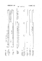
Print control logic circuitry for use in high speed ''''on-thefly'''' impact printers, wherein at least one, but preferably a plurality of independent, but interconnected data processing circuit modules, each including a separate free-running memory with logic controlled dual line storage areas, effects sequential character printing in a given line as the print data is being received, and simultaneous therewith allows for the temporary storage of print data for the next adjacent line, when required. Through the utilization of modular construction, each circuit module may advantageously be of identical design, and formed on a single integrated circuit chip, preferably using inexpensive MOSFET''S exhibiting relatively slow switching speeds, with no sacrifice in printer performance.
Description
United States Patent Brodrueck Nov. 5, 1974 Primary Examiner-Robert E. Pulfrey Assistant Examiner-Edward M. Coven [75] Inventor: Rletlef A. Brodrueck, Northbrook, Attorney, Agem r Firm K R. Bergum; J. L Lundis [73] Assignee: Teletype Corporation, Skokie, Ill. [57] ABSTRACT [22] Filed: Oct. 2, 1973 Print c ontrol logic circuitry for use in high speed on-the-fly impact printers, wherein at least one, but [21] Appl 402864 preferably a plurality of independent, but interconnected data processing circuit modules, each including [52] US. Cl.. l/93. 1fl 30/ 1l2,5 a separate free-running memorywith logic controlled [51] Int. Cl B41j 7/08 dual line storage areas, effects sequential character [58] Field of Search 101/93 C; 340/1725 printing in a given line as the print data is being reeeived, and simultaneous therewith allows for the tem- [56] References Cited porary storage of print data for the next adjacent line, UNITED STATES PATENTS when required. Through the utilization of modular 2,993,437 7/1961 Demer et al. 101 93 0 90115990901}, each 911101111 d l may advantageously 3,289,576 12/1966 Bloom et al 101/93 c be of ldemlcal qeslgm and m q Sltlgle lnte- 3,430,210 2/1969 Foure ct 101/93 C X grated circuit ch1p, preferably usmg mexpenswe MOS- 3,463,081 8/1969 Levine l 101/93 C FETS exhibiting relatively slow switching speeds, with 3,633,496 1/1972 Kearns 101/930 no sacrifice in printer performance. 3,728,688 4/1973 Elmhurst et al 101/93 C X 3,732,408 5/1973 Bettin 101 93 c x Claims, 15 Drawing Figures PROCESS CKTS MAX +0 w 11- CHAR y H BITS $20311 L\ 1 1 EMPTY I76 /74 :72039 v H INITIALIZE RNc W2 SERIAL DATA 28119 H TcA sYNcl ll lo 11 LAST CKT I63 LAST v V H i 5 Li1L ;l L 1 .L 9 L 1! I350 I F1RsT PROCESS CKT '1 1 I 1 LAST RRocEss CKT H u 3440 *1 [TYRE cARR1ER oATA 1 ,NPUT TCR1SYNC) LOGIC FOR 20/" LOGlC FOR "7 H I65 I 12 COLS 1 6 H H L11 OUTPU 1970 I J 3449 1 PRTHOTER t CONTROLLER PREV CKT PREV CKT 1 -f I FULL STATUS 1 FULL S ATUS 11 ,E OWN CKT I EOL OWN CKT i H 1|UNE FEED FULL sTATUs LINE FEED FULL STATUS 1 I69 MAGNET OR1vERs L 1| 1 3/59 F 1| 11 L H 831 INTERFACE 1 20 TO N \PARALLEL L12 /PR1NT v INTERFACE MAGNETS 1 ONE PER COLUMN H PATENTEUNM 51974 3845710 SHEET 01 [IF 12 HAMMER LOGIC TYPE CHAR. ADV PULSES PRINT CONTROL LOGIC CIRCUITRY FOR ON-TI-IE-FLY PRINTERS BACKGROUND OF THE INVENTION 1. Field of the lnvention The present invention relates to printer apparatus and, more particularly, to logic control circuitry for selectively and sequentially controlling the line printing of type characters on-the-fly in such apparatus utilizing a continuously moving, endless type carrier.
2. Description of the Prior Art So-called on-the-fly printers, with which the present invention is primarily concerned, are of two basic impact types. One type utilizes a rotating type character drum, and the other more recent, and generally preferred type, utilizes an endless type character chain or belt such as is described in Huntoon-Kearney US. Pat. No. 3,742,848, herein incorporated by reference.
ln all of these versions, the type supporting member is constructed and positioned so as to carry one or more fonts of type characters past an array of printinducing members, such as hammers, which are selectively actuated under the control of logic circuitry at.
the proper times, so as to effect the printing of the desired characters at the proper positions alongsuccessive print lines of an indexable imprint character receiving medium, such as paper in either roll or sheet stock form.
One significant advantage of the belt or chain type printer over the drum printer is that the two former versions do not present troublesome problems with respect to vertical registration of the printed characters (i.e., accurate alignment of the printed characters with respect to a horizontal reference line). In drum printers vertical registration is critically dependent on the timing of hammer actuation as the characters pass vertically thereby. This problem is essentially obviated in an endless carrier printer because both the carrier and the array of hammers are juxtaposed in accurate parallel,
horizontal relationship across the width dimension of the paper.
Endless carriers also normally have the type characters mounted thereon in such a way that they are readily replaceable individually or as an entire font. In addition, both multiple identical and dissimilar fonts, having the same or different font lengths, mayalso be employed in endless carrier impact printers. This greatly increases the versatility of the printer for specialized printing applications. Such character font versatility is not possible in drum printers because the circumferentially disposed font of characters in every row must be identical.
ln addition, as an endless type carrier allows the utilization of a wider spacing between type characters than between hammers, referred to herein as a pitch relationship therebetween, the so-called problem of ghosting may be readily eliminated. Such a type characterhammer relationship is described in the com monly assigned copending application of Egon S. Babler, Ser. No. 268,236, now US. Patent 3,795,187, herein incorporated by reference. Ghosting- (or shadow printing) is a phenomenon which occurs as a result of a print hammer, in pressing the paper against the type character to be printed, also creating sufficient pressure to produce a slight impression on the paper of the edge of a type character adjacent to the character being printed. Such ghosting or shadow effects are particularly troublesome in drum printers because the lateral spacing of the type characters in adjacent rows on the drum must necessarily be equal to the relatively close spacing of the associated print hammers.
Accordingly, while chain or belt type printers afford a number of significant advantages over the drum printer, this does not mean that there are no serious problems involved in obtaining precise control over type character-hammer registry while the former is moving on-the-fly. Such registry is very important, of course, if printed character impressions areto be not only uniformly spaced, but to exhibit distinct, sharp character line formations as required for esthetically pleasing and easily read copy.
Compounding the timing problems involved in endless type carrier printers is the fact that with the spacing between adjacent type characters normally being purposely chosen to be greater than the spacing that exists between adjacent hammers, it becomes readily apparent that at any given point in time during a print cycle, only a fractional number of the hammers will simultaneously be in exact registry with an equal number of type characters; preferably every third hammer as described in the above-cited Babler application. As such,
the hammer logic control circuitry must be capable of temporarily storing the incoming data to be printed on a given line in a manner that will allow the sequential read out and utilization of that information only as the proper type characters on the carrier are brought into alignment with the proper hammers (aligned with the print columns) for each line to be printed.
Thus, the logic control circuit must be capable of serially receiving encoded input data to be printed, but thereafter printing that data in a sequential rather than serial manner. Temporary memory storage of the input data is necessary, of course, in order that every hammer, at some point in time during the printing of each line, be aligned with and capable of effecting the printing of a character corresponding to every type characters of a given font (or fonts) passing thereby.
suaiia time-delayed,sequential mode of hammer ac tuation, and the need therefor, will be considered with respect to one particular belt printer of the type embodied herein wherein adjacent type characters on the carrier having a spacing of 1.5 times the spacing between adjacent hammers as in the aforementioned Babler application. As such, every second type character may be brought into registry with every third print hammer (and column) of an array thereof at any one time. Inasmuch as the type characters are moving at a constant rate of speed past the array of hammers, it is readily seen that there are continuously changing groups of type characters and print hammers brought into alignment during each print cycle. Thus, it can be readily seen that when there are a large number of characters to be printed along a given line, each print cycle may involve the printing of from 1 to the maximum number of type characters and hammers that can be aligned at any one time during a print cycle. It thus follows that the characters and hammers involved in one print cycle normally would have no particular relationship with the type characters and hammers involved in any other of the print cycles required to complete the printing of a given line.
As described herein, the logic process of successively identifying each group of characters that is sequentially brought into alignment with an associated group of hammers is referred to as a sub-scan, with three subscans constituting a scan period. A scan period is required to advance the type carrier by a distance equal to the spacing between two adjacent type characters. With the spacing between hammers (or columns) being equal to only two-thirds the spacing between type characters (for a l.5 pitch relationship therebetween), it is seen that in order to print any given character of a font in any one of the column positions of the printer, the number of sub-scans must equal 3 X N, where N is the number of character in the font.
It also logically follows that the shortest possible subscan print period for any new type character-column (hammer) alignment must necessarily encompass the time required for the carrier to be displaced one half the distance between hammers (or one-third the distance between type characters). ln one illustrative embodiment, this displacement of the type carrier requires 840 microseconds.
The logic control circuitry employed to effect highspeed impact printing on-the-fly" heretorfore has generally comprised a single storage memory having a plurality of storage locations corresponding in number to the total number of print columns of the printer. Associated with the memory typically are means for identifying the characters in the sequence in which they appear on the type carrier, means for actuating the hammers as the proper characters sequentially register therewith, means for timing the various control and print functions, and means for initiating and terminating the various electrical and mechanical operations involved in connection with the operation of the printer.
With respect to the storage memory, it has generally comprised a magnetic core arranged in a particular core plane matrix having, for example, a core plane for each bit of a chosen binary code, with each plane comprising plural cores arranged in a row and column configuration. Such a core plane matrix, for example, might comprise 160 cores arranged in 16 rows of cores each so as to accommodate a corresponding number of print hammers.
Disadvantageously, such core memories require rather complex and expensive (from a fabrication standpoint) X-Y read-write driver circuitry, including X-Y windings, drivers, rings and switches. Such magnetic core matrices also often impose undesirable speed-power restrictions on the associated circuitry, as well as limitations on the size and layout of the composite control circuitry.
More recently, advancements in solid state technology have resulted in very versatile and multi-faceted integrated circuitry referred to as medium or large s ca 1e irTte g ration MSl or LSl). Particularly in apfiications where very high switching speeds have not been required, the active devices in such circuitry have increasingly been of the metal-oxide-semiconductorfield-effect type, hereinafter generally referred to as MOSFETs. Such devices have proven to be very effective, reliable, and readily amenable to high volume, low cost manufacture, even in rather complex, high density MSl or LSl circuitry. To that end, MOSFETs are gaining wide acceptance for use in the fabrication of diverse logic circuitry, including gates, inverters, flipflops, counters, shift registers, and the like.
With respect to printer logic control circuitry, however, all of the required circuit logic cannot at present, at least, be economically fabricated on a single semiconductor chip. This has thus necessitated a number of different logic circuit chips heretofore, with rather complex and extensive interfacing being required therebetween in order to assemble a composite printer hammer logic control circuit. This, of course, does not lead to low cost, high yield composite circuits that would be possible if every circuit chip could be of identical construction, be capable of independently processing print data for only an assigned subgroup of print columns, and be interconnected in a simple, modular fashion so as to constitute the complete logic circuitry for an 80 column printer, for example.
Such a modular form of circuit construction would also have the advantage that it would be conducive to accommodating printers with a smaller or larger number of print columns, typically ranging from to 132 columns, for example, by simply adding or subtracting one or more identical circuit modules from the composite logic circuitry. Unfortunately, with most hammer logic control circuits employed heretofore, the maximum number of print columns that can normally be controlled is fixed by unalterable circuit parameters.
Accordingly, there exists a definite need for a modular constructed hammer logic control circuit, particularly wherein the number of print columns chosen forany given application need not be divisable by any given number of identical circuit modules, each of which may be designed normally to accommodate and control the processing of print data for a given predetermined number of print columns. To that end, what is needed is circuit modules designed to be compatible with simple, switch-option circuitry that may be employed outside of the last of a series of modular circuit chips, for example, so as to accommodate and control the processing of print data for any number of print columns less than the predetermined number. In that way the need for any expensive, specially designed circuit chips would be obviated.
A concomitant problem affecting both circuit speed requirements and total line printing speed in endless carrier, on-the-fly printers heretofore is related to the need to first store a complete line of data before printing commences. This has generally been true whether synchronous or asynchronous storage memories were employed, and whether the hammer-type character spacings were U16 same or different.
It is thus seen that there is a need for hammer logic control circuitry for on-the-fly belt printers that can fully exploit the many advantages of MOSFET circuitry, without requiring a cost-performance trade-off in the logic circuitry in order to attain the high speed printing rates desired.
5 SUMMARY OF THE INVENTION It, therefore, is an object of the present invention to provide new and improved type character selection and print logic control circuitry for use in on-the-fly high speed printer apparatus.
It is a further object of the present invention to utilize the virtues of MOSFET integrated circuitry in on-the fly printer apparatus in a manner that allows reliable, simplified, low cost fabrication thereof, through the use of selective, logic controlled, dual line character storage read out of the information to be printed.
In accordance with the principles of the present invention, these and other objects are accomplished through the utilization of a plurality of intercoupled, but independently operated data processing circuit modules. Each module includes a free-running, logic controlled dual line storage memory capable of selectively directing intput encoded character data into and out of either of two discrete storage areas thereof. Both areas are associated with a specific and common subgroup of hammersland print columns), but each storage area is associated with a different print line. Such dual line storage'areas in each memory advantageously allows incoming data, often received at varying rates, to be temporarily stored for subsequent printing without having to resort to a batch process technique requiring an auxiliary main storage memory, for example.
The utilization of multiple data processing circuit modules, with each associated with a different sub group of print hammers (and columns), advantageously allows the switching speeds of the various active integrated circuit elements embodied in each processing circuit to be lower, for a given line printing speed, than would be possible with a single-storage memory having sufficient storage for all of the character data to be printed along a given line. Considered more specifically, with each circuit module controlling only a fractional number of the total print hammers employed in a given printer, the number of storage positions in the memory thereof are likewise reduced. Accordingly, the scanning .(or read out) rate of the circuit can be reduced, as the limited number of encoded characters stored may be processed and printed independently of, but concurrently with the input data received in and processed by the other circuit modules.
In contrast, with a typical single shift register type of memory employed heretofore, if there are 80 columns of possible data to be stored for subsequent printing along a given line, for example, then that data must normally be shifted through 80 elements of the shift register memory every time a different type character is brought into alignment with a different column and associated hammer, until all possible alignment combinations therebetween have been compared. It thus becomes readily apparent that as the number of storage positions required in the memory increase, the circuit logic switching speed of not only the memory, but of the other associated processing circuitry must also increase for a given line printing speed.
The modular nature of the logic circuitry also has the advantage that various length print lines can easily be accommodated by simply adding or subtracting one or more of the identical data processing circuit n odules as required for a given application. Moreover, in accordance with the principles of the present invention, the number of print columns chosen need not be divisable by the standard number of columns assigned to each circuit module by design. Rather, each circuit module is designed so as to be compatible with outside strapoption circuitry so as to accommodate less than the standard number of print columns. Thus, there is no need for the last circuit module of a series, for example, to be specially designed to accommodate a nonstandard number of print columns.
As all of the circuit modules may be formed on discrete chips of identical integrated circuit design, chip size may be chosen to minimize costs of both manufacture and composite circuit assembly, while simultaneously maximizing circuit chip yield and performance.
It is thus seen that the sub-divided, modular construction of the hammer logic control circuitry embodied herein advantageously allows individual data processing functions to be performed at a slower rate, for a given line printing speed. This, in turn, makes it possible to exploit the desired features and characteristics of inexpensively designed MOSFET integrated circuitry, for example, without any adverse effect on printer performance. Stated another way, the present modular logic circuitry does not necessitate the use of bi-polar active devices, or customized MOSFET devices, fabricated through special and expensive processing techniques, in order to achieve-the switching speed characteristics otherwise required in prior hammer logic control circuits for a given line printing rate.
The hammer logic control circuitry embodied in the present invention, as will be discussed in greater detail hereinbelow, also exhibits a number of other features and advantages relating not only to control of the printer mechanism per se, but to the control of other important operating functions, such as error character detection, conditional processing time out, data overloads, even and odd parity checks, and test mode operations. The control circuitry is also designed to receive Standard Serial Interface (SSI) information, with the modular data processing circuits packaged on circuit cards for ease of assembly and maintenance. The outputs from the circuit cards also advantageously drive the hammer magnets directly, which simplifies the hammer actuation circuits and the wiring thereof.
BRIEF DESCRIPTION OF THE DRAWINGS FIG. 1 is a partially broken away perspective view of a high-speed impact printer, with some parts being omitted for the purpose of illustration, together with a simplified block diagram of the associated hammer logic control circuitry for use therewith, which embodies features in accordance with the principles of the present invention;
FIG. 2 is a simplified schematic circuit diagram generally depicting the modular nature of the composite hammer logic control circuitry;
FIG. 3 is a simplified block diagram of the major associated circuits embodied in one data processing circuit module of the composite hammer logic control circuitry;
FIGS. 4A and 4B, in block diagram form, illustrate in greater detail the nature and functions of and the interconnected relationship between, all of the major circuits embodied in one processing circuit module;
FIG. is a more detailed block and schematic circuit diagram primarily of the logic controlled dual storage memory embodied in each of the data processing circuit modules in accordance with the principles of the present invention;
FIG. 6 is a block and schematic circuit diagram illustrating in greater detail the association of the character position and print column counters with respect to the load control circuitry disclosed only generally in block diagram form in FIG. 4B;
FIG. 7 is a more detailed block and schematic circuit diagram primarily of the character generating portion of one of the circuit modules of the composite logic control circuitry;
FIG. 8 is a block diagram of the hammer driver circuitry, including clock and reset inputs associated therewith;
FIGS. 9 and 10 are detailed schematic circuit diagrams of interrelated logic circuitry for controlling the selective storage and read out of data from the dual storage areas of one of the circuit module memories, and for effecting the erasing of erroneous data from the memory, respectively;
FIG. 11 is a symbolic representation of two typical sub-scan alignment patterns at one point in time between certain print columns and type characters, having a 1.5 pitch relationship therebetween, for the first and last of seven interconnected sub circuit processing modules;
FIG. 12 is a timing chart depicting the time duration and sequence of three sub-scans, for each of three successive print periods, relative to the time delayed hammer firings initiated in response to each associated subscan;
FIG. 13 is a symbolic representation of the functional relationships, time-wise, between the slot positions in the position and column counters relative to the slot positions in the dual storage areas of one free-running storage memory; and
FIG. 14 is a timing chart illustrating certain printer control and data processing control signals generated during a single line printing cycle.
DETAILED DESCRIPTION OF THE INVENTION GENERAL DESCRIPTION OF LOGIC CONTROLLED PRINTER APPARATUS The logic control circuitry embodied herein is particularly adapted for use in high speed, on-the-fly, impact printers of the type depicted in FIG. 1. As disclosed therein, the printer, identified'generally by the reference numeral 15, is of the class that utilizes an endless type carrier 16, entrained about a pair of spaced and aligned sprockets or pulleys 17a and 17b, as described in the aforementioned Huntoon-Kearney patent. The pulleys are journalled by any suitable means on the frame (not shown) of the impact printer. The carrier 16, which may comprise a chain or a toothed timing belt, is adapted to transport a plurality of type pallets 18 (only several shown in FIG. 1) in an essentially orbital path, which is oriented so as to define upper and lower line printing courses in the areas generally defined by the numerals 22 and 23, respectively.
Each-of the type pallets 18 has a front face portion havinga type character die (not shown) secured thereto or otherwise formed as an integral part thereof.
The pallets 18 are mounted on the carrier 16 and uniformly spaced and oriented transversely therealong by means of integral shank portions 18a that extend through suitably formed channels (not shown) formed in the carrier. As will presently be seen, in accordance with the present printer embodiment, there are normally at least twice as many type pallets-characters on the carrier than in any chosen font. This means that a given sequence of characters is repeated more than once along the entire length of the carrier. If desired, of course, several fonts of different lengths could also be employed for a special printing application. For further details as to one preferred embodiment of the carrier l6 and type pallets 18, including the mounting and driving structure associated therewith, reference is made to the aforementioned I-luntoon-Kearney patent.
In the illustrative embodiment of the printer depicted in FIG. 1, carrier pulleys 17a and 17b constitute idler and drive pulleys respectively. Driving torque is contin- PQQSIYJEJLS LQQJ he p y J2. targgshashaft 24 which is coupled to a primeTnH er, hereinshown as a motor 26, through a drive train designated generally by a reference numeral 27 in FIG. 1. The drive train includes a worm gear 28, secured to a shaft 30 of the motor 26, a gear 34, operably enmeshed with worm gear 28, and secured to one end of an elongated drive shaft 35, a worm gear 36, secured to the other end of the drive shaft 35, and a gear 38, operably enmeshed with worm gear 36. Gear 38 is secured to the same a za asth BPIIQYWL a clutch 58, which may be of conventional design, is mounted in juxtaposition with gear 38 so as to releaseably couple a split shaft 60 to the coextensively aligned shaft 24. Selective actuation of the clutch 58 iseffected through control signals generated by the logic control circuitry embodied herein, as will be discussed in greater detail hereinafter. Whenever the clutch 58 is operated it also supplies torque through a drive train not shown to incrementally advance a web 41, or paper on which printing is to take place in the direction shown by arrow 42, one line at a time.
For further details as to the drive trains for both the type carrier 16 and the web 41, reference is again made to the I-Iuntoon-Kearney patent.
In the illustrative impact printer embodiment depicted in FIG. 1, the character printing mechanism further comprises both an array of spoke-like impellers 84 (only several shown in FIG. l), and a plurality of respectively associated impactors, or print hammers, designated generally by the reference numeral 85 (only several shown). There is one impeller and associated hammer for each possible printing position or column across the width of the web 41, with the spaced impellers being concentrically secured to the longitudinally extending drive shaft 35. Each impeller 84 has a plurality of radially extending, uniformly spaced spoke-like impeller teeth or elements 84a, all of which are oriented in a common plane perpendicular to the axis of the shaft 35. In a preferred embodiment of the printer, the impellers 84 are preferably arranged in a manner as disclosed in the aforementioned copending Babler application.
Each hammer 85 is mounted in a channel (not shown) forming part of the printer frame so as to be selectively driven along a rectilinear path, perpendicular to the web 41, between a normal, untensioned, or nonprinting position, and a printing position whereat an enlarged forward head portion 85a of each hammer is propelled against the back side of the web 22, as described in a second copending application of Egon S. Babler, Ser. No. 268,237, filed July 3, 1972. In order to facilitate printing at any given time, it is apparent that selective hammers must be axially aligned respectively with different type pallets 18, the latter being mounted in an array on the carrier 16, as described hereinabove. As such, the continuous movement of the pallet-type character assemblies along a path extending across the width of, and closely adjacent to, the front side of the web 41, makes it possible for each pallet 18 (with a type character die'on the front face thereof), or groups thereof, tobe successfully brought into momentary axial alignment with the hammers 85.
The agency through which each impeller 84 drives an impeller 84 and hammer 85. The interponents 92 are disposed in a lateral array, extending parallel to and respectively aligned with the adjacent free rearward ends 8512 of the hammers 85. Briefly described herein, each interponent can be positioned in: (l) a first or vertically raised upper position, with its upper free end portion disposed in the path of movement of a then immediately adjacent impeller spokelike element 84a (for transmitting force from the aligned impeller 84 to an aligned hammer 85), in consequence of which printing occurs; or (2) a second or vertically lowered, nonprinting position, in which the upper free end portion of the interponent 92 is displaced from the path of an impeller spoke 84a.
The manner in which the hammers 85 are mechani'- cally driven (as distinguished from electronically controlled) against the web 41 forms no part of the present invention. For details relating to the cooperating mechanical relationship between the impellers 84, hammers 85 and interponents 92, reference is made to the three copending Babler applications previously cited.
An inked ribbon 95, as depicted in only fragmentary form in FIG. 1, is continuously driven in one direction or the other between, and in alignment with, the array of type pallets 18 and the web 41. One preferred embodiment of an improved ribbon spool driving, reversing and tensioning mechanism for use with a printer of the type depicted in FIG. 1 is disclosed in a copending application of A. F. Riley, Ser. No. 345,407, filed Mar.
. 27, 1973, also assigned to the assignee of the present LII printer 15, as thus ,far described, constitutes a line- I at-a-time printer, i.e., a plurality of characters are normally sequentially printed across the width dimension of the web 41 during each of a plurality of print cycles that occur between successive index advancements of the web 41. The printing of actual images on the back or rear side of the 'web 41, as
-xie rqstiaELQj..lsisase mp shsst 9 searseby the impellers 84 generating, and. transferring through the respectively associated and selectively actuated interponents 92, sufficient force: against the respectively associated hammers 85 to cause the latter to be driven against the back side: of the web 41. The discrete hammer-propelled areas of the web 41 are then, in turn, driven against correspondingly aligned areas of the aligned inked ribbon 95, and then driven against the particular type characters on the pallets 18 aligned therewith with sufficient force to effect controlled impact printing of character images on the front side of the web 11.
The logic control circuitry required to selectively and sequentially actuate the interponent-hammer combina tions through the energization of respectively associated electromagnets 126 will now be described in greater detail. Mechanically, each electromagnet 126, when energized, serves to pivot a corresponding armature 127 such that it elevates a selected interponent 92 into the path of an oncoming impeller tooth 84a. This propels the associated] hammer against the backside of the web 41 and thereby effects the printing of a character. The arrnatures 127 are preferably arranged in accordance with a fourth copending Babler application, Serial No. 292,003,
filed September 18, 1972, now issued as US. Patent 3,805,695, herein incorporated. by reference. The electromagnets are also preferably constructed, arranged, and energized through physical circuit connections in the manner described in the commonly assigned copending application of James F. Kearney, Ser. No. 290,192, filed-Sept. 18, 1972, now U.S. Patent 3,785,283, and herein incorporated by reference.
As simply represented in block diagram form. in FIG. 1, a unique and improved composite hammer logic control circuit, identified generally by the reference numeral 130, is employed for sequentially energizing the hammer associated electromagnets 126 at the proper times, with respect to desired type character registration, in order to effect the printing of stored characters along each successive print line sequentially, but ultimately positioned in the serial order in which they were initially received. It is to be understood, of course, that the hammer logic control circuitry 130 described and claimed herein produces type character-associated control signals, relative to selected column positions, that may be employed to actuate any type of print-inducing means, whether of the solenoid or magnet-driven hammer type, or of the nonhammer type, wherein selectively pulsed magnetic fields, for example, are utilized to inductively impact magnetic type characters mounted on a nonmagnetic carrier, or disk, against a print medium.
CARRIER CONTROLLED TIMING CIRCUIT FOR COMPOSITE LOGIC CIRCUITRY transducer 132, shown only symbolically, the basic timing signals, designated herein as a TYPE CARRIER ADVANCE (TCA) and a TYPE CARRIER AD- VANCE THREE (TCA-3) are generated to synchronize movement of the type carrier 16 relative to the firing times of selected ones of the array of hammers 85.
. Precise synchronization is very important, of course, if
accurate type character-hammer registration is to be established as required for high quality printing.
Each TCA pulse senses when a new type carrier-print column alignment has occured, and conditions the logic circuitry to start a new process cycle. Three TCA pulses occur while the type carrier moves the distance between two adjacent type pallets 18 (0.150 inch in one embodiment). Stated another way, a single TCA pulse occurs each time a type pallet has moved a third of the distance between adjacent type pallets, which corresponds to each possible printing instant as described in the Babler application Ser. No. 268,236.
Each type carrier generated TCA pulse is thus employed to provide an indication to the hammer logic circuitry 130 (FIG. 1) that there is a new alignment of font. type characters and print columns of the printer. Each TCA-3 pulse is normally generated during every third TCA pulse time slot and when it is missing from its customary third slot position, this provides an indication to the logic circuit that the first type character of a given font on the carrier is aligned with the first, or some other chosen print column position of the printer. A TYPE CHAR- ACTER RESET (TCR) pulse is then generated and indicates that the first type character of a font on the carrier 16 (represented by a 0, for example), aligns with the first (or some other reference) col-- umn position of the printer.
GENERAL DESCRIPTION OF l/O CONTROLLER AND OF LOGIC CONTROL CIRCUITRY With particular reference now to FIG. 2, it is seen that an I/O controller 134 essentially functions as a buffer between a conventional Standard Serial Interface (SSI) and the composite hammer logic control circuit,
which actually comprises a plurality of essentially identical and uniquely interconnected data processing circuit modules 135. In conjunction with one illustrative 80 column printer, the logic control circuitry, in accordance with one illustrative embodiment, employs seven of such circuit modules 135 (only the first 135a andlast 135g being shown in FIG. 2), with each of the first six performing the necessary logic and data processing functions to effect the desired printing along twelve respectively associated columns of an eighty column printer. This, of course, results in the seventh subcircuit module 135g being associated with only the last eight columns constituting a print line. It is to be understood that each circuit module 135 can be readily constructed to process the necessary print data and control the firing of either a larger or a smaller number of print hammers, and that there is no limit on the number of circuit modules that may be utilized in the interconnected manner depicted in FIG. 2.
As also seen in FIG. 2, each of the circuit modules 135 has a number of control leads connected to the input/output (I/O) controller 134, whichmay be of conventional design. The purpose of the controller is to receive incoming encoded data to be printed, such as from the aforementioned conventional Standard Serial Interface (SSI), and to transform that data into the desired binary encoded form, including the necessary control information to operate the printer mechanism.
Considered more specifically, the input data to be processed for printing, when of a common format known as the American Standard Code for Information Interchange (ASCII), for example, wherein the binary numbers 1 throughj32 constitute special commands for non-printable characters, and the numbers 33 through 126 constituted printable character data, is changed into a format of weighted binary order so as to be com patible with the logic circuitry embodied herein.
This data is received by and transmitted from the I/O controller 134, as depicted in FIG. 2, over a four wire (double twisted pairs) input/output connection designated generally by the reference numeral 141, from a conventional parallel interface 142, which serves no part of the present invention and, thus, is shown only symbolically. The data transmitted over the two twisted pairs of leads 141 is accomplished, for example, by switching the operating signal currents, between voltage levels of O and 5 volts DC, supplied from a voltage source (not shown). A conventional differential receiver (not shown) in the I/O controller 134, may be used to detect the resulting voltage shifts.
In one preferred embodiment, all print data (i.e., ASCII print data and message control characters), as well as other necessary control information for the printer, is sent to the logic control circuitry 130 in the form of an 18-bit word, with such data being transmitted serially at 56 k baud. Only control information is sent from the printer to the I/O controller 134.
As depicted in FIG. 2, the most significant nonprintable command signals, identified by their respectively associated leads, comprise the TYPE CARRIER ADVANCE (TCA) sync lead 163, TYPE CARRIER RESET (TCR) sync lead 165, END OF LINE (EOL) lead 168, LINE FEED lead 169, REQUEST NEXT CHARACTER (RNC) lead 172, INITIALIZE lead 174, and EMPTY lead 176. As will be described in greater detail in connection with FIG. 10, the EOL lead 168 actually includes what essentially constitutes a common OR-buss on which EOL signals may be sent from the [/0 controller 134 or from circuit module 135g to all other circuit modules 135, under specified circumstances. Similarly, the LINE FEED lead 169 also includes what essentially constitutes an AND-buss, in that all of the circuit modules must send a LINE FEED signal (l) to the I/O controller before the latter, after a specified time duration, forces the bus to a NO LINE FEED state (0). The circuit modules 135 then detect this latter state and release the LINE FEED lead 169. The significance of all of the control signals will be described in greater detail hereinafter.
The printable character data, as distinguished from the non-printable command signals, is transmitted over Serial Data lead 181, and generally comprises encoded alphanumeric characters, punctuation marks, etc.
As is also readily seen in FIG. 2, all of the inputoutput leads of the controller 134, with the exception of the TCR lead 165, are directly connected to each of the logic circuit modules 135a-g. The TCR signal is successively passed from one sub-circuit module 135 to the next after some internal logic functions are carried out. Considered only briefly at this point, before each circuit module 135 is ready to process print data and to selectively actuate any of the proper hammers 85 associated therewith, after it has been INITIALIZED, it must have received a TCR signal and passed it through its own circuit module to the next one.
A given circuit module 135 accepts coded input data to be printed only if the immediately preceding circuit module has the proper 12 column storage area full, and if its own proper 12 column memory storage area is not full. This, of course, does not mean that there has to be a printing character stored in every slot position of a merals 205a and 205g in FIG. 2.
given storage area, as there may be one or more columns where no data is to be printed (as represented by SPACE characters), or where a character has already been printed and the memory slot therefore is empty. In such cases, the circuitry simply recognizes this fact and acts as if the memory were full.
A PREV CKT FULL STATUS signal is shown only symbolically in FIG. 2 by leads 197a and g within the outline of the first and seventh circuit modules 135a and g. The OWN CKT FULL STATUS signal is similarly only shown symbolically by leads 199a and g in the same circuit modules. The logic circuits for these signals and their significance will be described in greater detail in connection with a description of the composite hammer logic circuitry depicted in FIGS. 3-10.
A signal lead 201 connects each successive circuit module to the next, and actually comprises an extension of the TCR lead 165 depicted in FIG. 2. As the lead 201 actually interconnects successive modules 135, it is shown symbolically in FIG. 2 as having both an output portion 201" and an input portion 201'. In actual operation, two different encoded signals are multiplexed on the intercoupling lead 201, one signal comprises OWN CKT FULL STATUS information with respect to a particular preceding adjacent one of the circuit modules 135b-g (excluding 135a and the other signal comprises TYPE CARRIER RESET (TCR) information. The TYPE CARRIER RESET (TCR) information is shifted into and out of each of the seven circuit modules 135a-g in succession.
Considered more specifically, the TCR signal trans- 'mitted over the lead 201 is actually shifted through an eight element shift register 261 (not shown in FIG. 2, but described below in connection with FIGS. 3 and 4), at a rate corresponding to the periodic alignment of type characters with print column positions (or hammers) of the printer. As mentioned hereinabove, the generation of the LINE FEED (lead 169) and EOL (lead 168) signals between the I/O controller and circuit modules controls the processingof each new line Y of binary encoded information, and the ultimate printing of the characters represented thereby. 7
Two additional inputs to each circuit module 135, which are identified by leads 203a and 203g in FIG. 2,
' has a type pallet mounted therein. As a SPACE is not provide information as to the number of characters in the largest character font on the type carrier. The significance of these inputs will become more apparent hereinbelow. A
As also generally depicted in FIG. 2, each circuit module 135 produces a maximum of 12 possible output print signals for respectively driving directly, and selectively, 12 hammers 85 (FIG. 1), or any other type of print-inducing means, out of the total array thereof, which total is equal to the number of print columns of the printer. These signals are respectively sent over 12 output leads designated generally by the reference nu- A plurality of printersignal control leads, forming a part of a cable 210 in FIG. 2, also interconnect the I/O controller 134 with the printer. Such printer control leads transmit the necessary control signals to effect, or provide information of, by way of example, the following printer conditions: forms versus roll paper, single versus double line feed, low paper, paper out, local line feed versus form feed, end of forms, line feed magnet energization, and motor on/off. These signals are normally not binary encoded and may be generated as simple voltage level changes in a conventional manner and, thus, will not be considered in further detail herein. The previously mentioned TCA and TCA-3 signals, produced for carrier hammer synchronization, are also transmitted between the I/O controller 134 and the transducer 132, associated with the printer carrier 16, over separate leads in the group forming the cable 210 in FIG. 2.
Before considering the basic logic circuitry in greater detail, it is believed beneficial to describe at this point the nature of the font(s) carried by the carrier 16, as well as the manner in which they are positioned on the type pallets 18 in two illustrative impact printers. In an column printer, for example, the type carrier has 192 type pallets mounted within a corresponding number of slots spaced equidistant therealong, whereas in i a printing character (although it is assigned a type pallet slot), the type pallet for a predetermined ERROR symbol is inserted in that slot. This. ERROR pallet also identifies the particular font set, if two are employed, by means of two peculiar alpha characters, for example, formed on the face of the type pallet in question.
When two or more fonts are employed, they may be of equal or different lengths, with each being repeated as often as is required in order to completely fill the slots in the type carrier 16. As each of the character fonts, as previously mentioned, must begin with a SPACE, all of the characters of the shorter font are necessarily contained in the longer font. The 64 (including SPACE) and 96 (including SPACE and DE- LETE) character fonts are most commonly used, as three fonts of the former and two of the latter will evenly fill the 192 pallet slots in the carrier of an 80 column printer. To fit a 64 character font on the carrier for a I32 column printer of the type embodied herein, four complete, fonts plus the first 32 characters of a fifth font would be required to fill the 288 slots in the carrier with pallet-characters.
OVERVIEW OF INDIVIDUAL CIRCUITS FORMING ONE COMPLETE CIRCUIT MODULE Attention is now directed to FIG. 3, which discloses in simplified form the basic hammer logic circuitry as embodied in just one of the essentially identical data processing circuit modules l35a-g depicted only symbolically in FIG. 2. A more detailed description of the circuitry and of the various functions thereof will be described in connection with a discussion of FIGS. 4-10 hereinbelow. A A
Starting at the point of data entry in FIG. 3, the print data initially is typically received in preferably converted ASCII data format from the output of the I/O controller 134 in serial format, and then supplied through a shift register 220 to a dual storage freerunning memory 221. As previously mentioned, the memory is effectively sub-divided. into two distinct l2
Claims (29)
1. A print control logic circuit for use in high speed on-thefly printers, for selectively actuating one or more out of a plurality of character print-inducing members whenever selective type characters forming a part of a continuously moving font of type characters are momentarily brought into respectively aligned and juxtaposed relationship with said print-inducing members so as to effect sequential printing of type character images along each successive line on a medium, but with the character images ultimately being positioned in the serial order in which the input data characters to be printed were received, said logic control circuit comprising: sub-dividable memory means for storing input binary encoded data representative of the characters to be printed at particular positions along a given print line, said memory means having at least two logic controlled and operationally distinct storage areas, and including means for selectively storing input character data in and reading said data out of said storage areas in a manner that allows incoming data intended for printing on one line to be stored in one of said distinct storage areas while any previously received data is still being read out of the other storage area, processed and printed in the preceding line, means for generating type character font data in multiple phase sequences during each print cycle, said data being representative of and identifying the particular ones of said moving font type characters that are respectively brought into registry with associated ones of said character print-inducing members at any particular point in time during each phase sequence, and means for processing any stored character data for printing after having been read out of said memory means, by comparing said stored data with said generated type character data, and for generating a distinct print signal, in response to each valid equal signal comparison, for use in actuating at the proper time the particular one of an associated character print-inducing member that will effect the printing of a character image representative of the compared type character at the proper position along a given print line.
2. A print control logic circuit in accordance with claim 1 wherein said memory means includes a free-running memory, and phase controlled type character position and print column counter means for logically controlling access to and sub-dividing said memory into distinct dual storage areas.
3. A print control logic circuit in accordance with claim 1 wherein said circuit is sub-divided into a plurality of essentially identical, but interconnected data processing circuit modules, each circuit module including separate ones of said memory means, character generating means and comparing means, and with each circuit module being assigned to process print data for a pre-determined number of print columns forming only a sub-group out of the total number of print columns defining the length of a given print line, with each circuit module thereby storing, processing and effecting the printing of input data characters as received in only the print columns assigned thereto. 4. A print control logic circuit in accordance with claim 2 wherein said memory means further includes memory recovery circuit means for detecting the presence of and effecting both the erasing of any invalid data characters stored in said memory during the printing of each print line, and the printing of error symbols therefore.
5. A print control logic circuit in accordance with claim 2 wherein said memory means further includes: presettable strap-option circuit means coupled to said associated memory for detecting the presence of and purging said memory of any invalid data characters stored therein whenever such characters represent an encoded binary number higher than a preset number representative of the highest order character in a chosen font of type characters employed in a given application.
6. A print control logic circuit in accordance with claim 5 further comprising: an auxiliary invalid character recovery circuit associated with said memory means and being capable of detecting any invalid data characters stored in said memory means, and for optionally erasing said invalid characters independently of said strap-option circuit means, regardless of the length of a given character font employed in conjunction therewith, after a predetermined time delay that is chosen to be greater than the time required for the number of different type character fonts employed to successively pass a given reference point of the printer, and for thereafter causing each equal character-signal comparison representative of an invalid data character to effect the actuation of the proper print-inducing member at the proper time when an error symbol character included in a given font of type characters is momentarily brought into register therewith and, thereby, effect the printing of an error symbol.
7. A print control logic circuit in accordance with claim 3 wherein said memory means of each of said circuit modules further includes means for selectively generating first and second storage signals and first and second processing signals for controlling the loading of encoded data characters in and the readout thereof from the first and second storage areas of said memory means in a selective manner.
8. A print control logic circuit in accordance with claim 7 wherein the generated storage and processing signals are associated with the same storage areas of the memory means unless input data characters are received for storage after one storage area of said memory means has been filled, but the processing and printing of that data has not been completed.
9. A print control logic circuit in accordance with claim 3 wherein each of said memory means includes a free-running storage memory and phase-controlled type character position and print column counter means for logically controlling selective access to and sub-dividing said memory into dual storage areas, and wherein each of said circuit modules further comprises: memory recovery circuit means for detecting the presence of and effecting the erasing of any invalid data characters stored in said associated memory during the printing of each print line, and for effecting the printing of error symbols therefor.
10. A print control logic circuit in accordance with claim 9 wherein each of said circuit modules further comprises: circuit means for generating line stacking control signals for over-riding the normal operation of said associated memory so as to allow character data received at a rate faster than the printer can print the data stored in a first storage area of said memory, for a given line, to be temporarily stored in the second of said storage areas for not only the adjacent print line, but for any succeeding line thereafter until said second storage area has been filled, subject to any data for any line after the adjacent line, having not been previously transferred to said first storage area in the normal manner upon the processing and printing of the previously stored character data therein having been completed.
11. A print control logic circuit in accordance with claim 9 wherein said memory recovery circuit means in each of said circuit modules comprises presettable strap-option circuit means coupled to said associated memory for detecting the presence of and purging said memory of any invalid data characters stored therein whenever such characters represent an encoded binary number higher than a preset number representative of the highest order character in a chosen font of type characters employed in a given application.
12. A print control logic circuit in accordance with claim 11 wherein each of said circuit modules further comprises: an auxiliary invalid character recovery circuit capable of detecting any invalid data characters stored in said associated memory, and for erasing said invalid characters independently of said strap-option circuit means, regardless of the length of a given character font employed in conjunction therewith, after a predetermined time-delay that is chosen to be greater than the time required for the number of different type character fonts employed to successively pass a given reference point on the printer, and for thereafter causing each equal character signal comparision representative of an invalid data character to effect the actuation of the proper print-inducing member at the proper time when an error symbol character included in a given font of type characters is momentarily brought into register therewith, thereby effecting the printing of an error symbol.
13. A print control logic circuit in accordance with claim 9 wherein each of said processing circuit modules further includes: pulse-stretching means associated with the comparing and print signal generating means so as to allow said print signals to be respectively and selectively generated for a longer time period than is encompassed by the predetermined number of sub-scan periods defining a given print cycle.
14. A print control logic circuit in accordance with claim 9 wherein each of said processing circuit modules further includes: means for genrating timing pulses in response to and dependent on the rate of speed at which each type character font moves past the print columns, to operate the circuitry in each circuit module in a manner which maintains a continuous synchronous relationship between the font type character signals generated and the read out of stored data characters from the associated memory during each sub-scan period, said timing pulses being transmitted in succession to the serially connected circuit modules.
15. A print control logic circuit in accordance with claim 14 wherein each of said circuit modules further includes: means for generating an own circuit full status signal whenever a given storage area of said memory has been filled with data characters to be printed, and shift register means, responsive to said timing pulses, for effecting the multiplexing of said timing pulses with said own full status signals, and for transmitting said pulses and signals to the next succeeding circuit module, but in a manner contingent upon all of the data characters to be stored, processed and printed by each preceding circuit module having been received and, as a result thereof, having generated its own circuit full status signal and then multiplexed that signal with a previously received timing pulse and transmitted both to the next succeeding circuit module which similarly responds thereto, in serial fashion.
16. A print control logic circuit in accordance with claim 14 wherein each of said processing circuit modules further includes: means responsive to externally controlled signal stimulus for allowing each circuit module to receive, store and process character print data for any selected number of assigned print columns less than the maximum number of print columns that may be assigned to each circuit module by circuit design.
17. A print control logic circuit in accordance with claim 12 wherein each oF said circuit modules further includes: pulse-stretching means associated with the comparing and print signal generating means so as to allow said print signals to be respectively and selectively generated for a longer time period than is encompassed by the predetermined number of sub-scan periods defining a given print cycle, and means for generating timing pulses in response to and dependent on the rate of speed of each character font in moving past the print columns, to operate the circuitry in each circuit module in a manner that maintains a continuous synchronous relationship between the font type character signals generated and the read out of stored data characters from the associated memory during each sub-scan period, said timing pulses being transmitted in succession to the serially connected circuit modules.
18. A print control logic circuit in accordance with claim 17 wherein each of said circuit modules further includes: means for generating an own circuit full status signal whenever a given storage area of said memory has been filled with data characters to be printed, shift register means, responsive to said timing pulses, for effecting the multiplexing of said timing pulses with said own full status signals, and for transmitting said pulses and signals to the next succeeding circuit module, but in a manner contingent upon all of the data characters to be stored, processed and printed by each preceding circuit module having been received and, as a result thereof, having generated its own circuit full status signal and then multiplexed that signal with a previously received timing pulse and transmitted both to the next succeeding circuit module which similarly responds thereto, in serial fashion, and means responsive to external signal stimulus for allowing each circuit module to receive, store, and process character print data for any selected number of assigned print columns less than the maximum number of print columns that may be assigned to each circuit module by circuit design.
19. A print control logic circuit for use in on-the-fly impact printers, for selectively actuating one or more out of a plurality of character print-inducing members whenever selective type characters forming a part of a continuously moving font of type characters are momentarily brought into respectively aligned and juxtaposed relationship with said print-inducing members so as to effect sequential printing of type character images along each successive line on a medium, but with the character images ultimately being positioned in the serial order in which the input data characters to be printed were received, said logic control circuit comprising: a plurality of essentially identical, but interconnected data processing circuit modules, each one being assigned to process print data for a pre-determined number of print columns forming only a sub-group out of the total number of print columns defining the length of a given print line, with each circuit module thereby storing, processing and effecting the printing of input data characters as received in only the print columns assigned thereto, each of said circuit modules including: sub-dividable memory means for storing input binary encoded data representative of the characters to be printed at particular positions along a given print line, said memory means including a free-running storage memory having two logic controlled storage areas, and further including phase controlled logic circuit means for selectively storing input character data in and reading said data out of said storage areas in a manner that allows incoming data intended for printing on one line to be stored in one of said distinct storage areas while any previously received data is still being read out of the other storage area, processed and printed in the preceding line, said phase controlled circuit means including a phase counter, a type character position counter and a print column counter to control the selective loading of data Characters in and their read out from the two storage areas of said memory, means for generating type character data in multiple phase sequences during each print cycle, said data being representative of and identifying the particular ones of said moving font type characters that are respectively brought into registry with associated ones of said character print-inducing members at any particular point in time during each phase sequence, and means for processing said stored data for printing after it has eeen selectively read out of said storage areas of said memory, by comparing it with said generated type character data, and for generating a distinct print signal, in response to each valid equal signal comparison, for use in actuating at the proper time the particular one of the associated character print-inducing members that will effect the printing of a character image representative of the compared type character at the proper position along a given print line.
20. A print control logic circuit in accordance with claim 18 wherein each of said circuit modules further includes: means for generating timing pulses in response to and dependent on the rate of speed at which each type character font moves past the print columns to operate the circuitry in each circuit module in a manner that maintains a continuous synchronous relationship between the font character signals generated and the read out of stored data characters from the associated memory during each sub-scan period, said timing pulses being transmitted in succession to the serially connected circuit modules, memory recovery circuit means for detecting the presence of and effecting the erasing of any invalid data characters stored in said associated memory during the printing of each print line, and for effecting the printing of error symbols therefor, means for selectively generating first and second storage signals and first and second processing signals, for controlling the loading of encoded data characters in and the read out thereof from the first and second storage areas of said memory in a selective manner, and pulse-stretching means associated with the comparing and print signal generating means so as to allow said print signals to be respectively and selectively generated for a longer time period than is encompassed by the predetermined number of sub-scan periods defining a given print cycle.
21. A print control logic circuit in accordance with claim 20 wherein each of said memory recovery circuit means comprises presettable strap-option circuit means coupled to said associated memory for detecting the presence of and purging said memory of any invalid data characters stored therein whenever such characters represent an encoded binary number higher than a preset number representative of the highest order character in a chosen font of type characters employed in a given application, and wherein each of said circuit modules further comprises: circuit means for generating line stacking control signals for over-riding the normal operation of said associated memory so as to allow character data received at a rate faster than the printer can print the data stored in a first storage area of said memory, for a given print line, to be temporarily stored in the second of said storage areas for not only the adjacent print line, but for any succeeding line thereafter until said second storage area has been filled, subject to any data for any line after the adjacent line, having not been previously transferred to said first storage area in the normal manner upon the processing and printing of the previously stored character data therein having been completed; an auxiliary invalid character recovery circuit capable of detecting any invalid data characters stored in said associated memory, and for optionally erasing said invalid characters independently of said strap-option circuit means, regardless of the length of a given character font employed in conjunction therewith, after A predetermined time-delay that is chosen to be greater than the time required for the number of different type character fonts employed to successively pass a given reference point on th printer, and for thereafter causing each equal character signal comparison representative of an invalid data character proper time when an error symbol character included in a given font of type characters is momentarily brought into register therewith and, thereby, effect the printing of an error symbol, and strap-option circuit means for allowing each circuit module to receive, store and process character print data for any selected number of assigned print columns less than the maximum number of print columns that may be assigned to each circuit module by circuit design.
22. In a printer mechanism including a moving type carrier having at least one font of characters positioned therealong, a plurality of actuable print-inducing members aligned with the carrier, and an input-output controller for interfacing the incoming encoded print data with the printer, a print control logic circuit for use in generating character print signals to selectively actuate one or more of the print-inducing members out of a plurality of such members when selected ones thereof are periodically and sequentially momentarily aligned with selected and respective ones of said type characters members in accordance with the order in which input data characters are received by the control circuit for subsequent printing, said circuit comprising: sub-divided memory means for storing input binary encoded data representative of the characters to be printed at particular positions along a given print line, said memory means having at least two logic controlled and operationally distinct storage areas, and including means for selectively storing encoded character data in and for reading said data out of said storage areas of said memory means in a manner that allows incoming data intended for printing on one line to be stored in one of said distinct storage areas, while any previously received data is still being read out of the other storage area, processed and printed in the preceding line, means for generating type character font data in a predetermined number of phase sequences during each print cycle, said data being representative of and identifying the particular ones of said font type characters on said continuously moving carrier that are respectively brought into registry with associated ones of said character print-inducing members at any particular point in time, during each phase sequence, the number of said phase sequences being dependent on the relationship between the spacing of adjacent type characters on the carrier and the spacing of print-inducing members, with the spacing of the former being wider and with the number of phase sequences being chosen so as to allow every type character to be brought into alignment with every print-inducing member during a given print cycle, and means for processing any stored character data for printing after it has been read out of said memory means, by comparing said stored data with said generated type character data, and for generating a distinct print signal, in response to each valid equal signal comparison, for use in actuating at the proper time the particular one of the character print-inducing members that will effect the printing of the desired character image representative of the compared type character at the proper position along a given print line in accordance with the order in which the input data characters were received for printing.
23. In a printer mechanism in accordance with claim 22, said print control logic circuit being sub-divided into a plurality of essentially identical, but interconnected data processing circuit modules, each circuit module including separate ones of said memory means, character generating means and comparing means, and with each circuit module being assigned to process print data for a pre-determined nuMber of print columns forming only a sub-group out of the total number of print columns defining the length of a given print line, with each circuit module thereby storing, processing and effecting the printing of input data characters as received in only the print columns assigned thereto.
24. In a printer mechanism in accordance with claim 23, said memory means of each of said circuit modules including a free-running memory, phase controlled type character position means and print column counter means for logically controlling access to and sub-dividing said memory into distinct dual storage areas, and memory recovery circuit means for detecting the presence of and effecting the erasing of any invalid data characters stored in said memory during the printing of each print line.
25. In a printer mechanism in accordance with claim 24, each of said recovery means of said control circuit further including: presettable strap-option circuit means copuled to said associated memory for detecting the presence of and purging said memory of any invalid data characters stored therein whenever such characters represent an encoded binary number higher than a preset number representative of the highest order character in a chosen font of type characters employed in the printer mechanism, and for thereafter causing each equal character signal comparison representative of an invalid data character to effect the actuation of the proper print-inducing member, corresponding in position to the position in which the invalid data character is stored in the memory, at the proper time when an error symbol type character included in a given font of type characters carried on the carrier is momentarily brought into registry therewith, thereby effecting the printing of an error symbol.
26. In a printer mechanism in accordance with claim 25, each of said processing circuit modules of said control circuit further including: an auxiliary invalid character recovery circuit capable of detecting any invalid data characters stored in said associated memory, and for optionally erasing said invalid characters independently of said strap-option circuit means, regardless of the length of a given character font employed in said printer mechanism, after a predetermined time-delay that is chosen to be greater than the time required for the number of different type character fonts employed to successively pass a given reference point on the printer, and for thereafter causing each equal signal comparison representative of such an invalid data character to effect the actuation of the proper print-inducing member, corresponding in position to the particular position in which the invalid data character was initially stored in said memory, at the proper time when an error symbol character included in a given font of type characters carried on the carrier is momentarily brought into register therewith, thereby effecting the printing of an error symbol, and pulse-stretching means associated with the comparing and print signal generating means so as to allow said print signals to be respectively and selectively generated for a longer time period than is encompassed by the predetermined number of sub-scan periods defining a given print cycle.
27. In a printer mechanism including a moving type carrier having at least one font of type characters positioned therealong, a plurality of actuable print-inducing members aligned with the carrier, and an input-output controller for interfacing the incoming encoded print data with the printer mechanism, a print control logic circuit for use in generating print signals to selectively actuate one or more of the print-inducing members out of a plurality of such members when selected ones thereof are periodically and sequentially momentarily aligned with selected and respective ones of said type characters in accordance with the order in which input data characters are received by the control circuit for subsequent printing, said circuit comprising: a plurality oF essentially identical, but interconnected data processing circuit modules, each one being assigned to process print data for a pre-determined number of print columns forming only a sub-group out of the total number of print columns defining the length of a given print line, with each circuit module thereby storing, processing and effecting the printing of input data characters as received in only the print columns assigned thereto, each of said circuit modules including: sub-dividable memory means for storing input binary encoded data representative of the characters to be printed at particular positions along a given print line, said memory means including a free-running storage memory having two logic controlled storage areas, and further including phase controlled logic circuit means for selectively loading input character data in and reading said data out of said storage areas in a manner that allows incoming data intended for printing on one line to be stored in one of said distinct storage areas while any previously received data is still being read out of the other storage area, processed and printed in the preceding line, said phase controlled circuit means including a phase counter, a type character position counter and a print column counter to control the selective loading of data characters in and their read out from the two storage areas of said memory, means for generating type character data in multiple phase sequences during each print cycle, said data being representative of and identifying the particular ones of said moving font type characters that are respectively brought into registry with associated ones of said character print-inducing members at any particular point in time during each phase sequence, and means for processing any stored character data for printing after it has been read out of said free-running memory, by comparing said stored data with said generated type character data, and for generating a distinct print signal in response to each valid signal comparison, for use in actuating at the proper time the particular one of the character print-inducing members that will effect the printing of the desired character image representative of the compared type character at the proper position along a given print line.
28. In a printer mechanism in accordance with claim 27, each of said processing circuit modules of said control circuit further including: means for generating timing pulses in response to and dependent on the rate of speed at which each type character font moves past the print columns, to operate the circuitry in each circuit module in a manner that maintains a continuous synchronous relationship between the font type character signals generated and the read out of stored data characters from the associated memory during each sub-scan period, said timing pulses being transmitted in succession to the serially connected circuit modules, memory recovery circuit means coupled to said associated memory for detecting the presence of and effecting both the erasing of any invalid data characters stored in said memory during the printing of each print line, and the printing of error symbols therefor, and wherein each of said memory means further includes: means for selectively generating first and second storage signals and first and second processing signals, for controlling the loading of encoded data characters in and the read out thereof from the first and second storage areas of said memory in a selective manner.
29. In a printer mechanism in accordance with claim 28, each of said memory recovery circuit means further comprising presettable strap-option circuit means coupled to said associated memory for detecting the presence of and purging said memory of any invalid data characters stored therein whenever such characters represent an encoded binary number higher than a preset number of representative of the highest order character in a chosen font of type characters employed in a given application, anD wherein each of said circuit modules further comprises: pulse-stretching means associated with the comparing and print signal generating means so as to allow said print signals to be respectively and selectively generated for a longer time period than is encompassed by the predetermined number of sub-scan periods defining a given print cycle.
30. In a printer mechanism in accordance with claim 29, each of said circuit modules further including: an auxiliary invalid character recovery circuit capable of detecting any invalid data characters stored in said associated memory, and for optionally erasing said invalid characters independently of said strap-option circuit means, regardless of the length of a given character font employed in conjunction therewith, after a predetermined time-delay that is chosen to be greater than the time required for the number of different type character fonts employed to successively pass a given reference point on the printer mechansim, and for thereafter causing each equal character signal comparison representative of an invalid data character to effect the actuation of the proper print-inducing member at the proper time when an error symbol character included in a given font of type characters is momentarily brought into register therewith, thereby effecting the printing of an error symbol, and operable circuit means within each circuit module, responsive to an externally applied signal, for allowing each circuit module to receive, store and process character print data for any selected number of assigned print columns less than the maximum number of print columns that may be assigned to each circuit module by circuit design.
Priority Applications (1)
| Application Number | Priority Date | Filing Date | Title |
|---|---|---|---|
| US00402864A US3845710A (en) | 1973-10-02 | 1973-10-02 | Print control logic circuitry for on-the-fly printers |
Applications Claiming Priority (1)
| Application Number | Priority Date | Filing Date | Title |
|---|---|---|---|
| US00402864A US3845710A (en) | 1973-10-02 | 1973-10-02 | Print control logic circuitry for on-the-fly printers |
Publications (1)
| Publication Number | Publication Date |
|---|---|
| US3845710A true US3845710A (en) | 1974-11-05 |
Family
ID=23593579
Family Applications (1)
| Application Number | Title | Priority Date | Filing Date |
|---|---|---|---|
| US00402864A Expired - Lifetime US3845710A (en) | 1973-10-02 | 1973-10-02 | Print control logic circuitry for on-the-fly printers |
Country Status (1)
| Country | Link |
|---|---|
| US (1) | US3845710A (en) |
Cited By (7)
| Publication number | Priority date | Publication date | Assignee | Title |
|---|---|---|---|---|
| US3949367A (en) * | 1973-12-28 | 1976-04-06 | Texas Instruments Incorporated | Drum printer control |
| FR2393681A1 (en) * | 1977-06-10 | 1979-01-05 | Dataproducts Corp | PHASE LOCKING CONTROL FOR POSITIONING A CAST IRON AND HAMMER STRIKE SYNCHRONIZATION |
| US4273041A (en) * | 1980-01-28 | 1981-06-16 | International Business Machines Corporation | Belt printer control architecture |
| US4275653A (en) * | 1980-01-28 | 1981-06-30 | International Business Machines Corporation | Line printer system and method of operation with microprocessor control |
| EP0033067B1 (en) * | 1980-01-28 | 1983-04-20 | International Business Machines Corporation | Printer system |
| US4597328A (en) * | 1984-11-30 | 1986-07-01 | International Business Machines Corporation | Print hammer flight time control system |
| US6145073A (en) * | 1998-10-16 | 2000-11-07 | Quintessence Architectures, Inc. | Data flow integrated circuit architecture |
Citations (7)
| Publication number | Priority date | Publication date | Assignee | Title |
|---|---|---|---|---|
| US2993437A (en) * | 1959-10-05 | 1961-07-25 | Ibm | High speed printer apparatus |
| US3289576A (en) * | 1964-12-02 | 1966-12-06 | Ibm | High speed printer with variable cycle control |
| US3430210A (en) * | 1966-03-08 | 1969-02-25 | Ind Bull General Electric Sa S | Arrangement for the control of the recording of alphanumerical characters |
| US3463081A (en) * | 1967-05-12 | 1969-08-26 | Alfred B Levine | Electrical high speed printer |
| US3633496A (en) * | 1970-01-29 | 1972-01-11 | Mohawk Data Sciences Corp | Printer and control circuit therefor |
| US3728688A (en) * | 1971-05-24 | 1973-04-17 | Honeywell Inf Systems | Line printer time shared electronics |
| US3732408A (en) * | 1970-03-16 | 1973-05-08 | Olympia Werke Ag | Output device for electronic data processing systems |
-
1973
- 1973-10-02 US US00402864A patent/US3845710A/en not_active Expired - Lifetime
Patent Citations (7)
| Publication number | Priority date | Publication date | Assignee | Title |
|---|---|---|---|---|
| US2993437A (en) * | 1959-10-05 | 1961-07-25 | Ibm | High speed printer apparatus |
| US3289576A (en) * | 1964-12-02 | 1966-12-06 | Ibm | High speed printer with variable cycle control |
| US3430210A (en) * | 1966-03-08 | 1969-02-25 | Ind Bull General Electric Sa S | Arrangement for the control of the recording of alphanumerical characters |
| US3463081A (en) * | 1967-05-12 | 1969-08-26 | Alfred B Levine | Electrical high speed printer |
| US3633496A (en) * | 1970-01-29 | 1972-01-11 | Mohawk Data Sciences Corp | Printer and control circuit therefor |
| US3732408A (en) * | 1970-03-16 | 1973-05-08 | Olympia Werke Ag | Output device for electronic data processing systems |
| US3728688A (en) * | 1971-05-24 | 1973-04-17 | Honeywell Inf Systems | Line printer time shared electronics |
Cited By (8)
| Publication number | Priority date | Publication date | Assignee | Title |
|---|---|---|---|---|
| US3949367A (en) * | 1973-12-28 | 1976-04-06 | Texas Instruments Incorporated | Drum printer control |
| FR2393681A1 (en) * | 1977-06-10 | 1979-01-05 | Dataproducts Corp | PHASE LOCKING CONTROL FOR POSITIONING A CAST IRON AND HAMMER STRIKE SYNCHRONIZATION |
| US4273041A (en) * | 1980-01-28 | 1981-06-16 | International Business Machines Corporation | Belt printer control architecture |
| US4275653A (en) * | 1980-01-28 | 1981-06-30 | International Business Machines Corporation | Line printer system and method of operation with microprocessor control |
| EP0033067B1 (en) * | 1980-01-28 | 1983-04-20 | International Business Machines Corporation | Printer system |
| EP0033153A3 (en) * | 1980-01-28 | 1983-09-07 | International Business Machines Corporation | Printer system |
| US4597328A (en) * | 1984-11-30 | 1986-07-01 | International Business Machines Corporation | Print hammer flight time control system |
| US6145073A (en) * | 1998-10-16 | 2000-11-07 | Quintessence Architectures, Inc. | Data flow integrated circuit architecture |
Similar Documents
| Publication | Publication Date | Title |
|---|---|---|
| US3858703A (en) | Bidirectional dual head printer | |
| US3991868A (en) | Method and apparatus for printing segmented characters | |
| US3833891A (en) | High speed matrix printer | |
| US2918865A (en) | Chain printer timer | |
| US3703949A (en) | High-speed printer | |
| US3802544A (en) | High speed dot matrix printer | |
| US3174427A (en) | Proportional space matrix printer | |
| US3303775A (en) | Variable speed printer apparatus and type carrier device therefor | |
| US3354816A (en) | Line printer with proportional spacing control means | |
| US5149212A (en) | Dot printer with changeable quality dot pattern | |
| GB1559007A (en) | Tab control means | |
| US3845710A (en) | Print control logic circuitry for on-the-fly printers | |
| EP0160318B1 (en) | Printing system for dot-matrix printer | |
| US3712210A (en) | Color bar printer | |
| US4737924A (en) | Dot matrix type serial printer | |
| US4639880A (en) | Ribbon feed system of combined printer | |
| US4248147A (en) | Control system for dot matrix line printer using one print element per character | |
| EP0173952B1 (en) | Impact dot matrix printer | |
| US3823397A (en) | Serial to parallel converter for binary signals of two different pulse widths | |
| US3192854A (en) | Printer control system | |
| US5171093A (en) | Control system for a dot matrix printer | |
| JPS6133711B2 (en) | ||
| JPS6142633B2 (en) | ||
| US3196404A (en) | Printer buffer load and read control means | |
| US4064800A (en) | Printer device using time shared hammers |
Legal Events
| Date | Code | Title | Description |
|---|---|---|---|
| AS | Assignment |
Owner name: AT&T TELETYPE CORPORATION A CORP OF DE Free format text: CHANGE OF NAME;ASSIGNOR:TELETYPE CORPORATION;REEL/FRAME:004372/0404 Effective date: 19840817 |