EP0030370B1 - Ion implanted reverse-conducting thyristor - Google Patents
Ion implanted reverse-conducting thyristor Download PDFInfo
- Publication number
- EP0030370B1 EP0030370B1 EP80107602A EP80107602A EP0030370B1 EP 0030370 B1 EP0030370 B1 EP 0030370B1 EP 80107602 A EP80107602 A EP 80107602A EP 80107602 A EP80107602 A EP 80107602A EP 0030370 B1 EP0030370 B1 EP 0030370B1
- Authority
- EP
- European Patent Office
- Prior art keywords
- type
- region
- layer
- energy
- substrate
- Prior art date
- Legal status (The legal status is an assumption and is not a legal conclusion. Google has not performed a legal analysis and makes no representation as to the accuracy of the status listed.)
- Expired
Links
Images

Classifications
-
- H10P30/21—
-
- H—ELECTRICITY
- H10—SEMICONDUCTOR DEVICES; ELECTRIC SOLID-STATE DEVICES NOT OTHERWISE PROVIDED FOR
- H10D—INORGANIC ELECTRIC SEMICONDUCTOR DEVICES
- H10D62/00—Semiconductor bodies, or regions thereof, of devices having potential barriers
- H10D62/10—Shapes, relative sizes or dispositions of the regions of the semiconductor bodies; Shapes of the semiconductor bodies
- H10D62/13—Semiconductor regions connected to electrodes carrying current to be rectified, amplified or switched, e.g. source or drain regions
- H10D62/141—Anode or cathode regions of thyristors; Collector or emitter regions of gated bipolar-mode devices, e.g. of IGBTs
- H10D62/142—Anode regions of thyristors or collector regions of gated bipolar-mode devices
-
- H—ELECTRICITY
- H10—SEMICONDUCTOR DEVICES; ELECTRIC SOLID-STATE DEVICES NOT OTHERWISE PROVIDED FOR
- H10D—INORGANIC ELECTRIC SEMICONDUCTOR DEVICES
- H10D62/00—Semiconductor bodies, or regions thereof, of devices having potential barriers
- H10D62/10—Shapes, relative sizes or dispositions of the regions of the semiconductor bodies; Shapes of the semiconductor bodies
- H10D62/17—Semiconductor regions connected to electrodes not carrying current to be rectified, amplified or switched, e.g. channel regions
- H10D62/192—Base regions of thyristors
- H10D62/206—Cathode base regions of thyristors
-
- H10P30/204—
-
- Y—GENERAL TAGGING OF NEW TECHNOLOGICAL DEVELOPMENTS; GENERAL TAGGING OF CROSS-SECTIONAL TECHNOLOGIES SPANNING OVER SEVERAL SECTIONS OF THE IPC; TECHNICAL SUBJECTS COVERED BY FORMER USPC CROSS-REFERENCE ART COLLECTIONS [XRACs] AND DIGESTS
- Y10—TECHNICAL SUBJECTS COVERED BY FORMER USPC
- Y10S—TECHNICAL SUBJECTS COVERED BY FORMER USPC CROSS-REFERENCE ART COLLECTIONS [XRACs] AND DIGESTS
- Y10S148/00—Metal treatment
- Y10S148/084—Ion implantation of compound devices
Definitions
- This invention relates generally to semiconductor devices and more particularly to pnpn reverse-conducting thyristors.
- Thyristor designers have attempted in the past to develop a practical method for making reverse conducting semiconductor thyristors because of their ability to combine high blocking voltage capability with low conduction and switching losses. Moreover, high frequency performance is improved since a bypass diode is not needed in many electrical circuit applications.
- US-A-4,111,720 relates to a method for forming a non-epitaxial bipolar integrated circuit comprising first forming in a silicon substrate of one-type of conductivity, recessed silicon dioxide regions extending into the substrate and laterally enclosing at least one silicon substrate region of said one-type conductivity. Then, forming by ion implantation the first region of opposite-type conductivity which is fully enclosed laterally by said recessed silicon dioxide. This region is formed by directing a beam of ions of opposite-type conductivity impurity at said enclosed silicon region at such energy and dosage levels that the opposite conductivity-type impurity introduced into the substrate in said region will have a concentration peak at a point below the surface of this first region.
- a region of said one-type conductivity is formed which extends from the surface into said first opposite-type conductivity region to a point between said concentration peak and said surface.
- a second region of said opposite-type conductivity is formed which extends from the surface part way into said region of one-type conductivity.
- the ion beam energy level is at least one MeV, and said concentration peak is at least one micron below the surface. It is further preferable that the energy and dosage levels of the beam of ions are selected so that the opposite-type conductivity impurity has a more gradual distribution gradient between the peak and the surface than between the peak and the junction of the first region with the substrate.
- US-A-3,324,359 relates to a solid state PNPN gate turn off switch with improved turn off gain by introducing an internal layer-like region immediately adjacent an external emitter layer in between the external emitter layer and the next adjacent internal region to reduce the emitter efficiency.
- the invention resides broadly in a process for preparing a pnpn reverse conducting thyristor on a body of silicon in which a p-type anode emitter region is electrically shorted to an n-type anode base region, characterized by the step of; ion implanting boron having energy in tens of MeV range through an n-type cathode emitter to form a p + type region between the n-type cathode emitter region and a p-type cathode base region.
- Another embodiment of the method of the present invention further includes the step of repairing any lattice damage resulting from the ion implantion of said p-type layer of semiconductor material.
- a p-type impurity region commonly referred to as an anode is formed in an n-type anode-base layer.
- a p +- type semiconductor layer is ion implanted in the p-type substrate adjacent to the n-type layer by irradiating the n-type emitter layer with boron atoms at a predetermined energy from a tandem Van de Graaff generator for a predetermined period of time. Any lattice damage resulting in the p-type substrate because of the irradiating is repaired by annealing the substrate by heating it in a furnace.
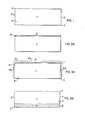
- Figures 1 through 7 show the steps of a preferred embodiment of the method of the present invention.
- a substrate 10 of semiconductor material having top and bottom surfaces 11 and 12, respectively, and having a p-type conductivity is shown in Figure 1.
- a thin layer of phosphorous ions as shown by the heavily stippled area at 20 approximately 1 pm-2 um thick is formed on the top surface 11 by ion implantation.
- Phosphorous ions are donor-type ions and therefore the layer 20 is of n-type conductivity.
- Ion implantation is used in order to control and precisely determine the density of phosphorous atoms in the layer 20 within a narrow range. However, any method by which the density of phosphorous ions can be controlled and precisely determined within a narrow range can be used.
- the ion implantation should be controlled so that the density of the layer 20 is approximately l X l0 18 phosphorous ions/cm 2.
- a layer of oxide 24 is deposited over the top surface 11 and the sides 13 and 14 of the substrate 10 resulting in a structure as shown in Figure 3A. This may be accomplished, of course, by depositing oxide over the entire substrate 10 and then removing it from the surface 12 by a dilute HF etching solution, for example.
- the substrate 10 is heated in a phosphorous diffusion furnace at a temperature of about 1200°C for approximately 33 hours. This simultaneously creates a thick n +- type cathode layer 28 on the bottom surface 12 and causes the layer 20 to extend deeper into the substrate 10.
- the oxide layer 24 prevents the phosphorous in the furnace from diffusing into the layer 20 so as to maintain the precisely determined number of phosphorous ions.
- the density of the layer 20 is lower than the density at the step illustrated by the Figures 2A and 3A.
- the final density of the layer as shown by the lightly stippled area at 23 in Figure 4 is preferred to be approximately 10 17 phosphorous ions/cm 3 .
- Heating the substrate 10 at a temperature of 1200°C for 33 hours will cause the layer 20 to extend approximately 30 total ⁇ m into the substrate 10.
- any time-temperature combination can be used so long as the layer 20 is caused to extend into the substrate 10 so as to lower the final density of the layer 23 to approximately 10 17 phosphorous ions/cm 3 .
- the oxide layer 24 is removed by a dilute HF etching solution and the substrate 10 at the end of this step is shown in Figure 4.
- the impurity concentration of the n-type layer 23 is required to be so low, of course, so as to provide a high lateral resistance in order to create a forward voltage sufficient to forward-bias the subsequently formed anode junction and turn-on the subsequently formed complete thyristor (as shown in Figure 9).
- Another method of forming the n-type layers 23 and 28 of Figure 4 begins with the step of depositing a layer of phosphorous atoms on the bottom surface 12 in order to form the layer 28 as shown in Figure 2B.
- a layer 25 of oxide doped with phosphorous ions as shown by the lightly stippled area at 25, is deposited over the top surface 11 as shown in Figure 3B. Again, this can be done by depositing oxide over the entire substrate 10 and removing it from the sides 13 and 14 and the bottom surface 12 by a dilute HF etching solution.
- the substrate 10 is then heated in a furnace at a temperature of about 1200° for approximately 33 hours.
- the concentration of the phosphorous ions in the oxide layer 25 should be controlled and precisely determined within a small range of concentrations such that the phosphorous ions in the oxide diffuse into the subtrate 10 through the top surface 11 to a depth of about 30 pm.
- the oxide layer 25 is removed by a dilute HF etching solution and the substrate 10 at the end of this step is shown in Figure 4.
- a 20 ⁇ m deep p-type region 30 is diffused into the n-type layer 20 in order to form an anode region having an impurity concentration of about 10 21 acceptor atoms/cm 3 .
- This can be accomplished by any one of several conventional methods depending upon whether or not a shunted anode configuration is desired.
- an oxide mask on the surface 11 can be used where anode shunts are desired and no oxide mask is used where no anode shunts are desired.
- a diffusion of boron through an oxide mask 26 can be used to form the region 30.
- the oxide mask 26 can, as before, be formed by depositing oxide over the entire substrate 10 and removing the oxide, for example, by etching from the sides 1 3 and 14, the bottom surface 12, and from selected portions of the top surface 11 through an etching mask. The oxide mask 26 is then removed leaving a device such as is shown in Figure 5.
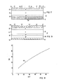
- a 5 ⁇ 10 ⁇ m thick p + -type impurity layer 40 having an impurity concentration from 5 ⁇ 10 17 acceptor atoms/cm 3 to 5 ⁇ 10 18 acceptor atoms/cm 3 is formed in the p-type substrate 10 adjacent to the n +- type layer 28.
- the layer 40 is formed by irradiating the bottom surface 12 for from 20 seconds to 200 seconds with boron ions, for example, from a tandem Van de Graaff generator which can impart to the boron ions a high energy of up to about 36 MeV.
- the boron atoms will penetrate to approximately 50 ⁇ m which will cause an increased impurity concentration in a 5 ⁇ m thick region adjacent to the 50 ⁇ m thick n +- type layer 28.
- This increase in impurity concentration will be accompanied by some damage to the silicon lattice in the p-type substrate 10 caused by the penetrating boron atoms, which lattice damage can be annealed out (repaired) by, for example, heating the substrate 10 in a furnace preferably at a temperature of 600°C-650°C for a period of 1 hour.
- Figure 8 shows a curve 45 plotted on a graph having as an ordinate the energy in units of MeV of the boron ions and having as an abscissa the range or depth of penetration of the boron ions in units of pm. It can be observed that for a penetration of 50 ⁇ m an energy of 36 MeV is required. Other relationships can be determined from the curve 45 in the graph of Figure 8 as required.
- the boron ions penetrate and travel through the n +- type layer 28, they lose energy primarily by electrical interactions with atomic electrons causing no displacing of silicon atoms in the process until the energy of the boron ions reaches a level of about 0.4 MeV. At this energy level, the primary energy loss is due to displacement (physical) collisions with silicon atoms. That is, atoms are displaced from their lattice position. This displacement damage is the type of damage requiring repair by, for example, annealing.
- Each boron ion is provided with an energy within a range E o ⁇ where s is a measure of energy spread from a central energy E n .
- the range of depths to which the ions will penetrate increases as ⁇ increases.
- the theoretical minimum thickness of the p +- type layer 40 is approximately 5 ⁇ m for a beam of boron ions at an energy of 36 MeV.
- the ion beam produced by conventional Van de Graaff accelerators is typically a well-focused one having a diameter on the order of 1 cm.
- the beam can be spread over the surface of a semiconductor wafer such as the substrate 10 by a thin scattering foil or by scanning horizontally and vertically using coils.
- a 60 mils thick cathode electrode 51 is formed by alloying molybdenum to the silicon by an aluminum solder on the bottom surface 12. Aluminum is evaporated on the top surface 11 for forming a 6 ⁇ m thick anode and the completed device is sintered, bevelled, and passivated.
Landscapes
- Thyristors (AREA)
Applications Claiming Priority (2)
| Application Number | Priority Date | Filing Date | Title |
|---|---|---|---|
| US100680 | 1979-12-05 | ||
| US06/100,680 US4278476A (en) | 1979-12-05 | 1979-12-05 | Method of making ion implanted reverse-conducting thyristor |
Publications (3)
| Publication Number | Publication Date |
|---|---|
| EP0030370A2 EP0030370A2 (en) | 1981-06-17 |
| EP0030370A3 EP0030370A3 (en) | 1981-09-16 |
| EP0030370B1 true EP0030370B1 (en) | 1985-04-24 |
Family
ID=22280989
Family Applications (1)
| Application Number | Title | Priority Date | Filing Date |
|---|---|---|---|
| EP80107602A Expired EP0030370B1 (en) | 1979-12-05 | 1980-12-04 | Ion implanted reverse-conducting thyristor |
Country Status (7)
| Country | Link |
|---|---|
| US (1) | US4278476A (ref) |
| EP (1) | EP0030370B1 (ref) |
| JP (1) | JPS5693366A (ref) |
| BR (1) | BR8007898A (ref) |
| CA (1) | CA1144285A (ref) |
| DE (1) | DE3070561D1 (ref) |
| IN (1) | IN152658B (ref) |
Cited By (1)
| Publication number | Priority date | Publication date | Assignee | Title |
|---|---|---|---|---|
| DE4121375A1 (de) * | 1991-06-28 | 1993-01-14 | Asea Brown Boveri | Abschaltbares leistungshalbleiter-bauelement sowie verfahren zu dessen herstellung |
Families Citing this family (11)
| Publication number | Priority date | Publication date | Assignee | Title |
|---|---|---|---|---|
| US4320571A (en) * | 1980-10-14 | 1982-03-23 | International Rectifier Corporation | Stencil mask process for high power, high speed controlled rectifiers |
| EP0074133B1 (de) * | 1981-08-25 | 1987-01-28 | BBC Aktiengesellschaft Brown, Boveri & Cie. | Thyristor |
| JPS5860577A (ja) * | 1981-10-07 | 1983-04-11 | Hitachi Ltd | 半導体装置 |
| US4623910A (en) | 1982-09-24 | 1986-11-18 | Risberg Robert L | Semiconductor device |
| DE3404834A1 (de) * | 1984-02-08 | 1985-08-08 | Hahn-Meitner-Institut für Kernforschung Berlin GmbH, 1000 Berlin | Halbleiter-leistungsbauelement, insbesondere thyristor und gridistor, sowie verfahren zu dessen herstellung |
| JP2579979B2 (ja) * | 1987-02-26 | 1997-02-12 | 株式会社東芝 | 半導体素子の製造方法 |
| JPH0642542B2 (ja) * | 1988-04-08 | 1994-06-01 | 株式会社東芝 | 高耐圧半導体装置の製造方法 |
| US5136344A (en) * | 1988-11-02 | 1992-08-04 | Universal Energy Systems, Inc. | High energy ion implanted silicon on insulator structure |
| US5426059A (en) * | 1994-05-26 | 1995-06-20 | Queyssac; Daniel G. | Method of making vertically stacked bipolar semiconductor structure |
| US6787816B1 (en) * | 2000-09-01 | 2004-09-07 | Rensselaer Polytechnic Institute | Thyristor having one or more doped layers |
| KR100934829B1 (ko) * | 2008-02-15 | 2009-12-31 | 주식회사 하이닉스반도체 | 사이리스터 및 그 제조방법 |
Citations (1)
| Publication number | Priority date | Publication date | Assignee | Title |
|---|---|---|---|---|
| US3622382A (en) * | 1969-05-05 | 1971-11-23 | Ibm | Semiconductor isolation structure and method of producing |
Family Cites Families (13)
| Publication number | Priority date | Publication date | Assignee | Title |
|---|---|---|---|---|
| US3324359A (en) * | 1963-09-30 | 1967-06-06 | Gen Electric | Four layer semiconductor switch with the third layer defining a continuous, uninterrupted internal junction |
| US3428870A (en) * | 1965-07-29 | 1969-02-18 | Gen Electric | Semiconductor devices |
| US3641403A (en) * | 1970-05-25 | 1972-02-08 | Mitsubishi Electric Corp | Thyristor with degenerate semiconductive region |
| US3662382A (en) * | 1970-11-09 | 1972-05-09 | Camera And Instr Corp | Keyboard controlled electrical code-signal generator system |
| US4049478A (en) * | 1971-05-12 | 1977-09-20 | Ibm Corporation | Utilization of an arsenic diffused emitter in the fabrication of a high performance semiconductor device |
| US4009059A (en) * | 1972-01-08 | 1977-02-22 | Mitsubishi Denki Kabushiki Kaisha | Reverse conducting thyristor and process for producing the same |
| FR2274140A1 (fr) * | 1974-06-04 | 1976-01-02 | Alsthom Cgee | Thyristor a conduction inverse |
| CH579827A5 (ref) * | 1974-11-04 | 1976-09-15 | Bbc Brown Boveri & Cie | |
| CH580339A5 (ref) * | 1974-12-23 | 1976-09-30 | Bbc Brown Boveri & Cie | |
| US4038106A (en) * | 1975-04-30 | 1977-07-26 | Rca Corporation | Four-layer trapatt diode and method for making same |
| US4080620A (en) * | 1975-11-17 | 1978-03-21 | Westinghouse Electric Corporation | Reverse switching rectifier and method for making same |
| US4111720A (en) * | 1977-03-31 | 1978-09-05 | International Business Machines Corporation | Method for forming a non-epitaxial bipolar integrated circuit |
| US4168990A (en) * | 1977-04-04 | 1979-09-25 | International Rectifier Corporation | Hot implantation at 1100°-1300° C. for forming non-gaussian impurity profile |
-
1979
- 1979-12-05 US US06/100,680 patent/US4278476A/en not_active Expired - Lifetime
-
1980
- 1980-11-28 IN IN1319/CAL/80A patent/IN152658B/en unknown
- 1980-12-03 BR BR8007898A patent/BR8007898A/pt unknown
- 1980-12-03 CA CA000366042A patent/CA1144285A/en not_active Expired
- 1980-12-04 EP EP80107602A patent/EP0030370B1/en not_active Expired
- 1980-12-04 DE DE8080107602T patent/DE3070561D1/de not_active Expired
- 1980-12-05 JP JP17108480A patent/JPS5693366A/ja active Pending
Patent Citations (1)
| Publication number | Priority date | Publication date | Assignee | Title |
|---|---|---|---|---|
| US3622382A (en) * | 1969-05-05 | 1971-11-23 | Ibm | Semiconductor isolation structure and method of producing |
Cited By (1)
| Publication number | Priority date | Publication date | Assignee | Title |
|---|---|---|---|---|
| DE4121375A1 (de) * | 1991-06-28 | 1993-01-14 | Asea Brown Boveri | Abschaltbares leistungshalbleiter-bauelement sowie verfahren zu dessen herstellung |
Also Published As
| Publication number | Publication date |
|---|---|
| CA1144285A (en) | 1983-04-05 |
| DE3070561D1 (en) | 1985-05-30 |
| BR8007898A (pt) | 1981-06-16 |
| JPS5693366A (en) | 1981-07-28 |
| EP0030370A2 (en) | 1981-06-17 |
| EP0030370A3 (en) | 1981-09-16 |
| US4278476A (en) | 1981-07-14 |
| IN152658B (ref) | 1984-03-03 |
Similar Documents
| Publication | Publication Date | Title |
|---|---|---|
| US3897274A (en) | Method of fabricating dielectrically isolated semiconductor structures | |
| US6168981B1 (en) | Method and apparatus for the localized reduction of the lifetime of charge carriers, particularly in integrated electronic devices | |
| CA1081863A (en) | Reducing the switching time of semiconductor devices by nuclear irradiation | |
| US5017508A (en) | Method of annealing fully-fabricated, radiation damaged semiconductor devices | |
| EP0030370B1 (en) | Ion implanted reverse-conducting thyristor | |
| US6603153B2 (en) | Fast recovery diode and method for its manufacture | |
| CA1162326A (en) | Forming impurity regions in semiconductor bodies by high energy ion irradiation, and semiconductor devices made thereby | |
| JP3968129B2 (ja) | 高速パワーダイオード | |
| US4004950A (en) | Method for improving the doping of a semiconductor material | |
| US4151011A (en) | Process of producing semiconductor thermally sensitive switching element by selective implantation of inert ions in thyristor structure | |
| US3950187A (en) | Method and apparatus involving pulsed electron beam processing of semiconductor devices | |
| US4240844A (en) | Reducing the switching time of semiconductor devices by neutron irradiation | |
| US6762080B2 (en) | Method of manufacturing a semiconductor device having a cathode and an anode from a wafer | |
| JP2003224281A (ja) | 半導体装置およびその製造方法 | |
| EP1246255B1 (en) | Insulated gate bipolar transistor | |
| US7534666B2 (en) | High voltage non punch through IGBT for switch mode power supplies | |
| EP0125138B1 (en) | Self protected thyristor and method of making | |
| US4135292A (en) | Integrated circuit contact and method for fabricating the same | |
| US4534806A (en) | Method for manufacturing vertical PNP transistor with shallow emitter | |
| US4075037A (en) | Tailoring of recovery charge in power diodes and thyristors by irradiation | |
| EP1298717A1 (en) | Method for manufacturing a semiconductor device having a pn junction area | |
| US3918996A (en) | Formation of integrated circuits using proton enhanced diffusion | |
| KR100299912B1 (ko) | 절연 게이트 바이폴라 트랜지스터의 제조 방법 | |
| US20250318225A1 (en) | Semiconductor device and method for manufacturing semiconductor device | |
| US3822153A (en) | Method for fabricating a double drift diode |
Legal Events
| Date | Code | Title | Description |
|---|---|---|---|
| PUAI | Public reference made under article 153(3) epc to a published international application that has entered the european phase |
Free format text: ORIGINAL CODE: 0009012 |
|
| AK | Designated contracting states |
Kind code of ref document: A2 Designated state(s): BE DE FR GB |
|
| PUAL | Search report despatched |
Free format text: ORIGINAL CODE: 0009013 |
|
| AK | Designated contracting states |
Kind code of ref document: A3 Designated state(s): BE DE FR GB |
|
| 17P | Request for examination filed |
Effective date: 19820212 |
|
| GRAA | (expected) grant |
Free format text: ORIGINAL CODE: 0009210 |
|
| AK | Designated contracting states |
Kind code of ref document: B1 Designated state(s): BE DE FR GB |
|
| REF | Corresponds to: |
Ref document number: 3070561 Country of ref document: DE Date of ref document: 19850530 |
|
| ET | Fr: translation filed | ||
| PLBE | No opposition filed within time limit |
Free format text: ORIGINAL CODE: 0009261 |
|
| STAA | Information on the status of an ep patent application or granted ep patent |
Free format text: STATUS: NO OPPOSITION FILED WITHIN TIME LIMIT |
|
| 26N | No opposition filed | ||
| PG25 | Lapsed in a contracting state [announced via postgrant information from national office to epo] |
Ref country code: BE Effective date: 19881231 |
|
| BERE | Be: lapsed |
Owner name: WESTINGHOUSE ELECTRIC CORP. Effective date: 19881231 |
|
| PGFP | Annual fee paid to national office [announced via postgrant information from national office to epo] |
Ref country code: FR Payment date: 19910917 Year of fee payment: 12 |
|
| PGFP | Annual fee paid to national office [announced via postgrant information from national office to epo] |
Ref country code: GB Payment date: 19910924 Year of fee payment: 12 |
|
| PGFP | Annual fee paid to national office [announced via postgrant information from national office to epo] |
Ref country code: DE Payment date: 19911231 Year of fee payment: 12 |
|
| PG25 | Lapsed in a contracting state [announced via postgrant information from national office to epo] |
Ref country code: GB Effective date: 19921204 |
|
| GBPC | Gb: european patent ceased through non-payment of renewal fee |
Effective date: 19921204 |
|
| PG25 | Lapsed in a contracting state [announced via postgrant information from national office to epo] |
Ref country code: FR Effective date: 19930831 |
|
| PG25 | Lapsed in a contracting state [announced via postgrant information from national office to epo] |
Ref country code: DE Effective date: 19930901 |
|
| REG | Reference to a national code |
Ref country code: FR Ref legal event code: ST |