EP0027072B1 - Procédé de couplage entre une fibre optique et une diode opto-électronique, et tête d'émission ou de réception réalisée par ce procédé - Google Patents
Procédé de couplage entre une fibre optique et une diode opto-électronique, et tête d'émission ou de réception réalisée par ce procédé Download PDFInfo
- Publication number
- EP0027072B1 EP0027072B1 EP80401353A EP80401353A EP0027072B1 EP 0027072 B1 EP0027072 B1 EP 0027072B1 EP 80401353 A EP80401353 A EP 80401353A EP 80401353 A EP80401353 A EP 80401353A EP 0027072 B1 EP0027072 B1 EP 0027072B1
- Authority
- EP
- European Patent Office
- Prior art keywords
- cavity
- opto
- accordance
- diode
- chemical attack
- Prior art date
- Legal status (The legal status is an assumption and is not a legal conclusion. Google has not performed a legal analysis and makes no representation as to the accuracy of the status listed.)
- Expired
Links
Images

Classifications
-
- H—ELECTRICITY
- H10—SEMICONDUCTOR DEVICES; ELECTRIC SOLID-STATE DEVICES NOT OTHERWISE PROVIDED FOR
- H10F—INORGANIC SEMICONDUCTOR DEVICES SENSITIVE TO INFRARED RADIATION, LIGHT, ELECTROMAGNETIC RADIATION OF SHORTER WAVELENGTH OR CORPUSCULAR RADIATION
- H10F77/00—Constructional details of devices covered by this subclass
- H10F77/10—Semiconductor bodies
- H10F77/14—Shape of semiconductor bodies; Shapes, relative sizes or dispositions of semiconductor regions within semiconductor bodies
- H10F77/147—Shapes of bodies
-
- G—PHYSICS
- G02—OPTICS
- G02B—OPTICAL ELEMENTS, SYSTEMS OR APPARATUS
- G02B6/00—Light guides; Structural details of arrangements comprising light guides and other optical elements, e.g. couplings
- G02B6/24—Coupling light guides
- G02B6/42—Coupling light guides with opto-electronic elements
- G02B6/4201—Packages, e.g. shape, construction, internal or external details
- G02B6/4202—Packages, e.g. shape, construction, internal or external details for coupling an active element with fibres without intermediate optical elements, e.g. fibres with plane ends, fibres with shaped ends, bundles
-
- G—PHYSICS
- G02—OPTICS
- G02B—OPTICAL ELEMENTS, SYSTEMS OR APPARATUS
- G02B6/00—Light guides; Structural details of arrangements comprising light guides and other optical elements, e.g. couplings
- G02B6/24—Coupling light guides
- G02B6/42—Coupling light guides with opto-electronic elements
- G02B6/4201—Packages, e.g. shape, construction, internal or external details
- G02B6/4204—Packages, e.g. shape, construction, internal or external details the coupling comprising intermediate optical elements, e.g. lenses, holograms
- G02B6/421—Packages, e.g. shape, construction, internal or external details the coupling comprising intermediate optical elements, e.g. lenses, holograms the intermediate optical component consisting of a short length of fibre, e.g. fibre stub
-
- G—PHYSICS
- G02—OPTICS
- G02B—OPTICAL ELEMENTS, SYSTEMS OR APPARATUS
- G02B6/00—Light guides; Structural details of arrangements comprising light guides and other optical elements, e.g. couplings
- G02B6/24—Coupling light guides
- G02B6/42—Coupling light guides with opto-electronic elements
- G02B6/4201—Packages, e.g. shape, construction, internal or external details
- G02B6/4248—Feed-through connections for the hermetical passage of fibres through a package wall
-
- H—ELECTRICITY
- H10—SEMICONDUCTOR DEVICES; ELECTRIC SOLID-STATE DEVICES NOT OTHERWISE PROVIDED FOR
- H10W—GENERIC PACKAGES, INTERCONNECTIONS, CONNECTORS OR OTHER CONSTRUCTIONAL DETAILS OF DEVICES COVERED BY CLASS H10
- H10W72/00—Interconnections or connectors in packages
- H10W72/851—Dispositions of multiple connectors or interconnections
-
- H—ELECTRICITY
- H10—SEMICONDUCTOR DEVICES; ELECTRIC SOLID-STATE DEVICES NOT OTHERWISE PROVIDED FOR
- H10W—GENERIC PACKAGES, INTERCONNECTIONS, CONNECTORS OR OTHER CONSTRUCTIONAL DETAILS OF DEVICES COVERED BY CLASS H10
- H10W72/00—Interconnections or connectors in packages
- H10W72/50—Bond wires
- H10W72/531—Shapes of wire connectors
- H10W72/536—Shapes of wire connectors the connected ends being ball-shaped
-
- Y—GENERAL TAGGING OF NEW TECHNOLOGICAL DEVELOPMENTS; GENERAL TAGGING OF CROSS-SECTIONAL TECHNOLOGIES SPANNING OVER SEVERAL SECTIONS OF THE IPC; TECHNICAL SUBJECTS COVERED BY FORMER USPC CROSS-REFERENCE ART COLLECTIONS [XRACs] AND DIGESTS
- Y02—TECHNOLOGIES OR APPLICATIONS FOR MITIGATION OR ADAPTATION AGAINST CLIMATE CHANGE
- Y02E—REDUCTION OF GREENHOUSE GAS [GHG] EMISSIONS, RELATED TO ENERGY GENERATION, TRANSMISSION OR DISTRIBUTION
- Y02E10/00—Energy generation through renewable energy sources
- Y02E10/50—Photovoltaic [PV] energy
Definitions
- the invention relates to a method of coupling between an optical fiber and a photo-receiving or photo-emitting diode as well as an opto-electronic head produced using such a method.
- an opto-electronic head constitutes a transition point between an optical fiber and a component, generally a semiconductor, constituting the optical terminal, on reception or on transmission, of a telecommunications link.
- the optical fiber In an opto-electronic head, the optical fiber has a generally very small diameter, sometimes up to 50 microns; if the component is a receiving photodiode, the dimensions of the photodetector surface are also very small.
- the optical fiber In a conventional type head, the optical fiber is mounted in a fiber holder from which it emerges from the diode side, the photodiode being mounted on a base which adapts to the fiber holder. The respective positioning of the fiber and the diode must therefore be extremely precise. It follows that the manufacture of such heads is in the field of precision mechanics and that their production cost is high.
- the invention makes it possible to simplify the problem of relative positioning between the fiber and the component (photodiode for example) by providing a new coupling method.
- the photodiode present on a face intended to be coupled to the optical fiber, at least one cavity in the form of a cuvette, possibly hemispherical, in which the end of the optical fiber will be housed.
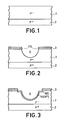
- FIG. 1 there is shown in partial section a semiconductor wafer comprising for example a substrate 1 doped P-, and a layer 2 doped P + .
- the thickness of the substrate is much greater than the diameter of the optical fiber intended to be coupled to the semiconductor structure after the production, in this structure, of a diode, for example photodetector.
- the realization of such a structure, by conventional means, constitutes step (a) of the process.
- FIG. 2 shows the same pellet after chemical attack carried out on the face of the substrate 1 opposite to the layer 2. This face had previously been covered with a layer of silica 3, deposited for example by sputtering. A window 30 had also been arranged in the layer 3 by conventional means such as a deposit of resin then removed using a solvent. These preliminary steps of step (b) of the method according to the invention are not shown.
- step (b) the chemical attack is carried out for example using a rapid agent, for example a mixture of hydrofluoric acid and nitric acid in the case of a silicon substrate.
- a rapid agent for example a mixture of hydrofluoric acid and nitric acid in the case of a silicon substrate.
- step (c) of the method doping is carried out, by an N-type impurity, of the semiconductor wafer previously protected on the faces other than that of layer 3. Doping is continued until obtaining a high rate (N + ) in a layer 19 as is conventional in photodetector diodes of the type of the example considered, and this in order to improve the quantity of the electrical connection contact of the diode.
- the layer 3 has been previously eliminated on the edge of the cavity 4 so as to provide a doped zone 101. This operation can be done by selective chemical attack after protection of the rest of the layer 3.
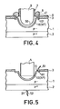
- step (d) of the method the end 50 of an optical fiber 5 is introduced into the cavity 4 (FIG. 4).
- the part 50 has been rounded beforehand by one of the now conventional methods, such as a fusion of the end of the optical fiber or the addition of glass in fusion.
- the diode has been metallized, after chemical attack on the layer 3 to expose the edge 41 of the cavity 4 beforehand.
- the metal deposition 6 is carried out while sparing on at least part of the edge 41.
- FIG. 4 also partially represents an optical fiber 5, the end of which is covered with a metallization 7.
- the metallizations 6 and 7 can then be electrically connected using an annular weld bead 8.
- the polarization of the diode can then be carried out by connecting to the metallized part of the optical fiber, which can be advantageous for certain opto-electronic head models.
- connections 51 and 52 are respectively welded to contacts 11 and 21 arranged on the zone 101 of the N + layer and on the P + layer,
- a slow-attack chemical agent is used to create the cavity 4. Under these conditions, a flat bottom cavity is obtained.
- the coupling of the diode with an optical fiber terminated in a cross section, as in the first variant, is then better than in the case of a cavity in a spherical cap.
- the connections are made in the same way as in the first variant.
- the method according to the invention makes it possible to produce a simpler opto-electronic head and of reduced volume than conventional heads.
- connection 51 (N + layer) is connected to the metallization 7 of the optical fiber 5 by the addition of a metallization 73 on the face of the base 712 of the fiber holder, diode side.
- a weld bead 74 connects the metallizations 7 and 73.
- the end piece 711 of the fiber holder has a central perforation 75 wide enough to allow the immobilization of the optical fiber by glue or resin. It should be noted that, for the purpose of clarification, the drawing in FIG. 7 is not to scale.
- the diameter of the optical fiber being of the order of a tenth of a millimeter
- the end piece 711 and the base 712 have for example respective diameters of 3 and 20 mm.
- the contact with the P + layer it is connected by a connection 52 which passes through the coating 72.
- the invention is applicable to light-emitting diodes as to photodetector diodes installed in terminal equipment for short and medium distance optical links.
Landscapes
- Physics & Mathematics (AREA)
- General Physics & Mathematics (AREA)
- Optics & Photonics (AREA)
- Optical Couplings Of Light Guides (AREA)
- Light Receiving Elements (AREA)
Description
- L'invention concerne un procédé de couplage entre une fibre optique et une diode photo- réceptrice ou photo-émettrice ainsi qu'une tête opto-électronique réalisée en utilisant un tel procédé.
- On sait qu'une tête opto-électronique constitue un point de transition entre une fibre optique et un composant, généralement à semiconducteur, constituant le terminal optique, à la réception ou à l'émission, d'une liaison de télécommunications.
- Dans une tête opto-électronique, la fibre optique présente un diamètre généralement très petit, parfois jusqu'à 50 microns; si le composant est une photodiode de réception, les dimensions de la surface photodétectrice sont également très petites. Dans une tête de type classique, la fibre optique est montée dans un porte-fibre dont elle émerge du côté diode, la photodiode étant montée sur une embase qui s'adapte au porte-fibre. Les positionnement respectifs de la fibre et de la diode doivent, en conséquence, être extrêmement précis. Il en résulte que la fabrication de telles têtes est du domaine de la mécanique de précision et que leur coût de production est élevé.
- L'invention permet de simplifier le problème de positionnement relatif entre la fibre et le composant (photodiode par exemple) en fournissant un nouveau procédé de couplage. A cet effet la photodiode présente sur une face destinée à être couplée à la fibre optique, au moins une cavité en forme de cuvette, éventuellement hémisphérique, dans laquelle on logera l'extrémité de la fibre optique.
- Une telle cavité, présentant sur ses parois une jonction semiconductrice, est réalisable par attaque chimique suivie d'une diffusion d'impuretés dopantes dans une pastille semiconductrice, selon des conditions précisées par le brevet français de la demanderesse publié sous le N° 1.536.424, relatif aux "Perfectionnements aux diodes semiconductrices de structure planar pour hautes fréquences".
- La mise en place de l'extrémité de la fibre optique devient alors beaucoup plus facile qu'en l'absence d'une telle cavité. De plus on peut alors éliminer l'ambase classique de la tête opto-électronique et la remplacer par une simple protection en matière plastique traversée par les connexions de raccordement de l'anode et de la cathode de la photodiode.
- Une telle cavité est décrite, aussi, dans le facicule de brevet US-A-4 010483 qui décrit un procédé de couplage comportant les étapes suivantes:
- (a) réalisation d'une structure semiconductrice destinée à constituer une diode opto-électronique par la formation ultérieure d'une couche semiconductrice dopée de façon à constituer avec le reste de la structure une jonction redresseuse;
- (b) formation d'une cavité par attaque chimique de la structure destinée à être couplée à la fibre optique et à être le siège de la jonction redresseuse, l'attaque chimique étant localisée dans une zone superficielle délimitée par une couche de matériau résistant à l'attaque chimique;
- (c) formation de la jonction redresseuse par dopage du matériau semiconducteur constituant la paroi interne de la cavité;
- (d) réalisation d'une tête opto-électronique par mise en place de l'extrémité d'une fibre optique dans la cavité de la structure.
- En comparaison de cet état de la technique, le procédé de couplage selon l'invention est principalement caractérisé en ce que:
- - la structure semiconductrice de l'étape (a) est formée d'une ou de plusieurs parties présentant toutes le même type de conductivité;
- - le matériau de dopage sélectionné au cours de l'étape (c) est de type de conductivité contraire, de façon que la zone superficielle dopée de la cavité constitue, avec le reste de la structure, la jonction redresseuse.
- L'invention a donc pour objet un procédé de couplage entre une fibre optique et une diode opto-électronique, comportant les étapes suivantes:
- (a) réalisation d'une structure semiconductrice destinée à constituer une diode opto-électronique par la formation ultérieure d'une couche semiconductrice dopée de façon à constituer avec le reste de la structure une jonction redresseuse;
- (b) formation d'une cavité par attaque chimique de la structure destinée à être couplée à la fibre optique et à être le siège de la jonction redresseuse, l'attaque chimique étant localisée dans une zone superficielle délimitée par une couche de matériau résistant à l'attaque chimique;
- (c) formation de la jonction redresseuse par dopage du matériau semiconducteur constituant la paroi interne de la cavité;
- (d) réalisation d'une tête opto-électroniqùe par mise en place de l'extrémité d'une fibre optique dans la cavité de la structure;
- L'invention sera mieux comprise, et d'autres caractéristiques apparaitront, au moyen de la description qui suit, et des dessins qui l'accompagnent, parmi lesquels:
- - les figures 1 à 4 représentent en coupe partielle différentes étapes de réalisation du procédé selon l'invention;
- - les figures 5 et 6 représentent des variantes du procédé;
- -la figure 7 représente une tête opto-électronique réalisée en utilisant le procédé selon l'invention.
- Figure 1, on a représenté en coupe partielle une pastille semiconductrice comportant par exemple un substrat 1 dopé P-, et une couche 2 dopée P+. L'épaisseur de substrat est largement supérieure au diamètre de la fibre optique destinée à être couplée à la structure semiconductrice après la réalisation, dans cette structure, d'une diode, par exemple photodétectrice. La réalisation d'une telle structure, par des moyens classiques, constitue l'étape (a) du procédé.
- Figure 2, on a représenté la même pastille après attaque chimique effectuée sur la face du substrat 1 opposée à la couche 2. Cette face avait été préalablement recouverte par une couche de silice 3, déposée par exemple par pulvérisation cathodique. Une fenêtre 30 avait également été aménagée dans la couche 3 par un moyen classique tel qu'un dépôt de résine éliminé ensuite à l'aide d'un solvant. Ces étapes préliminaires de l'étape (b), du procédé selon l'invention ne sont pas représentées.
- Au cours de l'étape (b) proprement dit, l'attaque chimique est effectuée par exemple en utilisant un agent rapide, par exemple un mélange d'acide fluorhydrique et d'acide nitrique dans le cas d'un substrat en silicium. On obtient alors une cavité 4 en forme de calotte sphérique.
- Au cours de l'étape (c) du procédé, on effectue le dopage, par une impureté de type N, de la pastille semiconductrice préalablement protégée sur les faces autres que celle de la couche 3. Le dopage est poursuivi jusqu'à l'obtention d'un taux élevé (N+) dans une couche 19 comme il est classique dans les diodes photodétectrices du type de l'exemple considéré, et cela pour améliorer la quantité du contact de raccordement électrique de la diode. La couche 3 a été préalablement éliminée sur le bord de la cavité 4 de façon à aménager une zone dopée 101. Cette opération peut se faire par attaque chimique sélective après protection du reste de la couche 3.
- A l'étape (d) du procédé, on introduit l'extrémité 50 d'une fibre optique 5 dans la cavité 4 (figure 4). A titre d'exemple, pour améliorer le couplage optique entre fibre et diode, on a préalablement arrondi la partie 50 par un des procédés maintenant classiques, telle qu'une fusion de l'extrémité de la fibre optique ou l'apport de verre en fusion.
- Dans la réalisation représenté à titre d'exemple, figure 4, la diode a été métallisée, après attaque chimique de la couche 3 pour mettre préalablement à nu le bord 41 de la cavité 4. Le dépôt métallique 6 est effectué en ménageant une épargne sur une partie au moins du bord 41. La figure 4 représente en outre partiellement une fibre optique 5 dont l'extrémité est recouverte d'une métallisation 7. Les métallisations 6 et 7 peuvent ensuite être raccordées électriquement en utilisant un cordon de soudure annulaire 8. La polarisation de la diode peut alors être effectuée en se raccordant à la partie métallisée de la fibre optique, ce qui peut être avantageux pour certains modèles de tête opto-électronique.
- Dans une première variante simplifiée de l'invention, représentée figure 5, on se contente de mettre en place une fibre optique 5 sans lui faire subir aucun traitement ayant pour but d'arrondir l'extrémité à coupler à la diode ou à métalliser une partie de la fibre. Des connexions 51 et 52 sont soudées respectivement à des contacts 11 et 21 aménagés sur la zone 101 de la couche N+ et sur la couche P+,
- Dans une deuxième variante simplifiée, représentée figure 6, on utilise, pour créer la cavité 4, un agent chimique d'attaque lente. Dans ces conditions, on obtient une cavité à fond plat. Le couplage de la diode avec une fibre optique terminée par une section droite, comme dans la première variante, est alors meilleur que dans le cas d'une cavité en calotte sphérique. Les connexions sont réalisées de la même façon que dans la première variante.
- Le procédé selon l'invention permet de réaliser une tête opto-électronique plus simple et de volume plus réduit que les têtes classiques.
- En prenant comme point de départ la réalisation représentée figure 4, il suffit, pour obtenir une telle tête, d'adjoindre au dispositif de départ un porte-fibre 71 et un enrobage 72 par exemple en résine synthétique. La connexion 51 (couche N+) est reliée à la métallisation 7 de la fibre optique 5 grâce à l'adjonction d'une métallisation 73 sur la face de l'embase 712 du porte-fibre, côté diode. Un cordon de soudure 74 relie les métallisations 7 et 73. L'embout 711 du porte-fibre comporte une perforation centrale 75 assez large pour permettre l'immobilisation de la fibre optique par la colle ou de la résine. Il est à noter que, dans un but de clarification, le dessin de la figure 7 n'est pas à l'échelle. En effet, le diamètre de la fibre optique étant de l'ordre du dixième de millimètre, l'embout 711 et l'embase 712 ont par exemple des diamètres respectifs de 3 et de 20 mm. Quant au contact avec la couche P+, il est raccordé par une connexion 52 qui traverse l'enrobage 72.
- L'invention est applicable aux diodes électroluminescentes comme aux diodes photodétectrices mises en place dans les équipements terminaux de liaisons optiques à petite et à moyenne distances.
caractérisé en ce que la structure semiconductrice de l'étape (a) est formée d'une ou de plusieurs parties présentant toutes le même type de conductivité, le matériau de dopage sélectionné au cours de l'étape (c) étant de type conductivité contraire, de façon que la zone superficielle dopée de la cavité constitue, avec le reste de la structure, la jonction redresseuse.
Claims (10)
Applications Claiming Priority (2)
| Application Number | Priority Date | Filing Date | Title |
|---|---|---|---|
| FR7924891A FR2466866A1 (fr) | 1979-10-05 | 1979-10-05 | Procede de couplage entre une fibre optique et une diode opto-electronique, et tete d'emission ou de reception realisee par ce procede |
| FR7924891 | 1979-10-05 |
Publications (2)
| Publication Number | Publication Date |
|---|---|
| EP0027072A1 EP0027072A1 (fr) | 1981-04-15 |
| EP0027072B1 true EP0027072B1 (fr) | 1983-05-18 |
Family
ID=9230384
Family Applications (1)
| Application Number | Title | Priority Date | Filing Date |
|---|---|---|---|
| EP80401353A Expired EP0027072B1 (fr) | 1979-10-05 | 1980-09-23 | Procédé de couplage entre une fibre optique et une diode opto-électronique, et tête d'émission ou de réception réalisée par ce procédé |
Country Status (4)
| Country | Link |
|---|---|
| US (1) | US4326771A (fr) |
| EP (1) | EP0027072B1 (fr) |
| DE (1) | DE3063348D1 (fr) |
| FR (1) | FR2466866A1 (fr) |
Cited By (1)
| Publication number | Priority date | Publication date | Assignee | Title |
|---|---|---|---|---|
| DE102006058622A1 (de) * | 2006-12-11 | 2008-06-19 | Schleifring Und Apparatebau Gmbh | Empfangseinheit für einen optischen Drehübertrager |
Families Citing this family (33)
| Publication number | Priority date | Publication date | Assignee | Title |
|---|---|---|---|---|
| FR2458825A1 (fr) * | 1979-06-08 | 1981-01-02 | Thomson Csf | Procede de montage d'une fibre optique dans un embout, embout ainsi monte, et dispositif de connexion de fibres optiques utilisant cet embout |
| US4653847A (en) * | 1981-02-23 | 1987-03-31 | Motorola, Inc. | Fiber optics semiconductor package |
| US4461537A (en) * | 1981-12-24 | 1984-07-24 | Molex Incorporated | Fiber optic connector assembly |
| US4784454A (en) * | 1982-08-02 | 1988-11-15 | Andrew Corporation | Optical fiber and laser interface device |
| CA1267468C (fr) * | 1983-11-21 | 1990-04-03 | Montage d'optique | |
| US4647147A (en) * | 1984-01-20 | 1987-03-03 | Hughes Aircraft Company | Fiber optic to integrated optical chip coupler |
| CA1255382A (fr) * | 1984-08-10 | 1989-06-06 | Masao Kawachi | Circuit integre optique hybride a guides d'alignement |
| US4616899A (en) * | 1984-08-31 | 1986-10-14 | Gte Laboratories Incorporated | Methods of and apparatus for coupling an optoelectronic component to an optical fiber |
| US4675624A (en) * | 1985-03-29 | 1987-06-23 | Rca Corporation | Electrical phase shifter controlled by light |
| US4744623A (en) * | 1985-10-16 | 1988-05-17 | The Trustees Of Columbia University In The City Of New York | Integrated fiber optic coupler for VHSIC/VLSI interconnects |
| CA1271550C (fr) * | 1985-12-24 | 1990-07-10 | Dispositif luminescent a semiconducteur, eclairant a la verticale | |
| US4779946A (en) * | 1986-02-14 | 1988-10-25 | American Telephone And Telegraph Company, At&T Bell Laboratories | Microminiature optical assembly |
| US4751513A (en) * | 1986-05-02 | 1988-06-14 | Rca Corporation | Light controlled antennas |
| US4812002A (en) * | 1986-10-24 | 1989-03-14 | Hitachi, Ltd. | Optical coupling device and method of making the same |
| US4892374A (en) * | 1988-03-03 | 1990-01-09 | American Telephone And Telegraph Company, At&T Bell Laboratories | Article comprising an opto-electronic device and an optical waveguide coupled thereto, and method of making the article |
| US4995695A (en) * | 1989-08-17 | 1991-02-26 | At&T Bell Laboratories | Optical assembly comprising optical fiber coupling means |
| US4977107A (en) * | 1989-08-23 | 1990-12-11 | Motorola Inc. | Method for manufacturing semiconductor rectifier |
| DE4002490A1 (de) * | 1989-08-31 | 1991-08-01 | Bodenseewerk Geraetetech | Verfahren zum anbringen von elektrooptischen bauteilen an integriert-optischen wellenleitern |
| US5051789A (en) * | 1990-10-11 | 1991-09-24 | The United States Of America As Represented By The United States Department Of Energy | Device having two optical ports for switching applications |
| US5221641A (en) * | 1991-06-21 | 1993-06-22 | Rohm Co., Ltd. | Process for making light emitting diodes |
| US5308656A (en) * | 1991-07-16 | 1994-05-03 | Adc Telecommunications, Inc. | Electroformed mask and use therefore |
| JP3093049B2 (ja) * | 1992-09-22 | 2000-10-03 | ローム株式会社 | 光分岐結合器 |
| JPH06237016A (ja) * | 1993-02-09 | 1994-08-23 | Matsushita Electric Ind Co Ltd | 光ファイバモジュールおよびその製造方法 |
| US5546413A (en) * | 1994-09-01 | 1996-08-13 | Motorola | Integrated light emitting device |
| US5575929A (en) * | 1995-06-05 | 1996-11-19 | The Regents Of The University Of California | Method for making circular tubular channels with two silicon wafers |
| JP3166564B2 (ja) * | 1995-06-27 | 2001-05-14 | 松下電器産業株式会社 | 半導体レーザ実装体およびその製造方法 |
| FR2758888B1 (fr) * | 1997-01-27 | 1999-04-23 | Thomson Csf | Procede de modelisation fine du fouillis de sol recu par un radar |
| US6213651B1 (en) | 1999-05-26 | 2001-04-10 | E20 Communications, Inc. | Method and apparatus for vertical board construction of fiber optic transmitters, receivers and transceivers |
| US6901221B1 (en) | 1999-05-27 | 2005-05-31 | Jds Uniphase Corporation | Method and apparatus for improved optical elements for vertical PCB fiber optic modules |
| KR100420951B1 (ko) * | 2002-04-17 | 2004-03-02 | 한국전자통신연구원 | 분극 광섬유, 분극 광섬유를 제조하는 방법 및 분산 보상기 |
| US6913399B2 (en) * | 2003-07-23 | 2005-07-05 | Intel Corporation | Metallized optical fibers and ferrules for optical fibers for direct attachment to photodiodes |
| WO2009144645A1 (fr) | 2008-05-27 | 2009-12-03 | Nxp B.V. | Dispositif de photodétection et son procédé de fabrication |
| JP5452781B1 (ja) * | 2012-06-28 | 2014-03-26 | オリンパスメディカルシステムズ株式会社 | 走査型内視鏡および走査型内視鏡の製造方法 |
Family Cites Families (4)
| Publication number | Priority date | Publication date | Assignee | Title |
|---|---|---|---|---|
| US4010483A (en) * | 1974-08-08 | 1977-03-01 | International Telephone And Telegraph Corporation | Current confining light emitting diode |
| CA1058732A (fr) * | 1976-06-11 | 1979-07-17 | Northern Telecom Limited | Diodes electroluminescentes a luminosite accrue |
| FR2387517A1 (fr) * | 1977-04-13 | 1978-11-10 | Thomson Csf | Systeme d'encapsulation etanche d'un dispositif optoelectronique emetteur ou recepteur a transmission par fibre optique |
| US4227975A (en) * | 1979-01-29 | 1980-10-14 | Bell Telephone Laboratories, Incorporated | Selective plasma etching of dielectric masks in the presence of native oxides of group III-V compound semiconductors |
-
1979
- 1979-10-05 FR FR7924891A patent/FR2466866A1/fr active Granted
-
1980
- 1980-09-23 EP EP80401353A patent/EP0027072B1/fr not_active Expired
- 1980-09-23 DE DE8080401353T patent/DE3063348D1/de not_active Expired
- 1980-10-02 US US06/193,294 patent/US4326771A/en not_active Expired - Lifetime
Cited By (1)
| Publication number | Priority date | Publication date | Assignee | Title |
|---|---|---|---|---|
| DE102006058622A1 (de) * | 2006-12-11 | 2008-06-19 | Schleifring Und Apparatebau Gmbh | Empfangseinheit für einen optischen Drehübertrager |
Also Published As
| Publication number | Publication date |
|---|---|
| EP0027072A1 (fr) | 1981-04-15 |
| DE3063348D1 (en) | 1983-07-07 |
| FR2466866B1 (fr) | 1983-03-18 |
| FR2466866A1 (fr) | 1981-04-10 |
| US4326771A (en) | 1982-04-27 |
Similar Documents
| Publication | Publication Date | Title |
|---|---|---|
| EP0027072A1 (fr) | Procédé de couplage entre une fibre optique et une diode opto-électronique, et tête d'émission ou de réception réalisée par ce procédé | |
| EP3610309B1 (fr) | Puce photonique à structure de collimation intégrée | |
| US4730198A (en) | Aligning arrays of optoelectronic devices to arrays of optical fibers | |
| FR2554606A1 (fr) | Dispositif optique de concentration du rayonnement lumineux emis par une diode electroluminescente, et diode electroluminescente comportant un tel dispositif | |
| US7968429B2 (en) | Method of manufacturing a semiconductor photodetector device by removing the semiconductor substrate on one surface after forming the light-transmitting layer on the opposing surface | |
| EP0860913A2 (fr) | Laser à l'émission de surface à cavité verticale à grande longueurs et méthode de fabrication | |
| US6122109A (en) | Non-planar micro-optical structures | |
| US4745451A (en) | Photodetector array and a method of making same | |
| FR3052915A1 (fr) | Procede de fabrication d'une diode electroluminescente au nitrure de gallium | |
| FR2760101A1 (fr) | Procede d'assemblage d'un dispositif opto-hybride | |
| EP2884547B1 (fr) | Procédé de fabrication d'un photo-détecteur. | |
| EP0817337A1 (fr) | Procédé de fabrication d'un laser à émission par la surface | |
| EP4184594B1 (fr) | Photodiode germanium a courant d obscurite reduit comportant une portion intermediaire peripherique a base de sige/ge | |
| EP3130010B1 (fr) | Dispositif optoelectronique a diodes electroluminescentes et a diagramme d'emission ameliore | |
| FR2538616A1 (fr) | Procede de fabrication collective de diodes hyperfrequence avec encapsulation incorporee et diodes ainsi obtenues | |
| JPS58158620A (ja) | 光通信装置およびこれに用いる光フアイバならびに光フアイバの加工方法 | |
| EP0025728A1 (fr) | Dispositif de couplage entre une source lumineuse à rayonnement divergent, et une fibre optique, et procédé de réalisation d'un tel dispositif | |
| US6716659B2 (en) | Method and apparatus for shaping semiconductor surfaces | |
| CN115588728A (zh) | 利于激光焊接的发光二极管及其制备方法 | |
| WO1990006608A1 (fr) | Procede de realisation de lasers semi-conducteurs et lasers obtenus par le procede | |
| JP2002151732A (ja) | 半導体光検出器の作製方法 | |
| FR2484710A1 (fr) | Diode electroluminescente et son procede de fabrication | |
| EP1189087A2 (fr) | Récepteur photonique monolithique comprenant un support de fibre autoaligné adapté pour assemblage du type flip chip | |
| FR2613381A1 (fr) | Procede d'attaque d'une surface d'une piece en phosphure d'indium | |
| FR2486104A1 (fr) | Procede d'obtention de creusures a contour circulaire dans les monocristaux de composes intermetalliques cristallisant dans le systeme cubique a faces centrees et dispositif comportant de telles creusures |
Legal Events
| Date | Code | Title | Description |
|---|---|---|---|
| PUAI | Public reference made under article 153(3) epc to a published international application that has entered the european phase |
Free format text: ORIGINAL CODE: 0009012 |
|
| AK | Designated contracting states |
Designated state(s): DE GB IT NL |
|
| 17P | Request for examination filed |
Effective date: 19810502 |
|
| ITF | It: translation for a ep patent filed | ||
| GRAA | (expected) grant |
Free format text: ORIGINAL CODE: 0009210 |
|
| AK | Designated contracting states |
Designated state(s): DE GB IT NL |
|
| REF | Corresponds to: |
Ref document number: 3063348 Country of ref document: DE Date of ref document: 19830707 |
|
| PLBE | No opposition filed within time limit |
Free format text: ORIGINAL CODE: 0009261 |
|
| STAA | Information on the status of an ep patent application or granted ep patent |
Free format text: STATUS: NO OPPOSITION FILED WITHIN TIME LIMIT |
|
| 26N | No opposition filed | ||
| PGFP | Annual fee paid to national office [announced via postgrant information from national office to epo] |
Ref country code: GB Payment date: 19920813 Year of fee payment: 13 |
|
| PGFP | Annual fee paid to national office [announced via postgrant information from national office to epo] |
Ref country code: DE Payment date: 19920817 Year of fee payment: 13 |
|
| ITTA | It: last paid annual fee | ||
| PGFP | Annual fee paid to national office [announced via postgrant information from national office to epo] |
Ref country code: NL Payment date: 19920930 Year of fee payment: 13 |
|
| PG25 | Lapsed in a contracting state [announced via postgrant information from national office to epo] |
Ref country code: GB Effective date: 19930923 |
|
| PG25 | Lapsed in a contracting state [announced via postgrant information from national office to epo] |
Ref country code: NL Effective date: 19940401 |
|
| NLV4 | Nl: lapsed or anulled due to non-payment of the annual fee | ||
| GBPC | Gb: european patent ceased through non-payment of renewal fee |
Effective date: 19930923 |
|
| PG25 | Lapsed in a contracting state [announced via postgrant information from national office to epo] |
Ref country code: DE Effective date: 19940601 |