EP0027006A2 - Busstruktur mit dekodierenden, erdgebundenen Schnittstellenmoduln - Google Patents
Busstruktur mit dekodierenden, erdgebundenen Schnittstellenmoduln Download PDFInfo
- Publication number
- EP0027006A2 EP0027006A2 EP80303351A EP80303351A EP0027006A2 EP 0027006 A2 EP0027006 A2 EP 0027006A2 EP 80303351 A EP80303351 A EP 80303351A EP 80303351 A EP80303351 A EP 80303351A EP 0027006 A2 EP0027006 A2 EP 0027006A2
- Authority
- EP
- European Patent Office
- Prior art keywords
- data
- burst
- counting
- bursts
- channel
- Prior art date
- Legal status (The legal status is an assumption and is not a legal conclusion. Google has not performed a legal analysis and makes no representation as to the accuracy of the status listed.)
- Granted
Links
- 230000006870 function Effects 0.000 claims abstract description 16
- 239000000872 buffer Substances 0.000 claims abstract description 8
- 238000012545 processing Methods 0.000 claims abstract description 6
- 230000015654 memory Effects 0.000 claims description 31
- 238000004891 communication Methods 0.000 claims description 8
- 230000008859 change Effects 0.000 claims description 5
- 230000004044 response Effects 0.000 claims description 4
- 230000001360 synchronised effect Effects 0.000 claims 1
- 238000013507 mapping Methods 0.000 abstract description 18
- 238000000034 method Methods 0.000 abstract description 13
- 230000008569 process Effects 0.000 abstract description 2
- 230000011664 signaling Effects 0.000 description 8
- 230000005540 biological transmission Effects 0.000 description 4
- 238000001514 detection method Methods 0.000 description 4
- 230000000694 effects Effects 0.000 description 4
- 230000008672 reprogramming Effects 0.000 description 3
- 238000012217 deletion Methods 0.000 description 2
- 230000037430 deletion Effects 0.000 description 2
- 238000010586 diagram Methods 0.000 description 2
- 230000008521 reorganization Effects 0.000 description 2
- 230000009471 action Effects 0.000 description 1
- 238000013459 approach Methods 0.000 description 1
- 238000010420 art technique Methods 0.000 description 1
- 230000015572 biosynthetic process Effects 0.000 description 1
- 238000004364 calculation method Methods 0.000 description 1
- 238000012937 correction Methods 0.000 description 1
- 230000008520 organization Effects 0.000 description 1
- 238000003786 synthesis reaction Methods 0.000 description 1
Images


Classifications
-
- H—ELECTRICITY
- H04—ELECTRIC COMMUNICATION TECHNIQUE
- H04B—TRANSMISSION
- H04B7/00—Radio transmission systems, i.e. using radiation field
- H04B7/14—Relay systems
- H04B7/15—Active relay systems
- H04B7/204—Multiple access
- H04B7/212—Time-division multiple access [TDMA]
- H04B7/2121—Channels assignment to the different stations
- H04B7/2123—Variable assignment, e.g. demand assignment
-
- H—ELECTRICITY
- H04—ELECTRIC COMMUNICATION TECHNIQUE
- H04L—TRANSMISSION OF DIGITAL INFORMATION, e.g. TELEGRAPHIC COMMUNICATION
- H04L5/00—Arrangements affording multiple use of the transmission path
- H04L5/22—Arrangements affording multiple use of the transmission path using time-division multiplexing
Definitions
- the invention relates to the field of satellite communications and to computer controlled data allocation among a plurality of users in a time multiplexed environment.
- the ground stations of satellite communications systems generally involve a plurality of users attached to the ground station transmitter through common equipment.
- the plurality of users or "interface modules” were multiplexed and demultiplexed to and from the common equipment generally by employing well-known multiplexers and demultiplexers.
- the bus structures involved in the multiplexing/demultiplexing operations were configured in a variety of ways such as the radial, party-line (bus), or daisy chain configurations. These prior art techniques are generally large in size and inflexible in nature.
- the channel allocation for each burst of data for each of the interface modules must be preset by the multiplexer/ demultiplexer and changes in channel and/or burst allocation (assignment) for any one of the interfaced modules requires a substantial reorganization of the multiplex/ demultiplex operation.
- the subject invention provides a unique multiplexing/ demultiplexing bus structure which employs a mapping RAM in the common equipment and a decoding device in the interface module.
- the common equipment provides identical encoded information to each of the decoders in the interface modules.
- the decoders in each interface module determine whether incoming or outgoing data is respectively written into or read from the associated interface module, and initiate a count to provide an address for the data which is written into or read from a buffer in the interface module.
- the common equipment allows for burst-to-burst selection of data and presets the address provided to the mapping RAM for each burst.
- the subject invention further provides a technique of performing changes in channel and/or burst allocation in real time for any of the interface modules.
- This "demand assignment" feature employs a centralized demand assignment system whereby all capacity and destination requests are sent to a central network controller. After processing destination and reception requests, the controller sends capacity and destination assignments to network stations where they are received and decoded. The mapping functions of the appropriate RAMs are updated in accordance with the central network controller's instructions.
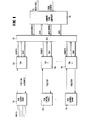
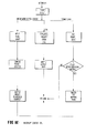
- FIG. 1 is a schematic illustration of the relevant portion of the TDMA circuit in a single ground station with which the present invention is concerned.
- a plurality of analog channels which may be comprised of simple telephone lines for example are input to an associated 1 out of n PCM channel banks 10a through 10n.
- Each PCM channel bank converts the parallel analog input signals to pulse code modulated (PCM) time division multiplexed (TDM) serial bit streams which are applied to an associated 1 out of n terrestrial interface modules (TIM) 15a through 15n.
- PCM pulse code modulated
- TDM time division multiplexed
- TIM terrestrial interface modules
- the common TDMA equipment 25 processes the data so provided and delivers it to a modulator.
- the processing involved in the common TDMA equipment and subsequent modulation does not represent a part of the subject invention.
- Data returning to the common TDMA equipment 25 from the demodulator is applied to the appropriate TIM module through bus 20 at the proper time.
- the appropriate TIM module is selected by the common equipment 25 by providing an address to all of the TIM modules simultaneously; the particular address so provided will cause the data to be written into only one of the TIM modules 15a through 15n.
- the data words provided to the TIM modules 15a through 15n are subsequently delivered to PCM channel banks 10a through lOn where they are demultiplexed and provided as a plurality of parallel analog signals from each of the channel banks.
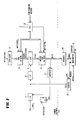
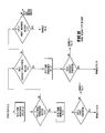
- Figure 2 illustrates the bus structure which provides a multiplex/demultiplex operation between a plurality of terrestrial interface modules (TIMs) and equipment common to each of the TIMs.
- the apparatus shown in Figure 2 is the receive side of the TDMA system.
- the transmit side of the TDMA system is exactly the same but for minor changes to be described below.
- a clock input of approximately 24 MHz is input to divide-by-16 counter 5.
- the output of counter 5 is applied to divide-by-12 counter 11 and to the clock input of counter 55.
- the output of counter 11 is applied to divide-by-3,072 counter 16 which is preset in accordance with CPU 21.
- the actual counter values depend upon system requirements such as the number of blocks per TDMA frame and are therefore a matter of choice.
- Burst counter 26 keeps a constant count of the burst presently being processed by the common equipment.
- the aperture signal which may be generated synchronously with each burst within the TDMA frame in any well-known manner, may alternatively be provided in accordance with the teachings of the co-pending, commonly assigned United States Patent Application Serial No. 79,619, entitled “Microprogrammable TDMA Terminal Controller” by Joseph Deal, concurrently filed herewith.
- the burst counter 26 delivers the number of bursts to the RAM network 35.
- Each of the bursts B 1 through Bn+1 is received by the receive portion of the common equipment.
- the unique word which supplies extremely fine synchronization information is extracted from each of the bursts in the common equipment by generating an aperture which is designed to surround the predicted occurrence in time of each unique word. With the unique word detection only performed during this aperture, the possibility of detecting false unique words is greatly reduced.
- a 96 bit "demand assignment request" follows the unique words in each of the ordinary station bursts. Following this 96 bit request is the data traffic containing the PCM channel information. Any station other than the central network controller will ignore the demand assignment request upon receipt and handle only the data traffic for that particular burst.
- the aperture signal is combined with the unique word detection signal in one of AND gates 220.
- Unique word detectors such as the one shown in Figure 7 are well-known in the art and may distinguish between a regular unique word contained in the ordinary station burst and an inverted unique word contained in the reference station burst.
- the unique word detector 215 may alternatively be provided by the controller disclosed in United States Patent Application Serial No. 79,619.
- flip-flop 225 Upon detection of the ordinary station unique word within the aperture, flip-flop 225 is set and enables counter 230 to count through the first 96 bits after the unique word.
- the bit rate clock input to counters 230 and 245 is supplied by the ground station modem.
- the flip-flop 235 After reaching the 96th bit, the flip-flop 235 is enabled to provide the "traffic start" signal to the flip-flop 45 in the common equipment of Figure 2.
- each "traffic start” signal defines a preselected position along a single TDMA frame.
- burst B 1 has a traffic start signal defined at position or block No. 0 while the second burst has its start signal at block No. 55, and so on.
- a maximum of 3,072 blocks are allowed within one TDMA frame.
- RAM 35 "knows" a priori the proper assigned position for each of the traffic start signals for each burst within the TDMA frame, and it needs only keep track of which burst is presently being processed.
- RAM 35 presets the block position "55" into divide-by-3,072 counter 16 before counter 5 is enabled by flip-flop 45 to count the 24 MHz clock.
- RAM 35 has address "...0010” applied to its address lines from counter 26 (burst 2), it outputs a "55" (binary) in order to preset counter 16.
- the block counter 16 is preset in this manner since proper generation of the aperture signal is of higher probability than proper generation of the traffic signal (unique word); it is much likely that the unique word will not be detected as opposed as not detecting the aperture signal. If the block counter 16 were not preset, upon missing a unique word, counter 5 would not be enabled, the number contained in block counter 16 would be inaccurate, and the mapping RAM 14 would supply improper information to each of the TIMs.
- RAM network 14 also knows a priori the number of data blocks contained in each burst and can therefore provide a signal to reset flip-flop 45 in order to disable counter 5 as soon as the entire burst has been accounted for. In this manner, the counter 16 will not erroneously count any more signals and provide an improper indication to RAM network 14.
- RAM 14 Upon recognizing that all of the blocks of data within any particular burst have been received, RAM 14 provides a predetermined output (such as all l's) to comparator 30. Comparator 30 recognizes the predetermined output and generates an end of burst (EOB) signal which resets flip-flop 45 to disable counter 5.
- EOB end of burst
- Mapping RAM 14 is programmed to recognize a particular block of data presently being processed by the common equipment and to provide an output to all of the TIMs which indicates to the TIMs which, if any, should receive the current block of data.
- the RAM 14 provides an 8 bit output to all of the TIM decoders 1-256. In other words, if counter 16 indicates that block "5" is being received and if block "5" must be delivered to TIM No. 8, the address input "...0101" to RAM 14 produces an output "...01000" to each of the decoders in the TIMs.
- the decoder 40 located in each TIM receives the 8 bit input and provides a high or low signal in response thereto.
- Decoder 40 can be comprised of purely combinatorial discrete logic or can be a read only memory.
- the decoder would provide an output which will either enable or disable the the data buffer 60 so that data can selectively be written into the TIM.
- Data is written into the buffer 60 in accordance with the address provided by counter 55.
- the counter is loaded with a preset number upon a proper decoding and starts to count concurrently with the enable signal provided to the data buffer from decoder 40.
- the counter 55 is as large as necessary to provide for as many blocks of data as required in each TIM.
- the transmit portion of the TDMA common equipment and the TIMs is the same as that shown in Figure 2 except that RAM 35 and burst counter 25 need not be provided since any one ground station only transmits within one burst.
- the apparatus shown in Figure 2 does, however, allow the ground station to produce a burst for each of a plurality of satellite transponders.
- the burst counter 25 is replaced with a transponder counter so that the RAMs 35 and 14 can keep track of the transponder to which they will transmit in real time.
- CPU 21 is connected to RAM networks 35 and 14 in order to provide real time demand assignment control for every channel in each of the ground station networks.
- RAM network 35 functions to simply provide an output representing a block location for the beginning of data traffic for any particular burst iù accordance with the address provided by burst counter 26.
- Mapping RAM 14 determines which block of data is currently being processed by receiving that information from counter 16 as a 12 bit address. In response to the block count provided at the RAM address, RAM 14 simply provides an 8 bit indication of which, if any, of the 256 TIMs is to receive the block of data.
- RAM 14 further functions to recognize the end of a burst based on its prior knowledge of the burst length and provide a preselected output to comparator 30 to disable any further counting. It can thus be seen that CPU 21, upon receiving new burst or block assignment information from a central control network, can provide new mapping functions to the RAMs 35 and 14 by simply reprogramming the RAMs to effect different burst and block assignments.
- FIG. 6 illustrates the organization of each of RAM networks 35 and 14.
- Counter 110 represents either burst counter 25 or divide-by-3,072 counter 16.
- the counter 110 provides the current count to one of RAMs 125 or 130 through multiplexers 115 or 120.
- the RAM 125 or 130 which receives the count from counter 110 is the RAM which is currently being used in real time by the common equipment to provide the mapping function.
- the output of one of RAMs 125 or 130 is delivered via multiplexer 135 to provide the output to either counter 16 or decoder 40.
- the RAM network can be updated in real time to effect a change in burst or block assignment by reprogramming the other of RAMs 125 or 130 by means of CPU 21 which provides an address line to multiplexers 115 and 120 and the data line to multiplexer 140.
- the address is provided to the other of RAMS 125 or 130 through multiplexers 115 or 120, respectively.
- the reprogrammed data from the CPU is provided to the other of RAMs 125 or 130 through multiplexer 140.
- the "ping-pong" control of the RAMs 125 and 130 is effected through the multiplexers 115, 120, 135 and 140 under the control of CPU 21.
- the CPU Upon the reprogramming of the other of RAMs 125 or 130, the CPU will effect a change of control on the "super frame" boundary (approximately 10 TDMA frames). The timing of the ping-pong action is however a matter of choice.
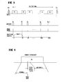
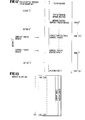
- each of the ground stations provides a single burst of data within the TDMA frame ( Figure 3).
- Each of the station burst contains a demand assignment request as shown in Figure 4.
- This request provides a central control network with information concerning channel usage at each station as well as requests from each station to either add or drop particular station channels.
- the central control network receives the demand assignment requests from each of the stations in the network in a well-known manner and provides an updated channel allocation assignment in accordance with a particular demand assignment algorithm.
- Two such demand assignment algorithms which may be applied to the present system are currently being used and are known as the "Demand Assigned Switching and Signaling System” (DASS) and the "Marisat (Maritime Satellite) TDMA Chaty System”.
- the central control network provides the reference station burst which brackets the TDMA frame as shown in Figure 3.
- Figure 5 illustrates the reference station burst in more detail.
- the reference burst is similar to the ordinary station burst insofar as it first provides a preamble, and a unique word. After the unique word is a "TDMA signaling message" which provides the reassignment information to each of the stations in the network.
- the unique word detector 215 detects the presence of the reference station burst by noting the inverted state of the unique word and enables the associated one of AND gates 220 in order to set flip-flop 240.
- Flip-flop 240 provides a signal to counter 245 which initializes that counter and causes it to begin a counting procedure.
- Counter 245 counts to a maximum of 1024 corresponding to the 1024 bits in the TDMA signalling message.
- the output of counter 245 provides a write address to the RAM 255 through address multiplexer 250 which is controlled by the output of flip-flop 240.
- the data bits from the reference burst are read into the RAM 255 at addresses designated by the counter 245.
- the flip-flop 240 is reset and address multiplexer 250 provides the read address to the RAM 255 through address multiplexer 250.
- the central network control signal that is, the TDMA signaling data, is delivered to the CPU 21.
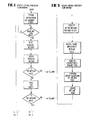
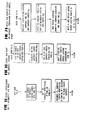
- FIG. 8-10 illustrate the receive control processor flow diagram.
- Figure 11 is the flow diagram for determining the type of frame management message.
- the bit error rate is also calculated.
- the BER has a direct relationship to the number of "1" bits counted. The BER is routed to the monitor and control processor (MCP) for transmission to the reference station.
- MCP monitor and control processor
- a parity check is performed on the decoded signaling message. If a parity error is found, the MCP is notified to enable it to direct the common equipment to enter phase 1 of the startup procedure.
- the transmission instant message for any particular station, arrives at a superframe rate. Once per superframe this message is sent to the CPU for position correction of the packet transmission. The remainder of the data is the frame management message which is decoded and evaluated by the CPU. If necessary, the off-line RAMs will be updated. Packet frame position control data contained in the frame management message are transferred to the CPU. Every ordinary station common equipment must maintain receive information concerning system status in order to calculate from the TDMA signaling message new packet ranks, and subpacket rank positions within individual data packets.
- packet is equivalent to "burst” as used above, the term “subpacket” is equivalent to “block” as used above, and the term “packet rank” refers to the number or position of a burst within a TDMA frame.
- the common equipment maintains system memory maps for calculating aperture arrivals and a receiver map for subpacket positions within data packets destined for local TIMs. These maps facilitate changing TIM subpacket addresses and aperture addresses in the respective mapping memories. Therefore, multiple algorithms are required to interpret the frames management message and configure terminal control units.
- Figure 12 shows the system memory map.
- Section A is comprised of the system and working registers.
- Section B is the packet rank section, and it is assigned a specific block of system memory locations.
- the first subpacket pointer address for each packet is stored in a packet location in system memory (Section B) according to the packet rank.
- Section B is comprised of 256 sub-blocks, one for each possible.network packet. This allows access to the first subpacket pointer for any packet by merely adding the packet rank to the address of the first packet location.
- Section C contains the subpacket pointer. The number of sub-blocks in Section C is determined by the number of packet and subpackets which are active at any given time.
- the subpacket pointers designate the locations in the receive control memories which contain the TIM addresses for each subpacket.
- the common equipment keeps an updated record of the location of each subpacket TIM address, subpacket rank in the packet, and corresponding packet rank in the frame.
- the fourth section (D) of system memory contains the aperture location map.
- the map contains the 256 possible aperture pointers. These aperture pointers designate the position in the aperture mapping memory of the frame position for each active aperture.
- Figure 13 shows the aperture memory map.
- the aperture memory When a data packet is generated, deleted or moved, the aperture memory must be updated. This is accomplished by using Section D of the system memory to locate the new frame position in the aperture memory. This may require the shifting of other apertures.
- the system memory maps, Section D keep an updated record of where the apertures are located in the aperture memory and thus allows for fast relocation of the frame position.
- the updating of the aperture memory is too slow to be accomplished in real time via the processor.
- the updating is done in an off-line RAM and switched in at the same time as the receive control memory.
- the flow charts of the algorithms of Figures 14-34 also contain the aperture generation procedure.
- the present invention thus teaches a technique of providing a multiplex-demultiplex function which uses a plurality of mapping RAMs to effect a compact and flexible bus structure for interfacing a plurality of TIMs with common TDMA equipment.
- the mapping function of the RAMs will not be seriously effected by the loss of a synchronization signal (unique word) in as much as the RAMs keep track of data block position and preset the data block count upon the occurrence of each new data burst.
- the subject invention further provides a technique of performing a demand assignment routine in real time by simply "re-mapping" one or both of the mapping RAMs providing the mapping function.
Landscapes
- Engineering & Computer Science (AREA)
- Signal Processing (AREA)
- Computer Networks & Wireless Communication (AREA)
- Time-Division Multiplex Systems (AREA)
- Radio Relay Systems (AREA)
- Small-Scale Networks (AREA)
- Mobile Radio Communication Systems (AREA)
- Use Of Switch Circuits For Exchanges And Methods Of Control Of Multiplex Exchanges (AREA)
Applications Claiming Priority (2)
| Application Number | Priority Date | Filing Date | Title |
|---|---|---|---|
| US06/079,655 US4298979A (en) | 1979-09-27 | 1979-09-27 | Decoding TIM bus structure |
| US79655 | 1979-09-27 |
Publications (3)
| Publication Number | Publication Date |
|---|---|
| EP0027006A2 true EP0027006A2 (de) | 1981-04-15 |
| EP0027006A3 EP0027006A3 (en) | 1981-07-08 |
| EP0027006B1 EP0027006B1 (de) | 1985-05-15 |
Family
ID=22151947
Family Applications (1)
| Application Number | Title | Priority Date | Filing Date |
|---|---|---|---|
| EP80303351A Expired EP0027006B1 (de) | 1979-09-27 | 1980-09-24 | Busstruktur mit dekodierenden, erdgebundenen Schnittstellenmoduln |
Country Status (6)
| Country | Link |
|---|---|
| US (1) | US4298979A (de) |
| EP (1) | EP0027006B1 (de) |
| JP (1) | JPS5696596A (de) |
| CA (1) | CA1155977A (de) |
| DE (1) | DE3070647D1 (de) |
| FR (1) | FR2466921B1 (de) |
Cited By (1)
| Publication number | Priority date | Publication date | Assignee | Title |
|---|---|---|---|---|
| EP0307962A2 (de) * | 1987-09-21 | 1989-03-22 | Nec Corporation | Rundfunkkommunikationssystem mit Mehrfachzugriff im Zeitmultiplex |
Families Citing this family (17)
| Publication number | Priority date | Publication date | Assignee | Title |
|---|---|---|---|---|
| US4382295A (en) * | 1981-04-23 | 1983-05-03 | Bell Telephone Laboratories, Incorporated | Digital conference time slot interchanger |
| JPS60239131A (ja) * | 1984-05-14 | 1985-11-28 | Nec Corp | Tdma衛星通信システムにおける状態情報伝送方式 |
| JPS612435A (ja) * | 1984-06-14 | 1986-01-08 | Nec Corp | 受信位置予測装置 |
| GB8505516D0 (en) * | 1985-03-04 | 1985-04-03 | British Telecomm | Interface circuit |
| JP2845889B2 (ja) * | 1988-05-16 | 1999-01-13 | 株式会社日立製作所 | 衛星通信方式及び衛星通信システム |
| US5574951A (en) * | 1993-03-17 | 1996-11-12 | Unisys Corporation | System for providing a time division random access including a high speed unidirectional bus and a plurality of function cards connected in a daisy chain |
| US5646947A (en) * | 1995-03-27 | 1997-07-08 | Westinghouse Electric Corporation | Mobile telephone single channel per carrier superframe lock subsystem |
| MY121893A (en) * | 1995-04-28 | 2006-03-31 | Qualcomm Inc | Method and apparatus for providing variable rate data in a communications system using statistical multiplexing. |
| US5859840A (en) * | 1996-05-31 | 1999-01-12 | Qualcomm Incorporated | Spread spectrum communication system which defines channel groups comprising selected channels that are additional to a primary channel and transmits group messages during call set up |
| US5726983A (en) * | 1996-08-09 | 1998-03-10 | Motorola, Inc. | Communication device with variable frame processing time |
| US6496543B1 (en) * | 1996-10-29 | 2002-12-17 | Qualcomm Incorporated | Method and apparatus for providing high speed data communications in a cellular environment |
| US6173007B1 (en) | 1997-01-15 | 2001-01-09 | Qualcomm Inc. | High-data-rate supplemental channel for CDMA telecommunications system |
| US6335922B1 (en) | 1997-02-11 | 2002-01-01 | Qualcomm Incorporated | Method and apparatus for forward link rate scheduling |
| US7751370B2 (en) * | 2001-07-13 | 2010-07-06 | Qualcomm Incorporated | Method and apparatus for forward link rate scheduling |
| KR100228318B1 (ko) * | 1997-03-14 | 1999-11-01 | 윤종용 | 다중 펄스코드 변조데이터 합성회로 |
| US6480521B1 (en) | 1997-03-26 | 2002-11-12 | Qualcomm Incorporated | Method and apparatus for transmitting high speed data in a spread spectrum communications system |
| US8116632B2 (en) * | 2007-11-30 | 2012-02-14 | Raytheon Company | Space-time division multiple-access laser communications system |
Citations (3)
| Publication number | Priority date | Publication date | Assignee | Title |
|---|---|---|---|---|
| GB1395512A (en) * | 1971-08-11 | 1975-05-29 | Post Office | Communications system |
| US3922496A (en) * | 1974-02-11 | 1975-11-25 | Digital Communications Corp | TDMA satellite communications system with guard band obviating ongoing propagation delay calculation |
| DE2647354A1 (de) * | 1975-10-20 | 1977-04-21 | Digital Communications Corp | Verfahren und einrichtung zur synchronisation von tdma-kommunikationsnetzen |
Family Cites Families (6)
| Publication number | Priority date | Publication date | Assignee | Title |
|---|---|---|---|---|
| US3632882A (en) * | 1970-05-15 | 1972-01-04 | Gen Datacomm Ind Inc | Synchronous programable mixed format time division multiplexer |
| US3927268A (en) * | 1971-04-30 | 1975-12-16 | Communications Satellite Corp | Speech predictive encoding communication system |
| US3806879A (en) * | 1971-08-11 | 1974-04-23 | Communications Satellite Corp | Tdma satellite communication system with multi-pcm frames per tdma frame |
| US4048447A (en) * | 1974-03-15 | 1977-09-13 | Nippon Electric Company, Limited | PCM-TASI signal transmission system |
| CH577253A5 (de) * | 1974-05-17 | 1976-06-30 | Ibm | |
| US4205200A (en) * | 1977-10-04 | 1980-05-27 | Ncr Corporation | Digital communications system utilizing controllable field size |
-
1979
- 1979-09-27 US US06/079,655 patent/US4298979A/en not_active Expired - Lifetime
-
1980
- 1980-01-02 FR FR8000016A patent/FR2466921B1/fr not_active Expired
- 1980-09-09 CA CA000359922A patent/CA1155977A/en not_active Expired
- 1980-09-24 DE DE8080303351T patent/DE3070647D1/de not_active Expired
- 1980-09-24 EP EP80303351A patent/EP0027006B1/de not_active Expired
- 1980-09-27 JP JP13509180A patent/JPS5696596A/ja active Pending
Patent Citations (3)
| Publication number | Priority date | Publication date | Assignee | Title |
|---|---|---|---|---|
| GB1395512A (en) * | 1971-08-11 | 1975-05-29 | Post Office | Communications system |
| US3922496A (en) * | 1974-02-11 | 1975-11-25 | Digital Communications Corp | TDMA satellite communications system with guard band obviating ongoing propagation delay calculation |
| DE2647354A1 (de) * | 1975-10-20 | 1977-04-21 | Digital Communications Corp | Verfahren und einrichtung zur synchronisation von tdma-kommunikationsnetzen |
Cited By (2)
| Publication number | Priority date | Publication date | Assignee | Title |
|---|---|---|---|---|
| EP0307962A2 (de) * | 1987-09-21 | 1989-03-22 | Nec Corporation | Rundfunkkommunikationssystem mit Mehrfachzugriff im Zeitmultiplex |
| EP0307962A3 (en) * | 1987-09-21 | 1990-05-16 | Nec Corporation | Time division multiple access radio communication system |
Also Published As
| Publication number | Publication date |
|---|---|
| DE3070647D1 (en) | 1985-06-20 |
| FR2466921A1 (fr) | 1981-04-10 |
| CA1155977A (en) | 1983-10-25 |
| FR2466921B1 (fr) | 1985-11-29 |
| EP0027006B1 (de) | 1985-05-15 |
| US4298979A (en) | 1981-11-03 |
| EP0027006A3 (en) | 1981-07-08 |
| JPS5696596A (en) | 1981-08-04 |
Similar Documents
| Publication | Publication Date | Title |
|---|---|---|
| US4298979A (en) | Decoding TIM bus structure | |
| US4507781A (en) | Time domain multiple access broadcasting, multipoint, and conferencing communication apparatus and method | |
| US4700341A (en) | Stochastic time division multiplexing | |
| US5202885A (en) | Atm exchange with copying capability | |
| US4771425A (en) | Synchoronous packet voice/data communication system | |
| US3796835A (en) | Switching system for tdm data which induces an asynchronous submultiplex channel | |
| US4328543A (en) | Control architecture for a communications controller | |
| US5274680A (en) | Device for the transmission of synchronous information by an asynchronous network, notably an ATM network | |
| US4903261A (en) | Synchronous packet voice/data communication system | |
| US4819228A (en) | Synchronous packet voice/data communication system | |
| US4332026A (en) | Multiple data rate digital switch for a TDMA communications controller | |
| US5434859A (en) | Transmission system for transmitting information at various rates and transmitter station and receiver station suitable for such a system | |
| CA1143879A (en) | Priority threaded message burst mechanism for tdma communication | |
| US4532625A (en) | Communications network status information system | |
| US4315330A (en) | Multiple data rate testing of communication equipment | |
| CA2042037C (en) | Multiple access system for a communication network | |
| EP0114678A2 (de) | Basisbandanlage für eine Erdfunkstelle eines mit Vielfachzugriff im Zeitmultiplex arbeitenden Satellitenübertragungssystems | |
| JPS6258577B2 (de) | ||
| US3904829A (en) | Demand driven multiplexing system | |
| US4307461A (en) | Call processor for a satellite communications controller | |
| US3732548A (en) | Switching center for a data network | |
| US4546470A (en) | Communications systems | |
| US4418409A (en) | Byte data activity compression | |
| US4320504A (en) | Mechanism for synchronization of data ports in TDMA communication | |
| EP0899899B1 (de) | Gerät und Verfahren zur Teilung eines Signalisierungskanals |
Legal Events
| Date | Code | Title | Description |
|---|---|---|---|
| PUAI | Public reference made under article 153(3) epc to a published international application that has entered the european phase |
Free format text: ORIGINAL CODE: 0009012 |
|
| AK | Designated contracting states |
Designated state(s): BE DE GB IT NL SE |
|
| PUAL | Search report despatched |
Free format text: ORIGINAL CODE: 0009013 |
|
| RHK1 | Main classification (correction) |
Ipc: H04B 7/185 |
|
| AK | Designated contracting states |
Designated state(s): BE DE GB IT NL SE |
|
| 17P | Request for examination filed |
Effective date: 19811224 |
|
| ITF | It: translation for a ep patent filed | ||
| GRAA | (expected) grant |
Free format text: ORIGINAL CODE: 0009210 |
|
| AK | Designated contracting states |
Designated state(s): BE DE GB IT NL SE |
|
| REF | Corresponds to: |
Ref document number: 3070647 Country of ref document: DE Date of ref document: 19850620 |
|
| PGFP | Annual fee paid to national office [announced via postgrant information from national office to epo] |
Ref country code: NL Payment date: 19850930 Year of fee payment: 6 |
|
| PLBE | No opposition filed within time limit |
Free format text: ORIGINAL CODE: 0009261 |
|
| STAA | Information on the status of an ep patent application or granted ep patent |
Free format text: STATUS: NO OPPOSITION FILED WITHIN TIME LIMIT |
|
| 26N | No opposition filed | ||
| PG25 | Lapsed in a contracting state [announced via postgrant information from national office to epo] |
Ref country code: SE Effective date: 19860925 |
|
| PG25 | Lapsed in a contracting state [announced via postgrant information from national office to epo] |
Ref country code: BE Effective date: 19860930 |
|
| BERE | Be: lapsed |
Owner name: COMMUNICATIONS SATELLITE CORP. Effective date: 19860930 |
|
| PG25 | Lapsed in a contracting state [announced via postgrant information from national office to epo] |
Ref country code: NL Effective date: 19870401 |
|
| NLV4 | Nl: lapsed or anulled due to non-payment of the annual fee | ||
| PG25 | Lapsed in a contracting state [announced via postgrant information from national office to epo] |
Ref country code: DE Effective date: 19870602 |
|
| GBPC | Gb: european patent ceased through non-payment of renewal fee | ||
| PG25 | Lapsed in a contracting state [announced via postgrant information from national office to epo] |
Ref country code: GB Effective date: 19881118 |
|
| EUG | Se: european patent has lapsed |
Ref document number: 80303351.3 Effective date: 19870812 |