EP0024236B1 - Procédé de transcodage d'informations pour transmission sur ligne et système de transmission l'utilisant - Google Patents
Procédé de transcodage d'informations pour transmission sur ligne et système de transmission l'utilisant Download PDFInfo
- Publication number
- EP0024236B1 EP0024236B1 EP19800401159 EP80401159A EP0024236B1 EP 0024236 B1 EP0024236 B1 EP 0024236B1 EP 19800401159 EP19800401159 EP 19800401159 EP 80401159 A EP80401159 A EP 80401159A EP 0024236 B1 EP0024236 B1 EP 0024236B1
- Authority
- EP
- European Patent Office
- Prior art keywords
- code
- words
- information
- sum
- symbols
- Prior art date
- Legal status (The legal status is an assumption and is not a legal conclusion. Google has not performed a legal analysis and makes no representation as to the accuracy of the status listed.)
- Expired
Links
- 230000005540 biological transmission Effects 0.000 title claims description 27
- 238000000034 method Methods 0.000 title claims description 23
- 238000006243 chemical reaction Methods 0.000 title description 2
- 230000009466 transformation Effects 0.000 claims description 10
- 238000010586 diagram Methods 0.000 description 53
- 230000033764 rhythmic process Effects 0.000 description 24
- 230000015654 memory Effects 0.000 description 13
- 230000003595 spectral effect Effects 0.000 description 10
- 230000001360 synchronised effect Effects 0.000 description 8
- 239000004020 conductor Substances 0.000 description 6
- 238000001228 spectrum Methods 0.000 description 6
- 238000007493 shaping process Methods 0.000 description 5
- 238000011084 recovery Methods 0.000 description 4
- 238000005070 sampling Methods 0.000 description 4
- 230000008901 benefit Effects 0.000 description 3
- 230000015556 catabolic process Effects 0.000 description 2
- 238000001514 detection method Methods 0.000 description 2
- 241001080024 Telles Species 0.000 description 1
- KZSNJWFQEVHDMF-UHFFFAOYSA-N Valine Chemical compound CC(C)C(N)C(O)=O KZSNJWFQEVHDMF-UHFFFAOYSA-N 0.000 description 1
- 230000003321 amplification Effects 0.000 description 1
- 238000013459 approach Methods 0.000 description 1
- 238000007796 conventional method Methods 0.000 description 1
- 238000006731 degradation reaction Methods 0.000 description 1
- 238000011161 development Methods 0.000 description 1
- 230000008030 elimination Effects 0.000 description 1
- 238000003379 elimination reaction Methods 0.000 description 1
- 230000002349 favourable effect Effects 0.000 description 1
- 239000000835 fiber Substances 0.000 description 1
- 230000004907 flux Effects 0.000 description 1
- 239000000463 material Substances 0.000 description 1
- 238000003199 nucleic acid amplification method Methods 0.000 description 1
- 239000013307 optical fiber Substances 0.000 description 1
- 230000008569 process Effects 0.000 description 1
- 230000004044 response Effects 0.000 description 1
- 238000012552 review Methods 0.000 description 1
- 230000001131 transforming effect Effects 0.000 description 1
Images


Classifications
-
- H—ELECTRICITY
- H04—ELECTRIC COMMUNICATION TECHNIQUE
- H04L—TRANSMISSION OF DIGITAL INFORMATION, e.g. TELEGRAPHIC COMMUNICATION
- H04L25/00—Baseband systems
- H04L25/38—Synchronous or start-stop systems, e.g. for Baudot code
- H04L25/40—Transmitting circuits; Receiving circuits
- H04L25/49—Transmitting circuits; Receiving circuits using code conversion at the transmitter; using predistortion; using insertion of idle bits for obtaining a desired frequency spectrum; using three or more amplitude levels ; Baseband coding techniques specific to data transmission systems
- H04L25/4917—Transmitting circuits; Receiving circuits using code conversion at the transmitter; using predistortion; using insertion of idle bits for obtaining a desired frequency spectrum; using three or more amplitude levels ; Baseband coding techniques specific to data transmission systems using multilevel codes
- H04L25/4923—Transmitting circuits; Receiving circuits using code conversion at the transmitter; using predistortion; using insertion of idle bits for obtaining a desired frequency spectrum; using three or more amplitude levels ; Baseband coding techniques specific to data transmission systems using multilevel codes using ternary codes
- H04L25/4925—Transmitting circuits; Receiving circuits using code conversion at the transmitter; using predistortion; using insertion of idle bits for obtaining a desired frequency spectrum; using three or more amplitude levels ; Baseband coding techniques specific to data transmission systems using multilevel codes using ternary codes using balanced bipolar ternary codes
Definitions
- the present invention relates to the field of information transcoding and it relates more particularly to a method of transforming a flow of information, binary for example, into a pulse flow better suited to the usual transmission media (cable with metallic conductor, fiber optic cable, etc.).
- the invention also relates to a transmission system allowing the implementation of this method.
- this criterion is the current numerical sum, of which recalls that it is the sum of the values of the symbols of the code between the instant chosen as the origin of the emission and any instant.
- the bounding of the digital sum makes it possible in particular to eliminate the continuous component of the transmitted signal: the coding law therefore generally regulates the passage from one alphabet to another in order to reduce the current digital sum .
- the present invention aims to reduce the width of the frequency spectrum used for the transmission of information compared to that of the usual codes. This is achieved by delimiting the alternating sum, i.e. the sum of the values of the symbols of even rank minus the sum of the symbols of odd rank of the same code, between the instant chosen as the origin of the broadcast and any moment.
- the invention also relates to an information transmission system allowing the implementation of the above method and for this purpose comprises a transmission module and a reception module placed on either side of a line. of transmission.
- the first implementation of the invention uses a particular transcoding of the so-called 1 B / 2T type, in which the information to be transmitted is expressed in binary form and the transcoded information, transmitted on the transmission channel, is expressed in form of words of two ternary symbols, that is to say can take one of three values, usually represented by the symbols: "O" "+” and "-"
- This code is called 1 B / 2T 4E 3S1 3M, where 3 and 1 are the limits of the variations of the current and alternate sums and 3M means that it contains three prohibited words.
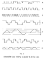
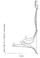
- the diagrams in FIG. 1 show the binary signal carrying the information to be transmitted in A respectively, in B the clock signal defining the rhythm of the binary signal, in C the clock signal defining the rhythm of the signal transcoded; this signal C is at double frequency of the signal B.
- the diagram D represents the transcoded signal corresponding to the information A using the alphabet of table 1 and an internal logic of the coder explained below. As it appears, each of the binary symbols of the information can be associated with a ternary word of two symbols chosen from four possible words.
- the diagram F is deduced from the diagram D by changing the sign of the second symbol of each ternary word and makes it possible to calculate the alternating sum.
- the choice of the alphabet is made according to the value of the signal E at the end of the ternary word, according to the law in Table 2.
- the internal states of the encoder are none other than the conventional representation of the pairs of possible values of the curves E and G at the end of the transcoded word.
- the multiplier of error for this code is 0.59.
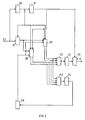
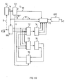
- FIG. 2 is a block diagram of the coder used in the previous example.
- the input of the coder to which the binary information to be transmitted is applied is represented in EB.
- Diagram A of FIG. 1 is shown in ST.
- the output terminal on which the ternary signal intended for transmission on the line is delivered is shown in ST. diagram D).
- 10 shows a clock reproducing the rhythm frequency of the binary input information. This clock can be synchronized by the signal itself, as represented by the broken line 9, or by any other external means.
- the clock 10 delivers the signal represented by the diagram B in FIG. 1; it feeds a binary multiplier 11 ensuring a multiplication by two.
- the output signal of the multiplier 11 corresponds to diagram C of FIG. 1.
- the input signal is applied in parallel to one of the terminals of each of two address generator circuits, respectively 12 and 13, associated respectively with read-only memories 14 and 15.
- memory 14 are stored the permitted code words of the alphabets as defined in table 1.
- the selected code word is transmitted via parallel-series registers 16 and 17 and a summing circuit 20 at the output ST.
- the registers 16 and 17 are synchronized respectively by the clock 10 and the circuit 11 for recording and reading.
- These signals control the choice of the code word used from the four alphabets defined in Table 1, taking into account the code word which has just been transmitted, so that the condition B + B 's 4 to which the code obeys is respected . It constitutes what has been designated above by “internal logic of the coder. This internal logic is defined by Tables 2 and 3.
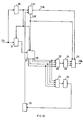
- FIG. 3 is a block diagram of the decoder corresponding to the coder of FIG. 2.
- the input of the decoder connected to the transmission line, receiving the transmitted ternary signal, has been shown at AND.
- the rhythm frequency of this signal is reconstituted in the clock 30 which supplies on the one hand a regenerator 31 and, on the other hand, a frequency divider circuit 21 restoring the rhythm of the binary information.
- the regenerator 31 includes in particular, as is well known, circuits equalization and amplification of the received signal. Its implementation is not modified by the coding method according to the invention.
- the amplified ternary signal is applied to registers 26 and 27 series-parallel, synchronized by the circuit 21 and the clock 30 so as to restore the division into ternary words of two symbols.
- the memory 24 delivers (output SB) the binary information corresponding to the word applied to the generator 22, by l 'through a shaping circuit 29 synchronized by the clock 21, this shaping being done by sampling.
- the address generator 23 supplies the read-only memory 25 for recognizing prohibited words which, via the synchronization circuit 28, controls the registers 26 and 27. In fact, words comprising two symbols are cut out in the continuous ternary sequence transmitted by line; the output information from registers 26 and 27 is a ternary word of two symbols which can either belong to two successive words, or to the same word.
- the words formed correspond to forbidden words which, via the elements 23 and 25, control the synchronization circuit of the registers 26 and 27, advancing the registers by an elementary time.
- the words reconstituted by the registers belong to an alphabet of the code and correspond to binary information transmitted by the set 22, 24 and 29 at the output SB. It is obvious that the increase in the number of prohibited words facilitates synchronization.
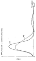
- FIG. 4 represents the spectral densities, that is to say the amplitude responses for a binary train of constant amplitude, on the one hand of the code which has just been defined (solid line 41) and for the purposes of comparison, the frequency spectrum of the AMI (Alternate Mark Inversion) code (broken line 42).
- AMI Alternate Mark Inversion
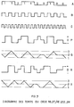
- the binary sequence A corresponds to the code represented by the diagram H.
- the diagrams B and C respectively represent the rhythms of the binary and ternary signals.
- Diagram H represents the coded signal, the diagram I the integral of H.
- the diagram J is derived from the diagram H by inverting the second symbol of each ternary word and the diagram K is the integral of the diagram J.
- FIGS. 6 and 7 respectively represent the same variables for two other codes according to the invention, the code 1 B / 2T 4E 2S2 3M, differing from the previous one by the number of forbidden words which becomes three instead of one, and the code 1 B / 2T 4E 2S2 2M in which the number of prohibited words is two.
- the invention is more generally applicable to codes of the nB / mT type, n and m being any integers.
- the invention is not limited to transcoding from binary to ternary, but also applies to binary-binary transcoding, of the so-called nB / mB type.
- a code of the type 3B / 4B called 3B / 4B 4E 6S6 OM, comprising four alphabets is described below, for which the maximum variation of the numerical sum (B) and of the alternating sum (B ') is equal to 6, and having no prohibited word, which gives a better performance for the code but complicates the decoding, as is known.
- the conversion table is reproduced in table 7 for coding and table 2 for decoding.
- the internal logic of the coder is defined by the last right column of table 7 which fixes the rank of the alphabet to be used for coding the next word.
- the signs + and - appearing in these tables corresponding to the values 1 and 0 assigned to the two binary symbols.
- FIG. 9 show, respectively at A the binary input signal, at B the clock signal defining the rhythm of the input bit stream, at C the clock signal defining the rhythm of the flow transcoded, which is at 4/3 frequency of signal B.
- Diagram D represents a synchronization signal common to clocks B and C.
- Diagram P represents the coded signal corresponding to information A using the alphabets of table 7 and the internal logic of the encoder explained in the last column on the right. As it appears, each of the eight binary words of three symbols of the bit stream to be coded is associated with a binary word of four symbols chosen from four possible alphabets. The choice of the alphabet used is made, from the code word previously used, to take account of the conditions imposed on the variations of the numerical sum and of the alternating sum.
- Diagram Q integral of diagram P
- B 6
- the diagram R is deduced from the diagram P by changing the sign of the second symbol of each transcoded word and makes it possible to calculate the alternating sum.
- FIG. 10 is a block diagram of the coder similar to that of FIG. 2 but adapted to the example above.
- the input of the coder to which the input bit stream to be transcoded is shown in EB is represented (diagram A in FIG. 9) and in SC the output terminal on which the bit stream transcoded at 4/3 rhythm is delivered the rate of the input bit stream, intended for transmission on the line (diagram P).
- the clock representing the rhythm frequency of the input bit stream is shown at 10. This clock can be synchronized by the signal itself, as represented by the broken line 9, or by any other external means.
- the clock 10 delivers the signal represented by the diagram B in FIG. 9. This signal is transmitted by the conductor 18 ′ to the parallel-series register 17 as well as to a series-parallel register 116.
- the clock 10 supplies a multiplier binary 111 ensuring a multiplication by 4/3.
- the output signal of the multiplier 111, transmitted by the conductor 18 to the register 17, corresponds to diagram C of FIG. 9.
- the multiplier 111 delivers by a conductor 18 "a signal for splitting the input bit stream EB into words of three symbols (diagram D in FIG. 9).
- This word cutting or synchronization signal is applied to the register 17.
- the word synchronization signal is also applied to the delay circuit 19.
- the input stream EB is transformed, in the serial-parallel register 116 supplying in parallel the two address generating circuits, respectively 12 and 13, associated respectively with the read-only memories 14 and 15 in a series of words of three symbols.
- In the memory 14 are stored the alphabets of code words as defined for example in table 7.
- the selected code word is transmitted via the parallel-series register 17 and a shaping circuit 120 to the output SC.
- the memory 15 are recorded the signs to those of the address generators 12 and 13 applied to them via the delay circuit 19 introducing a delay equal to the duration of a code word.
- These circuits ensure the selection of the alphabet according to the law appearing in the last right column of table 7 and constitute the "internal logic of the coder.
- the circuit 19 receives the word synchronization signal (D FIG. 9) to respect the phasing of the chopping.
- FIG. 11 is a block diagram of the decoder similar to that of FIG. 3 but corresponding to the coder of FIG. 10.
- the input of the decoder, connected to the transmission line receiving the transcoded bit stream, has been shown in EC.
- the rhythm frequency of this line signal is reconstituted in the clock 30 which supplies on the one hand the regenerator 31 and, on the other hand, a frequency divider circuit by 3/4, 121, restoring the rhythm of the bit stream on the output feeding a conductor 126 and the rhythm of the words 1/4 of the line rhythm) on the output feeding a conductor 126 '.
- the regenerator 31 notably includes circuits for equalizing and amplifying the line signal.
- the regenerated transcoded bit stream is applied to the serial-parallel register 27 synchronized by the elements 121 and 30 so as to reconstruct the code words of four symbols.
- code words are applied to the two address generators 22 and 23 associated with the two read-only memories 24 and 25.
- the memory 24 delivers to the output SB the binary word of three symbols corresponding to the code word applied at 22, according to the correspondence appearing for example in Table 8, by means of a shaping circuit 29 synchronized by the clock 21 of the bit stream rhythm, this shaping being done by sampling.
- the address generator 23 supplies the memory 25 for decoding information necessary for the recovery of synchronization of the words of the code: phasing of the division of the transmitted stream into words of four symbols. It is provided by the delay circuit 28 which controls the circuit 21 and more particularly the signal appearing on 26 '. Indeed, the online bit stream is continuous.
- the associated symbols can either belong to two successive words, or to the same word (phasing of the division into words of the transmitted bit stream).
- certain words formed correspond to forbidden words which, via 23 and 25, control the circuit 28 synchronizing the register 27, making the register advance by an elementary time by the clock 21.
- the words reconstituted by the register all belong to an alphabet of the code and correspond to a binary word decoded with three symbols transmitted by the set 22, 24 and 29 at the output SB. It is obvious that the increase in the number of prohibited words facilitates synchronization.
- the phasing of the division into words of four symbols is carried out by reconstitution in the synchronization member 28 of the internal states of the coder of FIG. 10.
- the signal leaving 25 then indicates the sum current of the received word; 28 thus controls the current and alternating sums of the flux received, at the instants of phasing, and ensures that the limits B and B 'are not exceeded.
- FIG. 12 represents at 141 the distribution of the spectral density of the code defined by Tables 7 and 8.
- the abscissa axis is graduated in normalized frequency (relation to the binary rhythm of the signal to be coded).
- the spectral density corresponding to code 5B-6B used in particular in transmission over optical fiber has been shown at 142.
- the figure clearly shows the advantages of the code according to the invention: higher density between 0 and 2/3 - zero energy at 2/3, 4/3, etc. while the first zero of the code 5B-6B is at 6/5.
- Examination of curve 141 shows that the bandwidth allocated to the transmission of the coded signals according to the invention can, despite the increase in the rate, be limited to the standardized frequency band 0-2 / 3. Under these conditions, an error on the bit stream of the line causes on average 1.443 error on the decoded bit stream.
- This code has maximum performance since all the words in the code are used.
- the curves correspond to an equiprobability of the two symbols in the stream to be coded. If we vary the probability of the binary symbols at the input of the coder, we notice that the spectrum of the code varies little. The code is therefore only very insensitive to the distribution of the bit stream and the economy of a jamming member is possible in equipment where this code is used.
- the frequency spectrum of the codes according to the invention does not have a continuous component. It also has a concentration of energy between the frequency zero and the first zero following, a concentration before two thirds of the input binary frequency, which is an advantage over previous binary codes, even the most economical in width of tape.
- the frequency spectrum of the preferred code variants according to the invention is relatively insensitive to the distribution of binary symbols in the information to be transmitted.
Landscapes
- Physics & Mathematics (AREA)
- Spectroscopy & Molecular Physics (AREA)
- Engineering & Computer Science (AREA)
- Computer Networks & Wireless Communication (AREA)
- Signal Processing (AREA)
- Compression, Expansion, Code Conversion, And Decoders (AREA)
- Dc Digital Transmission (AREA)
Applications Claiming Priority (2)
| Application Number | Priority Date | Filing Date | Title |
|---|---|---|---|
| FR7920063 | 1979-08-06 | ||
| FR7920063A FR2463542A1 (fr) | 1979-08-06 | 1979-08-06 | Procede de codage ternaire d'informations binaires pour transmission sur ligne et systeme de transmission l'utilisant |
Publications (2)
| Publication Number | Publication Date |
|---|---|
| EP0024236A1 EP0024236A1 (fr) | 1981-02-25 |
| EP0024236B1 true EP0024236B1 (fr) | 1983-09-14 |
Family
ID=9228641
Family Applications (1)
| Application Number | Title | Priority Date | Filing Date |
|---|---|---|---|
| EP19800401159 Expired EP0024236B1 (fr) | 1979-08-06 | 1980-08-06 | Procédé de transcodage d'informations pour transmission sur ligne et système de transmission l'utilisant |
Country Status (3)
| Country | Link |
|---|---|
| EP (1) | EP0024236B1 (oth) |
| DE (1) | DE3064824D1 (oth) |
| FR (1) | FR2463542A1 (oth) |
Families Citing this family (1)
| Publication number | Priority date | Publication date | Assignee | Title |
|---|---|---|---|---|
| US4486740A (en) * | 1982-12-06 | 1984-12-04 | At&T Bell Laboratories | DC Cancellation in ternary-coded data systems |
Family Cites Families (4)
| Publication number | Priority date | Publication date | Assignee | Title |
|---|---|---|---|---|
| US3215779A (en) * | 1961-02-24 | 1965-11-02 | Hallicrafters Co | Digital data conversion and transmission system |
| US3302193A (en) * | 1964-01-02 | 1967-01-31 | Bell Telephone Labor Inc | Pulse transmission system |
| US3587088A (en) * | 1967-12-21 | 1971-06-22 | Bell Telephone Labor Inc | Multilevel pulse transmission systems employing codes having three or more alphabets |
| GB1539389A (en) * | 1975-12-30 | 1979-01-31 | Standard Telephones Cables Ltd | Data transmission |
-
1979
- 1979-08-06 FR FR7920063A patent/FR2463542A1/fr active Granted
-
1980
- 1980-08-06 EP EP19800401159 patent/EP0024236B1/fr not_active Expired
- 1980-08-06 DE DE8080401159T patent/DE3064824D1/de not_active Expired
Also Published As
| Publication number | Publication date |
|---|---|
| FR2463542B1 (oth) | 1983-10-07 |
| FR2463542A1 (fr) | 1981-02-20 |
| DE3064824D1 (en) | 1983-10-20 |
| EP0024236A1 (fr) | 1981-02-25 |
Similar Documents
| Publication | Publication Date | Title |
|---|---|---|
| EP0481549B1 (fr) | Système et procédé de codage/décodage de signaux numériques transmis en modulation codée | |
| FR2471109A1 (fr) | Magnetoscope numerique | |
| FR2880482A1 (fr) | Dispositif de conversion d'un signal transmis en un signal numerique | |
| FR2794915A1 (fr) | Procede et dispositif d'emission, procede et dispositif de reception, et systemes les mettant en oeuvre | |
| FR2476943A1 (fr) | Procede et appareil pour transmettre des donnees dans un format de correction d'erreur | |
| EP0053958A1 (fr) | Procédé de transcodage parallèle série d'un train numérique parallèle | |
| EP0188030B1 (fr) | Procédé de codage et de décodage d'informations audio et appareil pour sa mise en oeuvre | |
| EP0024236B1 (fr) | Procédé de transcodage d'informations pour transmission sur ligne et système de transmission l'utilisant | |
| EP0711049A1 (fr) | Procédé de détection de symboles de référence pour récepteur de données numériques | |
| CH640678A5 (fr) | Procede et installation de transmission simultanee d'une onde basse frequence et d'un signal numerique mic. | |
| EP0228528A1 (fr) | Dispositif de mise en oeuvre d'un code à faible disparité accumulée en transmission numérique à haut débit et procédé de codage utilisant un tel dispositif | |
| EP0196979B1 (fr) | Procédé et dispositif d'insertion d'un signal numérique sur une voie à débit plus élevé | |
| EP1094631A1 (fr) | Recherche de l'instant d'échantillonnage optimal dans un système de transmissions par paquets TDMA | |
| CA2125444A1 (fr) | Systeme de transmission numerique a etalement de spectre obtenu par codage pseudo-aleatoire basse frequence de l'information utile et procede d'etalement et de compression de spectre utilise dans un tel systeme | |
| FR2522908A1 (fr) | Procede de transmission d'une voie de service, susceptible d'etre modifiee en cours de transmission, emetteur et recepteur pour la mise en oeuvre d'un tel procede | |
| EP0229738B1 (fr) | Procédé et dispositif de régénération de l'intégrité du débit binaire dans un réseau plésiochrone | |
| EP0045680A1 (fr) | Procédé de transcodage d'informations et système de transmission utilisant un tel procédé | |
| FR2613893A1 (fr) | Procede de commutation de signaux numeriques asynchrones, et dispositif pour la mise en oeuvre de ce procede | |
| WO1999001967A1 (fr) | Modulation multiporteuse employant des fonctions prototypes ponderees | |
| EP0083998A1 (fr) | Générateur d'octets chiffrants ou déchiffrants | |
| EP1050987A1 (fr) | Procédé d'accès multiple de type CDMA à capacité améliorée | |
| FR2472310A1 (fr) | Procede de transcodage d'informations binaires pour transmission sur ligne et systeme de transmission l'utilisant | |
| FR2800951A1 (fr) | Estimation de l'instant d'echantillonnage optimal dans un systeme de transmissions par paquets tdma | |
| FR2533093A1 (fr) | Procede de codage d'un flux de bits d'information, dispositif de mise en oeuvre de ce procede et dispositif de decodage d'un flux de bits d'information | |
| FR2798025A1 (fr) | Appareil de reception pour decoder un signal serie en signal d'informations et systeme de communication muni de l'appareil de reception |
Legal Events
| Date | Code | Title | Description |
|---|---|---|---|
| PUAI | Public reference made under article 153(3) epc to a published international application that has entered the european phase |
Free format text: ORIGINAL CODE: 0009012 |
|
| AK | Designated contracting states |
Designated state(s): CH DE GB NL SE |
|
| 17P | Request for examination filed |
Effective date: 19810317 |
|
| GRAA | (expected) grant |
Free format text: ORIGINAL CODE: 0009210 |
|
| AK | Designated contracting states |
Designated state(s): CH DE GB LI NL SE |
|
| REF | Corresponds to: |
Ref document number: 3064824 Country of ref document: DE Date of ref document: 19831020 |
|
| PLBE | No opposition filed within time limit |
Free format text: ORIGINAL CODE: 0009261 |
|
| STAA | Information on the status of an ep patent application or granted ep patent |
Free format text: STATUS: NO OPPOSITION FILED WITHIN TIME LIMIT |
|
| 26N | No opposition filed | ||
| PGFP | Annual fee paid to national office [announced via postgrant information from national office to epo] |
Ref country code: DE Payment date: 19940526 Year of fee payment: 15 |
|
| PGFP | Annual fee paid to national office [announced via postgrant information from national office to epo] |
Ref country code: SE Payment date: 19940527 Year of fee payment: 15 Ref country code: CH Payment date: 19940527 Year of fee payment: 15 |
|
| PGFP | Annual fee paid to national office [announced via postgrant information from national office to epo] |
Ref country code: GB Payment date: 19940531 Year of fee payment: 15 |
|
| PGFP | Annual fee paid to national office [announced via postgrant information from national office to epo] |
Ref country code: NL Payment date: 19940831 Year of fee payment: 15 |
|
| EAL | Se: european patent in force in sweden |
Ref document number: 80401159.1 |
|
| PG25 | Lapsed in a contracting state [announced via postgrant information from national office to epo] |
Ref country code: GB Effective date: 19950806 |
|
| PG25 | Lapsed in a contracting state [announced via postgrant information from national office to epo] |
Ref country code: SE Effective date: 19950807 |
|
| PG25 | Lapsed in a contracting state [announced via postgrant information from national office to epo] |
Ref country code: LI Effective date: 19950831 Ref country code: CH Effective date: 19950831 |
|
| PG25 | Lapsed in a contracting state [announced via postgrant information from national office to epo] |
Ref country code: NL Effective date: 19960301 |
|
| GBPC | Gb: european patent ceased through non-payment of renewal fee |
Effective date: 19950806 |
|
| REG | Reference to a national code |
Ref country code: CH Ref legal event code: PL |
|
| NLV4 | Nl: lapsed or anulled due to non-payment of the annual fee |
Effective date: 19960301 |
|
| PG25 | Lapsed in a contracting state [announced via postgrant information from national office to epo] |
Ref country code: DE Effective date: 19960501 |
|
| EUG | Se: european patent has lapsed |
Ref document number: 80401159.1 |