EP0020255B1 - Niveau de commutation d'un opérateur pour réseau de commutation de données numériques par paquets - Google Patents
Niveau de commutation d'un opérateur pour réseau de commutation de données numériques par paquets Download PDFInfo
- Publication number
- EP0020255B1 EP0020255B1 EP19800400728 EP80400728A EP0020255B1 EP 0020255 B1 EP0020255 B1 EP 0020255B1 EP 19800400728 EP19800400728 EP 19800400728 EP 80400728 A EP80400728 A EP 80400728A EP 0020255 B1 EP0020255 B1 EP 0020255B1
- Authority
- EP
- European Patent Office
- Prior art keywords
- output
- writing
- operator
- reading
- inputs
- Prior art date
- Legal status (The legal status is an assumption and is not a legal conclusion. Google has not performed a legal analysis and makes no representation as to the accuracy of the status listed.)
- Expired
Links
- 230000015654 memory Effects 0.000 claims description 56
- 238000003860 storage Methods 0.000 claims description 44
- 230000002457 bidirectional effect Effects 0.000 claims description 8
- 230000033764 rhythmic process Effects 0.000 claims description 3
- 238000012432 intermediate storage Methods 0.000 claims description 2
- 230000005540 biological transmission Effects 0.000 description 24
- 238000012360 testing method Methods 0.000 description 9
- 238000013475 authorization Methods 0.000 description 5
- 238000000034 method Methods 0.000 description 4
- 239000008186 active pharmaceutical agent Substances 0.000 description 3
- 125000004122 cyclic group Chemical group 0.000 description 3
- 230000000694 effects Effects 0.000 description 3
- 230000006870 function Effects 0.000 description 3
- 230000008569 process Effects 0.000 description 3
- 238000004891 communication Methods 0.000 description 2
- 238000010586 diagram Methods 0.000 description 2
- 235000021183 entrée Nutrition 0.000 description 2
- 230000001360 synchronised effect Effects 0.000 description 2
- 238000010200 validation analysis Methods 0.000 description 2
- 230000008901 benefit Effects 0.000 description 1
- 230000007423 decrease Effects 0.000 description 1
- 229940082150 encore Drugs 0.000 description 1
- 230000008520 organization Effects 0.000 description 1
- 238000012545 processing Methods 0.000 description 1
- 230000009466 transformation Effects 0.000 description 1
- 238000011144 upstream manufacturing Methods 0.000 description 1
Images


Classifications
-
- H—ELECTRICITY
- H04—ELECTRIC COMMUNICATION TECHNIQUE
- H04Q—SELECTING
- H04Q11/00—Selecting arrangements for multiplex systems
- H04Q11/04—Selecting arrangements for multiplex systems for time-division multiplexing
-
- H—ELECTRICITY
- H04—ELECTRIC COMMUNICATION TECHNIQUE
- H04L—TRANSMISSION OF DIGITAL INFORMATION, e.g. TELEGRAPHIC COMMUNICATION
- H04L12/00—Data switching networks
- H04L12/54—Store-and-forward switching systems
- H04L12/56—Packet switching systems
-
- H—ELECTRICITY
- H04—ELECTRIC COMMUNICATION TECHNIQUE
- H04Q—SELECTING
- H04Q3/00—Selecting arrangements
- H04Q3/64—Distributing or queueing
- H04Q3/68—Grouping or interlacing selector groups or stages
Definitions
- the invention relates to the switching level of a digital packet data switching operator, for a switching network of telecommunications centers - including telephone exchanges - and in particular for a distributed structure switching network.
- a switching network is called a "mesh which comprises at each node a switching operator or switch and whose meshes are constituted by digital data transmission channels, each channel connecting two operators and comprising the two directions of communication; to cross a switch each packet passes from a downstream channel to an upstream channel.
- the digital packet data switching networks which currently exist, have very distant switching operators: for example, there are only a dozen switches for the whole of France in the case of the TRANSPAC computer network. For these networks the switching time is very low compared to the transmission time, this switching time is therefore negligible.
- a switching level is described in French patent application No. 2309088.
- This switching level comprises n bidirectional doors each comprising an entry door provided with an entry and an exit, and an exit door provided with an input and an output, and being each connected to a bidirectional door of another operator of the same network, each entry door being able to be connected to any of the n exit doors via a common omnibus line, managed by a single control logic circuit, to which the outputs of the input doors and the inputs of the output doors are connected, and each output door comprising a transmission circuit essentially comprising a parallel-series output register.
- the switching level according to the invention offers a switching time that is short enough to allow it to be used for switching telephone data.
- each exit door also includes a random access memory for storage, the data inputs of which are connected to the common bus line, in which the control logic circuit comprises two programmed logics, one for writing and the other for reading, respectively supplying, via an output multiplexer, the addresses for writing and reading the storage memories of the various doors of output, in which each exit door also includes a priority marking memory, of the “first in-first out” type, which receives as input the write addresses of the storage memories provided by the programmed write logic, the read control logic developing the read addresses of the storage memories of the various output doors from the write addresses of these storage memories provided by the m priority marking memory, and in which the data outputs of the storage memory are connected to the inputs of the parallel-series output register of the transmission circuit.
- each entry door comprises two intermediate storage registers and a read authorization circuit for receiving the data in parallel at the rate of the remote clock and for supplying the same data in series to the rhythm of the local clock.
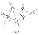
- the network includes an operator or switch such as A, B, C, D, E and F.
- Each operator includes a microcomputer whose volume of information that it can process fixes the power of the operator.
- Each operator also has an interface to the outside connected to a trunk circuit or a subscriber circuit of the telephone network or to the data switching network.
- the interface 1 to the outside is connected to junction a.
- Each operator finally has an inward interface connected at least to another network operator and at most to all other network operators.
- These links or meshes of the network are constituted by channels which comprise the two directions of communication.
- the inward interface 2 is connected to operator B by channel 3, to operator F by channel 4 and to another network operator by channel 5.
- FIG. 2 represents the block diagram of an operator comprising a switching level in accordance with the invention.
- This operator comprises an upper level 6 constituted by a microcomputer 7 and an interface to the outside consisting of a reception part 8 and a transmission part 9.
- the reception part 8 has the function of forming, with the help of the microcomputer, the packets from the information provided by the junction.
- the operator relates more particularly to the switching of digital data by “self-directed” packets, that is to say that each packet has a header which comprises as many selection labels as there are switches as the packet must cross in the network, each selection label being associated with a switch and indicating the identity of the downstream channel to be selected, and in which the selection labels are arranged in the order of the switches that the message must cross. It is the reception part 8 which determines the path to be traversed through the network and which registers the header of each packet.
- the transmission part 9 performs the reverse transformation and transmits the reshaped information on the junction.
- Another function of the upper level 6 is the processing of erroneous packets.
- the operator also includes a switching level 10, which is the subject of the patent, which consists of n bidirectional doors such as door 11.
- a switching level 10 which is the subject of the patent, which consists of n bidirectional doors such as door 11.
- One of these doors (door 11 in FIG. 2) provides the link with the upper level. 6, the others are connected to bidirectional gates of switching levels of other network operators.
- Each bidirectional door such as 11 comprises an entry door or reception circuit 12 and an exit door which comprises a transmission circuit 13 preceded by a storage device 14.
- Each reception circuit has an input and an output as well.
- each transmission circuit and each storage device comprises n storage circuits, each of these n circuits being assigned to one of the n operator reception circuits.
- each reception circuit can be connected to one of the n storage circuits which are allocated to it, the connections all being carried out by means of the same three-state bus line.
- the operator finally includes an internal clock 16.
- FIG. 4 gives an exemplary embodiment of the switching level shown diagrammatically in FIG. 2.
- This type of transmission has the advantage of reducing interface hardware as much as possible.
- a reception circuit 12 has an input in theory, which corresponds to two inputs in practice: one for the data D., one for the clock HD.
- the function of this reception circuit is to transform “serial” data at the rate of the clock received HD into “parallel data at the rate of the local clock HL supplied by the internal clock 16 of the same nominal frequency as the remote clock. .
- This circuit 12 is shown in FIG. 3. It comprises two shift registers 16 and 17 with a serial input and eight outputs in parallel, the serial input of each of these registers 16 and 17 receiving the data D.
- the circuit 12 also includes a counter 18 with four binary elements, the clock input of which receives the HD signal and the output of which is connected on the one hand to one of the inputs of an AND gate 19 via an inverter 21 , on the other hand to one of the inputs of an “AND” gate 20.
- the “AND” gate 19 receives on its other input the clock signal HD and its output is connected to the clock input of the register 16.
- the AND gate 20 receives on its other input the clock signal HD and its output is connected to the clock input of register 17.
- the clock input of register 16 receives the signal HD for eight periods of this signal; this which corresponds to the writing of a byte in the register 16, during this time the clock input of the register 17 receives a constant signal and the content of the register 17 is unchanged. During the following eight periods of the HD signal, the procedure is reversed and a byte is written into register 17.
- the reception circuit 12 comprises four flip-flops 22, 23, 24 and 25 of type D which receive at the clock input the local clock signal HL.
- flip-flop 22 The input of flip-flop 22 is connected to the output of counter 18 and the input of flip-flop 23 is connected to the output of flip-flop 22.
- the output of flip-flop 23 is connected to the control input of a set of eight doors "three states", represented by a single door 26 in FIG. 3, the inputs of which are connected to the outputs of the registers 16.
- flip-flop 24 is connected to the output of counter 18 via an inverter 27 and the input of flip-flop 25 is connected to the output of flip-flop 24.
- the output of flip-flop 25 is connected to the input of control of a set of eight “three-state” doors, represented by a single door 28 in FIG. 3, the inputs of which are connected to the outputs of the register 17 and the outputs of which are connected to the respective outputs of the assembly 26, providing thus DL data in parallel.
- the flip-flops 22 and 23 are reset to zero by the signal from an AND gate 29 which receives as input the read authorization signal from the register 16 from the flip-flop 23 and a signal COMi from the control circuit 15.
- the flip-flops 24 and 25 are reset to zero by the signal from an “AND” gate 30 which receives the input of the read authorization signal from the register 17 from the flip-flop 25 and the signal COMi.
- the reception circuit 12 therefore supplies, without delay and without conflict between clocks, the data DL per byte in parallel and at the rate of the internal clock HL.
- the reception circuit 12 provides a signal EN which indicates that the input is active, when it is at the high logic level, and which comes from a monostable 31 with retriggering which receives as input the HD remote clock signal.
- circuit 12 provides a signal OP which comes from an “AND 32 gate receiving the two read authorization signals from registers 16 and 17 and which indicates, when it is at the high logic level, that a byte is ready to read.
- the data outputs DL of the n reception circuits are all connected to the common bus 33 in three states and all the outputs of the signals EN and OP are connected to the control circuit 15, as shown in FIG. 4.
- the control circuit 15 is common to all the circuits of the switching level; to successively process the data coming from the n reception circuits, it includes a counter 34 "modulo n which supplies a COM signal and which is activated by an oscillator 35.
- the period of the local clock HL being equal to T seconds, each gate d input provides one byte every 8T seconds and the control circuit must therefore read all of the n gates in a cycle of 8T seconds, the oscillator 35 therefore has a period P equal to 8T / n and is synchronous with the local clock HL.
- the activity indication output EN of each of the n reception circuits 12 is connected to one of the n inputs of a multiplexer 37 which outputs an ENO signal; similarly, the byte availability OP indication output of each of the n reception circuits 12 is connected to one of the n inputs of a multiplexer 38 which outputs an OPO signal.
- the two multiplexers 37 and 38 receive the COM signal as a control input so that when the COM signal is equal to i (i taking the values 1 to n) the signals from the multiplexers 37 and 38 are identical to the signals from the i th circuit reception.
- the control circuit 15 comprises a first part dedicated to the cyclic reading of the n reception circuits 12 and to the writing of the n storage devices 14 and to the writing of the n transmission circuits 13.
- Each storage device 14 comprises a random access memory 39 of x words of nine binary elements which is divided into as many pages as there are reception circuits, that is to say n in this example, which has been shown very schematically in Figure 2.
- Each device 14 also includes a memory 40 of the “first in, first out” (FIFO) type associated with the RAM 39 and allowing the marking of priorities.
- Each of the parts of the control circuit consists of programmed logic of n words preceded by programmed read only memories.
- the first part therefore includes a programmed logic 43 of n status words in writing of the storage memories.
- Each of the n words represents the work to be performed on the byte which occurs on the corresponding reception circuit.
- AD bits indicate the address where to write the byte in the page assigned to the gate through which the packet enters the RAM memory of the addressed output gate.
- the last IPS binary elements indicates the identity or address of the door through which the packet must exit, it is the first selection label for the header of the package.
- the control logic 43 receives an ESO signal constituted by binary elements in parallel and coming from an “AND” gate 44 which receives via an “AND” gate 45 the signal OPO, the signal AC inverted by gate 46 and the FA signal inverted by gate 47.
- the ES signal comes from a control circuit 48 which is connected to the common bus 33.
- the ES signal consists of / first binary elements of one byte in parallel, the ESO signal consists of 1 first binary elements of the first byte of a package.
- the circuit 48 supplies an error signal ER to the memory 50, this signal ER is established by the circuit 48 from the 8-I control binary elements (for example by redundancy) which accompany the first 1 binary elements.
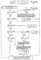
- the logic 43 is addressed by the signal COM and it is preceded by a read-only memory 49, which receives the address AD from 43 and provides it with the new address AD + 1, and by a read-only memory 50 which receives the signals as input.
- OPO is equal to "1"
- AC - FA is the second byte of the packet which must be in output the first byte of the transmitted packet and we test IRO to know on the queue corresponding to the indicated output by IPS is full.
- the second part of the control circuit 15 includes programmed logic 51 of n status words for reading the storage memories.
- the structure of a read status word is that shown in FIG. 6a.
- Each of the n words represents the work to be performed on the corresponding storage memory.
- the first binary element PO indicates when it is "1" that we are going to read the first byte of a packet.
- the second binary element AC indicates when it is at "1" that a reading activity is in progress.
- bits AD 'and COM' respectively indicate the address in the page and the page where to read the byte.
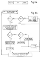
- the logic 51 is addressed by the signal COM and it is preceded by a read only memory 52, which receives the address AD 'from 51 and supplies it with the new address AD' + 1, and by a read only memory 53 which receives as input the signal AC 'coming from 51, the signal ORO coming from 42 and the signal POL which is the last binary element of the words read in the storage memories 39 together with the data and which supplies the logic 51 with the new information PO 'and AC', the control logic 51 directly receiving the addressing information ADO and COMO from the priority memories 40.
- This binary element POL is equal to "1", only when it accompanies the first byte of a packet and when the word read is the end indication word.
- ORO is equal to “1” during the rewriting of the m th status word, we write “1” in the space reserved for AC 'as well as in that reserved for PO' and we write ADO and COMO respectively in the spaces reserved for AD 'and COM'; then go to the next status word.
- the output register 13 is loaded with the data DP and during the rewriting of the status word, we write "0" at the location reserved for PO'; then go to the next status word.
- POL is '0 and PO' is '1', it means that a packet has been overloaded, there has been an overlap; no packet is emitted, the upper level is informed, then the status word is reset and the next status word is passed.
- control circuit 15 comprises an output multiplexer 54 which receives from the first write control part three signals, firstly the signal IPS, secondly the signal COM and thirdly the signal AD and which receives second control part for reading three signals, firstly the COM signal, secondly the COM 'signal and thirdly the AD' signal.
- This multiplexer 54 is controlled by the clock signal from the oscillator 35 which controls the counter 34 so that, the signal COM having the value m for a period, the first half-period is devoted to writing and the second on reading.
- the first output of the multiplexer 54 is connected on the one hand to the control inputs of the multiplexers 41 and 42, on the other hand to the input of a decoder 55 of which each of the n outputs is connected to the input for selecting one of the n devices. storage, that is to say that the i th output of the decoder 55 is connected to the selection inputs of the storage memory 39 and the memory of priority 40 of the i th storage device.
- the assembly constituted by the second and the third output is connected directly to the addressing inputs of each of the storage memories and to the inputs of the priority memories.
- each of the storage memories has its read-write control input connected to the oscillator 35, has eight of its data inputs connected to the common bus 33 and the ninth input being connected to the output of a door “AND” 56 whose inputs receive the signals AC and FA and has eight of its outputs connected to the transmission circuit 13 which corresponds to it; the ninth output being connected to the read-only memory 53 of the control circuit and to the same transmission circuit 13 as the other outputs.
- Each transmission circuit 13, shown in FIG. 7, comprises an output register 57 with eight parallel inputs and one serial output.
- the eight parallel inputs are connected to the eight data outputs of the corresponding storage memory 39, from which they receive the DP data and the output provides the output DS signal, the register clock input receives the HL signal. operator's local clock.
- an “AND 58” gate is used which receives on the one hand the clock signal HL, on the other share a signal V of validation and which provides the signal HS.
- the validation signal V comes from a flip-flop 59 of RS type, the input S of which is connected to the output of an “AND” gate 60 which receives the signal PO 'coming from the logic 51 of the control circuit and the signal POL from the storage memory at the same time as the data DP and the input R of which is connected to the output of an “AND” gate 61 which receives the signal POL and the signal PO 'inverted by the inverter 62 .
- the operator which has a switching level similar to that described in this patent, is able to connect any input to any output, so there is total accessibility and in a simple way thanks to the omnibus line common.
- the queues at the exit gates are filled only with useful information, a single POL binary element making it possible to obtain the start and end of packet information; the use of random access memories for these queues is very economical.
- control detects an erroneous packet, it is not taken into account and the upper level is informed.
Landscapes
- Engineering & Computer Science (AREA)
- Computer Networks & Wireless Communication (AREA)
- Signal Processing (AREA)
- Data Exchanges In Wide-Area Networks (AREA)
Applications Claiming Priority (2)
| Application Number | Priority Date | Filing Date | Title |
|---|---|---|---|
| FR7914124 | 1979-06-01 | ||
| FR7914124A FR2458196A1 (fr) | 1979-06-01 | 1979-06-01 | Niveau de commutation d'un operateur pour reseau de commutation de donnees numeriques par paquets |
Publications (2)
| Publication Number | Publication Date |
|---|---|
| EP0020255A1 EP0020255A1 (fr) | 1980-12-10 |
| EP0020255B1 true EP0020255B1 (fr) | 1983-03-09 |
Family
ID=9226155
Family Applications (1)
| Application Number | Title | Priority Date | Filing Date |
|---|---|---|---|
| EP19800400728 Expired EP0020255B1 (fr) | 1979-06-01 | 1980-05-23 | Niveau de commutation d'un opérateur pour réseau de commutation de données numériques par paquets |
Country Status (6)
| Country | Link |
|---|---|
| EP (1) | EP0020255B1 (ref) |
| BR (1) | BR8003371A (ref) |
| DE (1) | DE3062265D1 (ref) |
| ES (1) | ES491995A0 (ref) |
| FR (1) | FR2458196A1 (ref) |
| GR (1) | GR68473B (ref) |
Cited By (1)
| Publication number | Priority date | Publication date | Assignee | Title |
|---|---|---|---|---|
| US4623996A (en) | 1984-10-18 | 1986-11-18 | Mcmillen Robert J | Packet switched multiple queue NXM switch node and processing method |
Families Citing this family (11)
| Publication number | Priority date | Publication date | Assignee | Title |
|---|---|---|---|---|
| EP0073078B1 (en) * | 1981-08-21 | 1986-10-29 | ITALTEL SOCIETA ITALIANA TELECOMUNICAZIONI s.p.a. | Modular switching network for telecommunication system |
| FR2539939B1 (fr) * | 1983-01-21 | 1989-03-24 | Thomson Csf Mat Tel | Unite de commutation pour commutateur de donnees numeriques par paquets |
| FR2549673B1 (fr) * | 1983-07-19 | 1989-06-30 | Thomson Csf Mat Tel | Commutateur elementaire pour autocommutateur utilisant une technique de multiplexage asynchrone |
| US4630258A (en) * | 1984-10-18 | 1986-12-16 | Hughes Aircraft Company | Packet switched multiport memory NXM switch node and processing method |
| US4837676A (en) * | 1984-11-05 | 1989-06-06 | Hughes Aircraft Company | MIMD instruction flow computer architecture |
| US4780870A (en) * | 1986-09-05 | 1988-10-25 | American Telephone And Telegraph Company, At&T Bell Laboratories | Packet switch |
| BE1000396A7 (fr) * | 1987-03-18 | 1988-11-22 | Electronique Et Telecomm Bell | Systeme de commutation. |
| WO1990004316A1 (en) * | 1988-10-03 | 1990-04-19 | Alcatel N.V. | Communication switching element |
| EP0492026B1 (en) * | 1990-12-20 | 1995-07-26 | International Business Machines Corporation | Modular buffer memory for packet switched network |
| US6920510B2 (en) * | 2002-06-05 | 2005-07-19 | Lsi Logic Corporation | Time sharing a single port memory among a plurality of ports |
| CN113923722B (zh) * | 2021-10-11 | 2023-06-13 | 中国联合网络通信集团有限公司 | 数据传输方法、装置及存储介质 |
Family Cites Families (1)
| Publication number | Priority date | Publication date | Assignee | Title |
|---|---|---|---|---|
| CH591190A5 (ref) * | 1975-04-25 | 1977-09-15 | Hasler Ag |
-
1979
- 1979-06-01 FR FR7914124A patent/FR2458196A1/fr active Granted
-
1980
- 1980-05-23 DE DE8080400728T patent/DE3062265D1/de not_active Expired
- 1980-05-23 EP EP19800400728 patent/EP0020255B1/fr not_active Expired
- 1980-05-28 GR GR62062A patent/GR68473B/el unknown
- 1980-05-29 BR BR8003371A patent/BR8003371A/pt unknown
- 1980-05-30 ES ES491995A patent/ES491995A0/es active Granted
Cited By (1)
| Publication number | Priority date | Publication date | Assignee | Title |
|---|---|---|---|---|
| US4623996A (en) | 1984-10-18 | 1986-11-18 | Mcmillen Robert J | Packet switched multiple queue NXM switch node and processing method |
Also Published As
| Publication number | Publication date |
|---|---|
| DE3062265D1 (en) | 1983-04-14 |
| BR8003371A (pt) | 1980-12-30 |
| FR2458196A1 (fr) | 1980-12-26 |
| GR68473B (ref) | 1982-01-04 |
| EP0020255A1 (fr) | 1980-12-10 |
| FR2458196B1 (ref) | 1982-01-15 |
| ES8102448A1 (es) | 1980-12-16 |
| ES491995A0 (es) | 1980-12-16 |
Similar Documents
| Publication | Publication Date | Title |
|---|---|---|
| EP0293315B1 (fr) | Système et méthode de contrôle de flux de paquets | |
| EP0003493B1 (fr) | Système de transmission de données entre des stations connectées en boucle | |
| EP0020255B1 (fr) | Niveau de commutation d'un opérateur pour réseau de commutation de données numériques par paquets | |
| FR2480460A1 (fr) | Dispositif pour transferer des informations entre des unites principales d'un systeme de traitement de donnees et un sous-systeme central | |
| EP0113639A1 (fr) | Système de commutation de paquets synchrones de longueur fixe | |
| FR2480458A1 (fr) | Dispositif pour transferer des informations entre des unites d'un systeme de traitement de donnees | |
| EP0094322B1 (fr) | Coupleur à haut débit entre un multiplex de voies MIC et un commutateur de paquets | |
| EP0041001B1 (fr) | Perfectionnements aux réseaux de commutation numérique à division du temps bit à bit | |
| FR2519441A1 (fr) | Systeme de selection de priorite pour l'acces a un bus utilise en mode partage | |
| EP0120495B1 (fr) | Dispositif d'échange de messages codés entre stations | |
| EP0026708A1 (fr) | Système de diffusion de données et équipement de réception utilisé dans un tel système | |
| EP0383660B1 (fr) | Réservation de débits dans un réseau de paquets asynchrones | |
| BE897587A (fr) | Circuit parallele de controle de redondance cyclique | |
| EP0920157A1 (fr) | Dispositif de gestion de mémoire tampon partagée | |
| EP0340841A1 (fr) | Elément de circuit-point de croisement entre deux lignes omnibus | |
| EP0035926B1 (fr) | Système de commutation de signalisation dans un réseau de commutation temporelle, et réseau de commutation temporelle comportant un tel système | |
| EP0018618B1 (fr) | Dispositif de synchronisation de multiplex dans un central de commutation temporelle | |
| EP0166837B1 (fr) | Dispositif de rebouclage pour un système de communication de données sur une liaison multiplex | |
| CA1092225A (fr) | Central telephonique et les circuits de commande associes | |
| EP0052863B1 (fr) | Dispositif d'adressage d'un ensemble d'enregistreurs d'un central de commutation | |
| EP0301934B1 (fr) | Système de commutation temporel de paquets de différentes longueurs | |
| EP0298793B1 (fr) | Circuit pour mémoriser des états de disponibilité de ressources logiques, telles que cellules de mémoire, et établir des adresses de ressources libres | |
| FR2520956A1 (fr) | Systeme de transmission asynchrone, notamment pour systeme de videotex interactif | |
| EP0689319A1 (fr) | Dispositif d'acheminement de cellules de données ATM | |
| FR2465377A1 (fr) | Interface de passage a une liaison de transmission en mode " paquets " a partir d'une liaison de transmission numerique d'un autre mode |
Legal Events
| Date | Code | Title | Description |
|---|---|---|---|
| PUAI | Public reference made under article 153(3) epc to a published international application that has entered the european phase |
Free format text: ORIGINAL CODE: 0009012 |
|
| AK | Designated contracting states |
Designated state(s): BE DE GB IT NL |
|
| 17P | Request for examination filed |
Effective date: 19810115 |
|
| GRAA | (expected) grant |
Free format text: ORIGINAL CODE: 0009210 |
|
| AK | Designated contracting states |
Designated state(s): BE DE |
|
| REF | Corresponds to: |
Ref document number: 3062265 Country of ref document: DE Date of ref document: 19830414 |
|
| PGFP | Annual fee paid to national office [announced via postgrant information from national office to epo] |
Ref country code: BE Payment date: 19910605 Year of fee payment: 12 |
|
| PG25 | Lapsed in a contracting state [announced via postgrant information from national office to epo] |
Ref country code: BE Effective date: 19920531 |
|
| BERE | Be: lapsed |
Owner name: THOMSON-CSF TELEPHONE Effective date: 19920531 |
|
| PGFP | Annual fee paid to national office [announced via postgrant information from national office to epo] |
Ref country code: DE Payment date: 19970510 Year of fee payment: 18 |
|
| PG25 | Lapsed in a contracting state [announced via postgrant information from national office to epo] |
Ref country code: DE Free format text: LAPSE BECAUSE OF NON-PAYMENT OF DUE FEES Effective date: 19990302 |
|
| PLBE | No opposition filed within time limit |
Free format text: ORIGINAL CODE: 0009261 |
|
| STAA | Information on the status of an ep patent application or granted ep patent |
Free format text: STATUS: NO OPPOSITION FILED WITHIN TIME LIMIT |