EP0018869B1 - Installation de cryptage et de décryptage d'un signal analogique par compressions et expansions temporelles - Google Patents
Installation de cryptage et de décryptage d'un signal analogique par compressions et expansions temporelles Download PDFInfo
- Publication number
- EP0018869B1 EP0018869B1 EP80400476A EP80400476A EP0018869B1 EP 0018869 B1 EP0018869 B1 EP 0018869B1 EP 80400476 A EP80400476 A EP 80400476A EP 80400476 A EP80400476 A EP 80400476A EP 0018869 B1 EP0018869 B1 EP 0018869B1
- Authority
- EP
- European Patent Office
- Prior art keywords
- signal
- analog
- period
- pulses
- during
- Prior art date
- Legal status (The legal status is an assumption and is not a legal conclusion. Google has not performed a legal analysis and makes no representation as to the accuracy of the status listed.)
- Expired
Links
Images


Classifications
-
- H—ELECTRICITY
- H04—ELECTRIC COMMUNICATION TECHNIQUE
- H04K—SECRET COMMUNICATION; JAMMING OF COMMUNICATION
- H04K1/00—Secret communication
- H04K1/06—Secret communication by transmitting the information or elements thereof at unnatural speeds or in jumbled order or backwards
Definitions
- the present invention relates to an encryption and decryption installation comprising an encryptor for encrypting an initial analog incoming signal into an analog encrypted signal and a decryptor for decrypting the analog encrypted signal into an analog decrypted signal analogous to said initial analog signal and as defined in the preamble of claim 1.
- the invention applies in particular to the encryption and decryption of an audio frequency signal from a radio broadcast or, more generally, to the coding and decoding, encryption and decryption, or to the scrambling and unscrambling of an analog signal.
- Encryption and decryption installations using a sampling of the analog signal at predetermined periodic times and then arranging or scrambling these samples are already known in the prior art. All the arithmetic coding methods can be applied, the simplest consisting of coding according to a pseudo-random sequence one according to permutation sequences of one or more samples.
- the delay means of the encryptor, resp. of the decryptor are constituted by two true analog memories, although called “analog shift registers" each composed of N sample cells individually addressable for writing and reading.
- the inputs of the memories receive alternately, for a period NT e out of two of the encryption signal, resp. decryption, N samples in series of the initial incoming signal, resp. crypt.
- the 2N outputs of the cells of the two analog memories are connected in parallel to the output of the encryptor, resp. of the decryptor, through an analog switching circuit.
- the analog switching circuit acts as a parallel to serial converter.
- the encryption signal resp. decryption, in order to select alternately in reading, for two consecutive NT periods .
- the N outputs of one of the memories then the N outputs of the other memory.
- the N cells of a memory are read in a predetermined order, so as to read the previously written samples in a different order. This amounts to performing a permutation, at the same reading frequency as that of writing 1 / T 8 .
- the encryption signal thus reads the N cells of a memory according to a predetermined permutation and at a constant reading frequency.
- the decryption signal In the decryptor, to reconstitute the initial analog signal, the decryption signal must consist of a series of address words according to the permutation complementary to that of encryption.
- the means for producing the encryption signal in the encryptor and the means for producing the decryption signal are necessarily different.
- the fact that it is necessary to address the outputs of the memories in a predetermined order different from the initial order of writing and sampling of the initial signal considerably complicates the logic of the installation.
- Such provisions confer a relatively high cost of installation, which limits the number of listeners likely to acquire a decryptor for specialized programs, these listeners are not, a priori, experienced professionals.
- the delay line enchants the incoming signal and transfers from the input to the output by successive writing and reading in its different analog stages in series the samples under the control of complementary logic signals emanating from the same modulation signal. There is then temporal expansion and compression of the samples.
- the initial sampling is not regular, that is to say is not rhythmic at constant period, and if the initial incoming signal varies significantly when the imposed delay is large, that is say when the difference between two successive sampling instants is large, the signal decrypted on reception may be correspondingly different.
- This installation also has the following second drawback.
- the writing and reading in the delay line being punctuated by the same encryption signal in the encryptor, it is then necessary to compensate for the delays in the decryptor by delaying the encrypted signal according to. reverse order of delays in the encryptor.
- the decryption signal is the reverse of the encryption signal, this condition having the disadvantages already mentioned for US-A-4,100,374.
- the object of the present invention is to provide an installation for encryption and decryption of the type defined in the introduction which is freed from the above drawbacks by the fact that the analog samples of the initial signal have their order preserved in the analog signal. encrypted and undergo without loss of sample at least one time compression for each period of the encryption signal, which is also used as a decryption signal.
- the distribution of the analog samples in the encrypted signal fluctuates in a manner analogous to a weeping effect without the initial order of the samples being changed.
- the time delay or compensation and expansion function of the initial or encrypted signal is carried out by means of two delay lines comprising analog shift registers such as charge transfer circuits, known by the American acronym C.T.D. ("charge tranfer device").
- analog shift registers such as charge transfer circuits, known by the American acronym C.T.D. ("charge tranfer device").
- a first combination of the two delay lines in the encryptor, resp. in the decryptor is determined in claim 2.
- Each period NT e corresponds to the duration of filling of all is stages of a delay line during which are written in the encryptor, resp. are read in the decryptor the N samples of the initial signal, res. decrypted.
- one of the two delay lines is commanded to write to the encryptor at the rate of the period of the writing clock pulses, resp.
- a second combination of the two delay lines in the encryptor, resp. the decryptor is determined in claim 3.
- the means for synchronously producing the identical encryption and decryption signals are generally based on the pulse modulation of a predetermined signal. This modulation can be of the position or frequency type and the frequency of the modulation signal can also be programmable. According to another less complex variant, the means for producing the encryption or decryption signal are programmable frequency multipliers or dividers. The selection of these different means and the programmable frequency makes it possible to generate a plurality of codes, each of which is assigned to a specialized program.
- the pulse modulation produces a number of pulses greater than the number of analog samples during a period of the encryption and decryption signal
- a counter counts the first N pulses of the code signal at the start of each period and blocks the transmissions of the following pulses until the start of the next period.
- N samples of the encrypted signal are always time compressed for a period NT ,,.
- the time interval between two successive samples of the same period NT e can be greater than T 8 .
- the samples of the signal encrypted in a period NT e can be followed by a more or less long silence interval.
- the encrypted signal is suitable for being conveyed by a transmission channel between the encryptor and the decryptor which can be of the type by cables, by hertzian way, by optical fibers, by direct diffusion, such as by the intermediary of a satellite, or by any other type of diffusion, and the decrypted signal always presents characteristics of correct quality of listening.
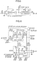
- the encryption and decryption installation in accordance with the invention comprises, on transmission, an encryptor 1 and on reception, a decryptor 2.
- the output of the encryptor 1 is connected to the input of the decryptor 2 through a transmission 3.
- the input of encryptor 1 receives the initial analog signal to be encrypted.
- This signal is a speech signal and / or a musical signal, and is transmitted by a tape recorder or the audio tape of a VCR of the recording chain of a studio of a radio or television station for example.
- a low-pass filter 10 filters the initial analog signal in a low frequency band which extends up to 8 kHz, for example.
- the filtered signal is optionally transmitted to a pre-emphasis and / or compression circuit 11, the output of which is connected to the input 120 of an analog delay circuit 12.
- the circuit 11 contributes to improving the performance of the encryptor by masking the faults possible due to sampling and switching inherent in encryption.
- the signal / noise ratio is also increased thanks to circuit 11.
- the delay circuit 12 consists of two analog delay lines 121 ,, 121 2 which are connected in parallel, and by an analog switching circuit 122.
- the common inputs 120 of the delay lines 121 ,, 121 are connected to the output of the pre-emphasis and / or compression circuit 11.
- the outputs of the last stages of the delay lines 121 1 , 121 2 are respectively connected to the two analog inputs of two analog AND gates 123 1 and 123 2 which are included in circuit 122.
- This duration NT e is equal to the period of the encryption and decryption code signals.
- the outputs of analog AND gates 123, and 123 2 are connected to the inputs of an analog OR gate 124 whose output 125 transmits the encrypted signal.
- each analog delay line is an integrated charge transfer circuit or is composed of several integrated charge transfer circuits connected in series. Although reference is made in the following to such a series connection, the charge transfer circuits of a delay line can be connected in parallel or in series-parallel.
- CTD charge transfer device
- BBD boostet brigade device
- each analog delay line 121 1 , 121 2 includes P analog shift registers. Each register consists of 512 serial stages of the BBD type.
- the delay provided by a 512-stage register is equal to 512 ⁇ 0.05 / 2 ms.
- the complementary read (or write) control signals S 1 and S 2 transmitted by the addressing circuit 13 to the gates 123 2 and 123 1 have a period equal to 2 NT .
- the pulse signals transmitted on the output wires 126, and 126 2 by the addressing circuit control the step-by-step advance of a sample in the delay lines in the reading phase and have equal a period equal to 2 NT e .
- One of them, such as the one on wire 126 1 is composed during a first half-period NT e by N pulses at the constant period T e which control the sampling and writing in the delay line 121 1 .
- the second half-period following NT e is composed by N pulses which control the reading of the N samples written in the delay line 121 1 and which are not evenly distributed in time.
- the read pulses have a time distribution determined by the encryption code and different from that regular of the previous write pulses.
- the other impulse signal on wire 126 2 is composed during the first preceding half-period NT e by N pulses which have said determined time distribution and which control the reading of N samples in the delay line 121 2 , and is composed during the second preceding half-period NT e by N pulses which are equidistributed in the constant period T e and which control the writing of N samples in the delay line 121 2 .
- the second delay line 121 2 is in the read phase for which the samples of the initial input signal, previously delayed advance at successive instants t 1 to t N distributed according to the encryption code during the same half-period NT B.
- the previous read and write phases are reversed: the first delay line 1211 is in the read phase and the second delay line 122 2 is in the write phase.
- the successive reading instants t 1 to t N are produced according to an encryption code selected by a control unit 15 possibly dependent on the clock signal at the frequency F e on the wire 140.
- the unit 15 transmits via the bus 150 the pulses at instants t 1 to t N during each duration NT e to the addressing circuit 13.
- a synchronization unit 16 receives on two output wires 160 of the addressing circuit 13 the complementary read and write control signals S 1 and S 2 to produce synchronization pulses at the frequency NT e which make it possible to reconstitute the initial signal suitably from the signal encrypted in the decryptor 2.
- the synchronization pulses are transmitted on wire 161 to the control unit 15 and are suitably modulated, by a signal at a high frequency transmitted through the output wire 141 by the clock 14, into a synchronization signal on the output 162 of the circuit 16.
- the encrypted signal and the synchronization signal are mixed in a mixer 17 after respective passage through a low-pass filter 171 which is analogous to filter 10, and a band-pass filter 172 whose bandwidth is centered on the modulation frequency synchronization.
- the composite signal from the output of the mixer 17 is possibly transmitted and suitably shaped in a transmission modulator 18 depending on the mode of transmission of the channel 3 between the encryptor 1 and the decryptor 2.
- the composite signal On reception in the decryptor 2, the composite signal optionally passes through a suitable reception demodulator 28, then is filtered.
- a low pass filter 271 which is analogous to filter 10
- a bandpass filter 272 which is analogous to filter 172, output the encrypted signal and the synchronization signal, respectively.
- the decryptor 2 performs the opposite function to that of the encryptor and comprises, in a manner similar to the circuits 12 to 16 of the encryptor, circuits 22 to 26.
- An analog delay circuit 22 receives by its input 220 the encrypted signal transmitted by the low-pass filter 271, and restores by its output 225 the decrypted signal which is analogous to that received at the input 120 of the analog delay circuit 12 of the encryptor 1.
- a write and read addressing circuit 23 controls alternately in writing and reads the two analog delay lines 221 1 and 221 2 of the circuit 22, via the wires 226 1 and 226 2 .
- the addressing circuit 23 controls, through the wires 227 1 and 227 2 , alternately during the readings, the analog AND gate openings 223 1 and 223 2 of the analog switching circuit 222 which is included in the circuit 22.
- the circuit 222 is identical to the circuit 122 and also includes an analog OR gate 224 whose output 225 transmits the decrypted signal.
- a clock 24 transmits a clock signal at the constant frequency F e on the wire 240 to the addressing circuit 23 and a control unit 25.
- This unit 25 has previously recorded the decryption code which is, in accordance with invention, identical to the selected encryption code and transmits on the wire 250 the writing pulses at variable times t 1 to t N to the addressing circuit 23.
- the synchronization pulses are detected in a synchronization circuit 26 from the synchronization signal transmitted by the filter 272 and are transmitted over the wire 261 to the control unit 25 and the clock 24.
- the synchronization signal also makes it possible to control the advance of the recording medium at the listener, such as as the recording tape of a tape recorder for example (not shown).
- the analog decrypted signal analogous to the initial analog signal which is received by the input 120 of the delay circuit 12 in the encryptor is transmitted by the output 225 of the analog switching circuit 222 to a low-pass filter 20 which is analogous to the filter 10, then optionally to a de-emphasis and / or extension circuit 21 which is completed signal from circuit 11.
- the output of circuit 21 common to that of decryptor 2 restores a decrypted analog signal which is analogous to the initial analog signal received at the input of the encryptor.
- the control unit 15 produces the N pulses the reading at times t 1 to t H such that, in general, t i + 1 -t i ⁇ T e with 1 ⁇ i ⁇ N.
- the distribution of the N read pulses in a read interval NT e is obtained by means of a so-called pulse modulation circuit 151.
- This circuit 151 may include one or more "pulse modulators” or “read clocks with not variable "1510 which are programmable or not and which each generate a sequence of read pulses having a duration NT B.
- a modulator 1510 is a programmable frequency multiplier which multiplies by a predetermined integer Q a reference frequency, for example the frequency F e transmitted by the clock 14 on the wire 140.
- a modulator 1510 is a "pulse modulator" of a periodic or non-periodic signal, preferably with a single envelope. This signal can be a periodic sawtooth signal as shown in line b of FIG. 2 or a periodic signal at several levels as shown in line c of FIG. 2. Such a signal is produced by a signal generator included in the modulator 1510.
- the modulation circuit included in the modulator 1510 operates according to one of the known pulse modulations. If the modulation is a position modulation, that is to say if the time positions of the pulses are proportional to the amplitude of the modulating signal, the read pulses are distributed as shown in lines b 1 and c, of FIG . 2. When the modulation is a frequency modulation, sequences of pulses at predetermined frequencies correspond to the predetermined levels of the modulating signal, as shown in lines b 2 and c 2 of FIG. 2. It will be noted that other "pulse modulations" 1510 can be easily imagined for those skilled in the art and can result from the combination of the preceding variants.
- modulators of the sawtooth or multilevel type may have the frequency of the programmable modulation signal.
- the encryptor and especially the decryptor will include one or more "pulse modulators" which allow each to generate an encrypted signal which is, to a large extent, practically incomprehensible.
- the pulse modulators and / or the frequencies of the modulating signal thereof are addressed by a read-only memory of encryption codes 152 of the control unit 15 shown in FIG. 4.
- Each cell 1520 of the memory 152 contains the address of a modulator 1510 and, if necessary, of one of the modulation frequencies.
- This code memory 152 is addressed, in a known manner, for reading by an alphanumeric keyboard 153 through a code address register 154 which corresponds to each number identifying an encryption code and transmitted by the keyboard 153, l address of a cell 1520 of the memory 152.
- the pulse modulator 1510 addressed is powered up and produces on the output 1511 of the circuit 151 through an OR gate 1512 the read pulses at predetermined times t, at t N.
- the control unit 15 comprises a counter 155 with a maximum count N whose counting input is connected to the output 1511 of the modulation circuit 151, and an AND gate 156 having its inputs connected to the output 1550 of the counter 155 and at terminal 1511.
- Counter 155 is reset to zero (RESET) each time it receives a synchronization pulse which is transmitted on wire 161 by synchronization circuit 16 and which defines a transition between the phases of reading and writing of duration NT e relative to each delay line.
- the counter 155 delivers on its output 1550 a signal which closes the AND gate 156 until the next reset, so that N read pulses only pass through the AND gate 156 pen for a period of NT e .
- the N transmitted read pulses are shown in solid lines on lines a, b 1 , b 2 , c 1 and c 2 in FIG. 2, while the following pulses, which are inhibited, are shown in dotted lines.
- the synchronization pulse on wire 161 is also transmitted to the selected modulator 1510 so that it is reset at the start of each reading and writing phase of duration NT, to produce a modulation signal of period NT e , as shown in lines b and c of FIG. 2.
- the addressing circuit 13 shown in FIG. 3 produces the signal S, which simultaneously controls the writing phase of the delay line 121, and the reading phase of the delay line 121 2 .
- the addressing circuit 13 also produces the signal S 2 which controls the read phase of the delay line 121, and the write phase of the delay line 121 2 .
- the signal S 1 is produced at the output of a frequency divider by N 130 whose input receives the write pulses at the constant frequency F e which are transmitted by the clock 14 on the wire 140.
- the addressing circuit 13 also comprises two identical logic circuits allowing the alternating transmission of the writing pulses and of the reading pulses to the delay lines 121 1 , 121 2 .
- Each logic circuit is constituted by a first AND gate 132 1 , 132 2 which controls the writing in the delay line 121 1 , 121 21 by a second AND gate 133 1 , 133 2 which controls the reading in the delay line 121 1 , 121 2 and by an OR gate 134 1 , 134 2 whose inputs are connected to the outputs of the first and second doors AND 132 1 , 133 ,, resp.
- Two common inputs of the AND gates 132 1 and 133 2 receive the signal S, which also controls the opening of the analog AND gate 123 2 of the control circuit 122 via the wire 127 2 .
- Two common inputs of the AND gates 133 1 and 132 2 receive the signal S 2 which also controls the opening of the analog AND gate 123, of the switching circuit 122 via the wire 127,.
- the other inputs of the so-called write gates 132 and 132 2 receive, through the clock output wire 140, the write pulses at the constant frequency F e and control alternately during the successive durations NT e the sampling and writing the initial signal in the delay lines 121, and 121 2 .
- the other inputs of the so-called read doors 133 and 133 2 receive, through the output wire 150 of the control unit 15, the read pulses and control, alternately, during the successive durations NT e the reading and the transmission of the encrypted signal from the delay lines 121, and 121 2 , through the analog AND gates 123, and 123 2 which are opened alternately and in correspondence with the openings of the AND gates 133 1 and 133 2 .
- the synchronization circuit 16 is shown diagrammatically in FIG. 5. It comprises a double monostable flip-flop 163 which transmits on the wire 161 a synchronization pulse to each rising edge of the complementary signals S, and S 2 , that is to say at the start of each duration NT . .
- the inputs of the flip-flop 163 are connected to the outputs of the divider 130 and the inverter 131, via the two-wire bus 160.
- the synchronization circuit 16 also includes a frequency modulator 164 whose input is connected at the output of the flip-flop 163 and the output of which transmits the synchronization signal on the wire 162 to the input of the bandpass filter 172.
- the modulator 164 modulates for example in phase the synchronization pulse at a subcarrier frequency of 15 kHz transmitted by the output wire 141 of the clock 14. As already said, this modulated synchronization pulse is mixed with the signal encrypted in the mixer 17 of the encryptor 1 and is detected by the synchronization circuit 26 of the decryptor 2.
- Figs. 3 and 4 it can be seen that the addressing circuits 13, 23 and the control units 15, 25 respectively in the encryptor 1 and the decryptor 2 have respectively identical block diagrams.
- the reference numbers indicated in parentheses correspond to the blocks and wires of the decryptor 2 shown in FIG. 1.
- the synchronization circuit 26 of the decryptor 2 essentially consists of a frequency demodulator whose output 261 transmits the synchronization pulses to the reset input (RESET) of the counter 155 and possibly to the reset input of certain "pulse modulators" 1510 of the control unit 25.
- the synchronization pulses are also received in the clock 24 in order to call the phase servo loop it contains at the frequency F e .
- the listener When the listener wishes to record the program corresponding to the selected encryption code, he types the same identification number on the keyboard 153 of the decryptor 2, which causes, through the register 154 and the code memory 152 of the decryptor, addressing and switching on the corresponding modulator 1510 and, if the latter is programmable in frequency, selecting a frequency of the modulation signal.
- the modulator selected 1510 in the decryptor is identical to that selected in the encryptor. Indeed, the decryptor must recognize after each start of a write interval NT e the samples transmitted by the encryptor to successive reading instants t 1 to t N.
- the writes of the encrypted signal in the two analog delay lines 221 1 and 221 2 during successive intervals of duration NT e must be identical to the reading of the samples in the delay lines 121 1 and 121 2 of the encryptor.
- Reading in the decryptor is identical to writing in the encryptor and is paced at the constant frequency F e . As seen in Fig.
- the so-called write AND gates, 132 1 and 132 2 receive the write pulses with variable distribution according to the encryption code which are transmitted by the output 250 from the control unit 25, while the AND gates called read, 133, and 133 2 , receive the read pulses at constant frequency F e which are transmitted by the output 240 of the clock 24.
- the synchronization circuit 26 synchronizes through the wire 261 the emissions of the write pulses transmitted by the selected modulator 1510 and of the read pulses transmitted by the clock 24, the cutting of the encrypted signal and the reconstitution of the initial signal in the decryptor are controlled in synchronism with the sampling and the reading of the initial signal in the encryptor.
- the two analog delay lines 121 ' 1 , 121' 2 , resp. 222 ' 1 , 221' 2 of the delay circuit 12 ', resp. 22 'in encryptor 1, resp. the decryptor 2 are intended respectively for writing and reading.
- the reference numbers in parentheses represent the components included in the delay circuit 22 'and the write and read addressing circuit 23' of the decryptor which are identical to those 12 'and 13' of the encryptor. Reference is made below to the encryptor, unless otherwise indicated.
- the input 120 ′ of the first stage of the first delay line 121 ′ 1 continuously receives the initial analog signal.
- This delay line samples during each period NT e the initial signal in N serial analog samples at the rate of the periodic writing signal at the constant frequency F e which is transmitted on the wire 126 ' 1 by the addressing circuit 13'.
- the latter opens N analog AND doors 122; at 122 ' N , (resp. 222' 1 to 222 ' N for the decryptor) during the transmission of a synchronization pulse on wire 161 (resp. 261 for the decryptor).
- the other entrances to doors 122; at 122 ′ N are connected to the outputs of the N pairs of stages of the first delay line 121; and simultaneously transmit in parallel the N samples previously stored to the inputs of the N pairs of stages of the second delay line 1212.
- the delay line 121 ′ 2 is read-controlled at times t 1 at t N according to the predetermined distribution of the code selected by the addressing circuit 13 ', via the wire 126' 2 .
- the output 126 ′ of the last stage of the delay line 121 ′ 2 thus delivers the encrypted signal as according to the first embodiment.
- the addressing circuit 13 ′ of the encryptor is much simpler. It now only comprises the frequency divider 130 transmitting the signal S 1 , the inverter 131 transmitting the signal S 2 and two AND gates such as 132 1 and 133 ,. All these components are interconnected in a manner analogous to that shown in FIG. 3.
- the recurrent code sequences of duration NT e are chosen on the one hand, to obtain a completely indecipherable encrypted signal and, on the other hand, to reconstruct the initial analog signal from the encrypted signal with a high signal-to-noise ratio so that the listening quality of the decrypted signal is close to that of the initial signal.
- the choice between the different organizations of the two delay lines and also between the types of pulse modulators depends on operational constraints such as the cost of manufacturing the decryptor, which unlike the encryptor, is made in a large number of 'copies.
- At least one of the control units, 15 and 25, preferably that of the decryptor, can only comprise a single pulse modulator or more simply a multiplier or a frequency divider synchronized with a clock frequency.
- This latter circuit generates a single temporal distribution of the instants t 1 to t N for a duration NT e and can be manufactured in the form of an integrated circuit which is pluggable into the frame of the decryptor. Its power-up is controlled by a simple reset initialization push-button. placing the keyboard. This advantageously makes it possible to effectively control the listening of a predetermined program, since the listener wishing to listen to or record this program will have to obtain such a circuit.
- this selection of listeners can be carried out by decryptors including delay lines with a predetermined number of stages lower than that of the delay lines of the encryptor, which allows for a predetermined transmission to be received by decryptors having delay lines whose number of stages is equal to that actually used in the delay lines of the encryptor. Indeed, it is easy to select in the encryptor of the first stages of a delay line.
- the transmission of the composite signal resulting from the mixture of the encrypted signal and the synchronization signal in the encryptor can be carried out, as already said, by cable, by hertzian way or by optical fiber or the like.
- the initial analog signal can belong to the field of broadcasting, television, telephone, etc.
- the synchronization signal can be mixed with the signal encrypted in this channel, or modulate an audible frequency subcarrier wave, which is mixed with the encrypted signal, the subcarrier being modulated for example in phase by the synchronization signal.
- the composite signal can be transmitted in a conventional television channel, or be temporally multiplexed with the video signal for example by inserting it suitably in line synchronization and blanking signals and / or in frame synchronization and blanking signals.
- any combination of encryption means according to the invention and of decryption means with a view to obtaining an encrypted signal by compression and temporal expansion of an analog signal sampled at constant period or of an analog signal sampled whose samples have been premixed periodically by permutation or in any suitable sequence also falls within the scope of the present invention.
- the reverse operation performed by the corresponding decryptor also belongs to the field of the present invention.
Landscapes
- Engineering & Computer Science (AREA)
- Computer Networks & Wireless Communication (AREA)
- Signal Processing (AREA)
- Two-Way Televisions, Distribution Of Moving Picture Or The Like (AREA)
- Mobile Radio Communication Systems (AREA)
- Signal Processing For Digital Recording And Reproducing (AREA)
Applications Claiming Priority (2)
| Application Number | Priority Date | Filing Date | Title |
|---|---|---|---|
| FR7910092A FR2454664A1 (fr) | 1979-04-20 | 1979-04-20 | Systeme de cryptage et de decryptage d'un signal analogique par compressions et expansions temporelles |
| FR7910092 | 1979-04-20 |
Publications (2)
| Publication Number | Publication Date |
|---|---|
| EP0018869A1 EP0018869A1 (fr) | 1980-11-12 |
| EP0018869B1 true EP0018869B1 (fr) | 1983-05-18 |
Family
ID=9224562
Family Applications (1)
| Application Number | Title | Priority Date | Filing Date |
|---|---|---|---|
| EP80400476A Expired EP0018869B1 (fr) | 1979-04-20 | 1980-04-09 | Installation de cryptage et de décryptage d'un signal analogique par compressions et expansions temporelles |
Country Status (5)
| Country | Link |
|---|---|
| US (1) | US4302628A (ref) |
| EP (1) | EP0018869B1 (ref) |
| CA (1) | CA1142637A (ref) |
| DE (1) | DE3063260D1 (ref) |
| FR (1) | FR2454664A1 (ref) |
Families Citing this family (12)
| Publication number | Priority date | Publication date | Assignee | Title |
|---|---|---|---|---|
| US4392021A (en) * | 1980-07-28 | 1983-07-05 | Technical Communications Corporation | Secure facsimile transmission system using time-delay modulation |
| US4434323A (en) | 1981-06-29 | 1984-02-28 | Motorola, Inc. | Scrambler key code synchronizer |
| US4965825A (en) | 1981-11-03 | 1990-10-23 | The Personalized Mass Media Corporation | Signal processing apparatus and methods |
| EP0117276B1 (en) * | 1982-09-20 | 1990-05-09 | Sanyo Electric Co., Ltd. | Privacy communication apparatus |
| GB2132860B (en) * | 1982-12-21 | 1987-03-18 | British Broadcasting Corp | Conditional -access broadcast transmission |
| JPS59127442A (ja) * | 1983-01-11 | 1984-07-23 | Sony Corp | 音声信号の秘話方式 |
| GB2151886A (en) * | 1983-12-21 | 1985-07-24 | British Broadcasting Corp | Conditional-access broadcast transmission |
| GB2180728A (en) * | 1985-09-17 | 1987-04-01 | Gec Avionics | Data encryption using shift registers |
| US4893339A (en) * | 1986-09-03 | 1990-01-09 | Motorola, Inc. | Secure communication system |
| WO2016161134A1 (en) | 2015-03-31 | 2016-10-06 | Board Of Regents, The University Of Texas System | Method and apparatus for hybrid encryption |
| DE102018110252A1 (de) * | 2018-04-27 | 2019-10-31 | Infineon Technologies Ag | Transceiver, System mit Transceivern und Signal |
| WO2024206857A1 (en) * | 2023-03-31 | 2024-10-03 | Signal Advance, Inc. | Signal protection and retrieval by non-linear analog modulation |
Family Cites Families (10)
| Publication number | Priority date | Publication date | Assignee | Title |
|---|---|---|---|---|
| CH518658A (de) * | 1970-07-07 | 1972-01-31 | Patelhold Patentverwaltungs Un | Verfahren zur verschlüsselten Nachrichtenübermittlung durch zeitliche Vertauschung von Informationselementen |
| GB1340327A (en) * | 1971-04-19 | 1973-12-12 | Plessey Co Ltd | Coding arrangements |
| US3846827A (en) * | 1973-02-12 | 1974-11-05 | Cambridge Res & Dev Group | Speech compressor-expander with signal sample zero reset |
| DE2412732A1 (de) * | 1974-03-16 | 1975-09-18 | Licentia Gmbh | Verfahren zum verschleiern von sprachsignalen |
| US3959597A (en) * | 1975-04-15 | 1976-05-25 | Keiser Bernhard E | Delay line time compressor and expander |
| US4099027A (en) * | 1976-01-02 | 1978-07-04 | General Electric Company | Speech scrambler |
| DE2648674A1 (de) * | 1976-10-27 | 1978-06-15 | Grube Hans Jochen | Rundfunk- und/oder fernsehsystem |
| US4217469A (en) * | 1977-03-15 | 1980-08-12 | Emilio Martelli | Coding and decoding apparatus for the protection of communication secrecy |
| US4100374A (en) * | 1977-04-11 | 1978-07-11 | Bell Telephone Laboratories, Incorporated | Uniform permutation privacy system |
| DE2834281A1 (de) * | 1978-08-04 | 1980-02-21 | Siemens Ag | Anordnung zur durchfuehrung einer verschleierten uebertragung von informationen |
-
1979
- 1979-04-20 FR FR7910092A patent/FR2454664A1/fr active Granted
-
1980
- 1980-04-09 DE DE8080400476T patent/DE3063260D1/de not_active Expired
- 1980-04-09 EP EP80400476A patent/EP0018869B1/fr not_active Expired
- 1980-04-14 US US06/139,675 patent/US4302628A/en not_active Expired - Lifetime
- 1980-04-18 CA CA000350179A patent/CA1142637A/en not_active Expired
Also Published As
| Publication number | Publication date |
|---|---|
| US4302628A (en) | 1981-11-24 |
| EP0018869A1 (fr) | 1980-11-12 |
| CA1142637A (en) | 1983-03-08 |
| FR2454664B1 (ref) | 1983-12-30 |
| FR2454664A1 (fr) | 1980-11-14 |
| DE3063260D1 (en) | 1983-07-07 |
Similar Documents
| Publication | Publication Date | Title |
|---|---|---|
| EP0018869B1 (fr) | Installation de cryptage et de décryptage d'un signal analogique par compressions et expansions temporelles | |
| FR2459595A1 (fr) | Systeme de television a controle d'acces utilisant une cle electronique variable | |
| FR2545308A1 (fr) | Systeme d'enregistrement d'un signal de television couleur sur une bande magnetique d'enregistrement | |
| EP0416985B1 (fr) | Procédé de multiplexage d'un signal sonore avec un signal vidéo analogique et système correspondant de distribution d'images fixes sonorisées | |
| FR2577733A1 (fr) | Procede et systeme de transmission en bande etalee, notamment pour la transmission d'informations sur un reseau de distribution d'energie electrique | |
| FR2493656A1 (fr) | Procede de transmission de signaux video et appareil d'enregistrement et de lecture de signaux video | |
| EP0041001B1 (fr) | Perfectionnements aux réseaux de commutation numérique à division du temps bit à bit | |
| FR2485841A1 (fr) | Procede et dispositif de traitement de signaux numeriques | |
| FR2596601A1 (fr) | Appareil cyclique de reduction du bruit | |
| EP0169093B1 (fr) | Récepteur á démodulateur de fréquence pour système de télévision à multiplexage temporal | |
| EP0119945A1 (fr) | Procédés et dispositifs d'embrouillage et de désembrouillage pour images de télévision | |
| EP0188030A2 (fr) | Procédé de codage et de décodage d'informations audio et appareil pour sa mise en oeuvre | |
| EP0126495B1 (fr) | Dispositif de déchiffrement d'images de télévision brouillées par permutations circulaires | |
| EP0011016A1 (fr) | Système de diffusion de signaux audio-visuels de télévision synchronisés par une fréquence pilote et procédé de mise en oeuvre | |
| EP0211791B1 (fr) | Procédé d'embrouillage et de désembrouillage d'images de télévision | |
| EP0044780B1 (fr) | Système de transmission de données numériques sur canal à débit continu | |
| FR2530101A1 (fr) | Procede et systeme de transmission cryptee d'un signal, notamment audio-frequence | |
| EP0194186A1 (fr) | Procédé de transmission de données par insertion dans un signal vocal analogique et dispositifs pour la mise en oeuvre de ce procédé | |
| FR2549332A1 (fr) | Procede et dispositif pour empecher l'enregistrement non autorise d'un signal video de television | |
| FR2645692A1 (fr) | Systeme pour la transmission secrete de signaux audio : cryptophonie par inversion de spectre. television, radio, telephone suivant le procede. dispositifs pour realiser des codeurs ou des decodeurs | |
| FR2700911A1 (fr) | Procédé et dispositif de codage-décodage de canal d'un signal de télévision numérique haute définition diffusé par satellite. | |
| FR2636801A1 (fr) | Procede d'enregistrement sur bande magnetique et de lecture de signaux d2-mac/paquet | |
| FR2584256A1 (fr) | Procede de multiplexage et de demultiplexage temporels de signaux video et de signaux a bande etroite, et dispositifs pour la mise en oeuvre de ce procede | |
| FR2558316A1 (fr) | Procede de modulation synchrone d'un signal analogique, modulateur et demodulateur pour la transmission d'un signal suivant ce procede et procede de transmission de signaux numeriques et analogiques en trame appliquant | |
| FR2526616A1 (fr) | Procede de transmission synchrone de donnees et dispositifs pour sa mise en oeuvre |
Legal Events
| Date | Code | Title | Description |
|---|---|---|---|
| PUAI | Public reference made under article 153(3) epc to a published international application that has entered the european phase |
Free format text: ORIGINAL CODE: 0009012 |
|
| AK | Designated contracting states |
Designated state(s): BE CH DE GB IT NL SE |
|
| 17P | Request for examination filed |
Effective date: 19801120 |
|
| ITF | It: translation for a ep patent filed | ||
| GRAA | (expected) grant |
Free format text: ORIGINAL CODE: 0009210 |
|
| AK | Designated contracting states |
Designated state(s): BE CH DE GB IT LI NL SE |
|
| REF | Corresponds to: |
Ref document number: 3063260 Country of ref document: DE Date of ref document: 19830707 |
|
| PLBE | No opposition filed within time limit |
Free format text: ORIGINAL CODE: 0009261 |
|
| STAA | Information on the status of an ep patent application or granted ep patent |
Free format text: STATUS: NO OPPOSITION FILED WITHIN TIME LIMIT |
|
| PGFP | Annual fee paid to national office [announced via postgrant information from national office to epo] |
Ref country code: CH Payment date: 19840501 Year of fee payment: 5 |
|
| PGFP | Annual fee paid to national office [announced via postgrant information from national office to epo] |
Ref country code: DE Payment date: 19840502 Year of fee payment: 5 |
|
| 26N | No opposition filed | ||
| PGFP | Annual fee paid to national office [announced via postgrant information from national office to epo] |
Ref country code: SE Payment date: 19840630 Year of fee payment: 5 Ref country code: BE Payment date: 19840630 Year of fee payment: 5 |
|
| PGFP | Annual fee paid to national office [announced via postgrant information from national office to epo] |
Ref country code: NL Payment date: 19860430 Year of fee payment: 7 |
|
| PG25 | Lapsed in a contracting state [announced via postgrant information from national office to epo] |
Ref country code: SE Effective date: 19870410 |
|
| PG25 | Lapsed in a contracting state [announced via postgrant information from national office to epo] |
Ref country code: LI Effective date: 19870430 Ref country code: CH Effective date: 19870430 |
|
| BERE | Be: lapsed |
Owner name: ETS PUBLIC TELEDIFFUSION DE FRANCE Effective date: 19870430 |
|
| PG25 | Lapsed in a contracting state [announced via postgrant information from national office to epo] |
Ref country code: NL Effective date: 19871101 |
|
| NLV4 | Nl: lapsed or anulled due to non-payment of the annual fee | ||
| GBPC | Gb: european patent ceased through non-payment of renewal fee | ||
| REG | Reference to a national code |
Ref country code: CH Ref legal event code: PL |
|
| PG25 | Lapsed in a contracting state [announced via postgrant information from national office to epo] |
Ref country code: DE Effective date: 19880101 |
|
| PG25 | Lapsed in a contracting state [announced via postgrant information from national office to epo] |
Ref country code: GB Effective date: 19881118 |
|
| PG25 | Lapsed in a contracting state [announced via postgrant information from national office to epo] |
Ref country code: BE Effective date: 19890430 |
|
| EUG | Se: european patent has lapsed |
Ref document number: 80400476.0 Effective date: 19880906 |