EP0018033B1 - Radiation detector devices and circuit arrangements including radiation detector devices - Google Patents
Radiation detector devices and circuit arrangements including radiation detector devices Download PDFInfo
- Publication number
- EP0018033B1 EP0018033B1 EP80200310A EP80200310A EP0018033B1 EP 0018033 B1 EP0018033 B1 EP 0018033B1 EP 80200310 A EP80200310 A EP 80200310A EP 80200310 A EP80200310 A EP 80200310A EP 0018033 B1 EP0018033 B1 EP 0018033B1
- Authority
- EP
- European Patent Office
- Prior art keywords
- elements
- detector
- series
- diode
- electrode
- Prior art date
- Legal status (The legal status is an assumption and is not a legal conclusion. Google has not performed a legal analysis and makes no representation as to the accuracy of the status listed.)
- Expired
Links
- 230000005855 radiation Effects 0.000 title claims description 40
- 239000000463 material Substances 0.000 claims description 64
- 230000005669 field effect Effects 0.000 claims description 13
- 230000002401 inhibitory effect Effects 0.000 claims description 10
- HFGPZNIAWCZYJU-UHFFFAOYSA-N lead zirconate titanate Chemical compound [O-2].[O-2].[O-2].[O-2].[O-2].[Ti+4].[Zr+4].[Pb+2] HFGPZNIAWCZYJU-UHFFFAOYSA-N 0.000 claims description 10
- 230000002441 reversible effect Effects 0.000 claims description 8
- PWHULOQIROXLJO-UHFFFAOYSA-N Manganese Chemical compound [Mn] PWHULOQIROXLJO-UHFFFAOYSA-N 0.000 claims description 2
- 229910052746 lanthanum Inorganic materials 0.000 claims description 2
- FZLIPJUXYLNCLC-UHFFFAOYSA-N lanthanum atom Chemical compound [La] FZLIPJUXYLNCLC-UHFFFAOYSA-N 0.000 claims description 2
- 229910052451 lead zirconate titanate Inorganic materials 0.000 claims description 2
- 229910052748 manganese Inorganic materials 0.000 claims description 2
- 239000011572 manganese Substances 0.000 claims description 2
- PCHJSUWPFVWCPO-UHFFFAOYSA-N gold Chemical compound [Au] PCHJSUWPFVWCPO-UHFFFAOYSA-N 0.000 description 12
- 238000001816 cooling Methods 0.000 description 11
- 230000000694 effects Effects 0.000 description 9
- 230000009977 dual effect Effects 0.000 description 8
- 239000010931 gold Substances 0.000 description 8
- 229910052737 gold Inorganic materials 0.000 description 8
- 238000001514 detection method Methods 0.000 description 6
- 239000004593 Epoxy Substances 0.000 description 5
- 239000000919 ceramic Substances 0.000 description 5
- 239000013078 crystal Substances 0.000 description 4
- 238000010586 diagram Methods 0.000 description 4
- 230000005684 electric field Effects 0.000 description 4
- 238000010438 heat treatment Methods 0.000 description 4
- 229910052751 metal Inorganic materials 0.000 description 4
- 239000002184 metal Substances 0.000 description 4
- 229910001120 nichrome Inorganic materials 0.000 description 4
- 230000002411 adverse Effects 0.000 description 3
- 239000011248 coating agent Substances 0.000 description 3
- 238000000576 coating method Methods 0.000 description 3
- 230000001351 cycling effect Effects 0.000 description 3
- 230000004048 modification Effects 0.000 description 3
- 238000012986 modification Methods 0.000 description 3
- WSMQKESQZFQMFW-UHFFFAOYSA-N 5-methyl-pyrazole-3-carboxylic acid Chemical compound CC1=CC(C(O)=O)=NN1 WSMQKESQZFQMFW-UHFFFAOYSA-N 0.000 description 2
- QAOWNCQODCNURD-UHFFFAOYSA-L Sulfate Chemical compound [O-]S([O-])(=O)=O QAOWNCQODCNURD-UHFFFAOYSA-L 0.000 description 2
- PNEYBMLMFCGWSK-UHFFFAOYSA-N aluminium oxide Inorganic materials [O-2].[O-2].[O-2].[Al+3].[Al+3] PNEYBMLMFCGWSK-UHFFFAOYSA-N 0.000 description 2
- 239000003990 capacitor Substances 0.000 description 2
- 230000007613 environmental effect Effects 0.000 description 2
- XKUKSGPZAADMRA-UHFFFAOYSA-N glycyl-glycyl-glycine Natural products NCC(=O)NCC(=O)NCC(O)=O XKUKSGPZAADMRA-UHFFFAOYSA-N 0.000 description 2
- 108010067216 glycyl-glycyl-glycine Proteins 0.000 description 2
- 238000004519 manufacturing process Methods 0.000 description 2
- 239000000203 mixture Substances 0.000 description 2
- MGFYIUFZLHCRTH-UHFFFAOYSA-N nitrilotriacetic acid Chemical compound OC(=O)CN(CC(O)=O)CC(O)=O MGFYIUFZLHCRTH-UHFFFAOYSA-N 0.000 description 2
- 230000002829 reductive effect Effects 0.000 description 2
- 239000004065 semiconductor Substances 0.000 description 2
- 229910021653 sulphate ion Inorganic materials 0.000 description 2
- QNAYBMKLOCPYGJ-UHFFFAOYSA-N D-alpha-Ala Natural products CC([NH3+])C([O-])=O QNAYBMKLOCPYGJ-UHFFFAOYSA-N 0.000 description 1
- QNAYBMKLOCPYGJ-UWTATZPHSA-N L-Alanine Natural products C[C@@H](N)C(O)=O QNAYBMKLOCPYGJ-UWTATZPHSA-N 0.000 description 1
- QNAYBMKLOCPYGJ-REOHCLBHSA-N L-alanine Chemical compound C[C@H](N)C(O)=O QNAYBMKLOCPYGJ-REOHCLBHSA-N 0.000 description 1
- 239000002033 PVDF binder Substances 0.000 description 1
- BQCADISMDOOEFD-UHFFFAOYSA-N Silver Chemical compound [Ag] BQCADISMDOOEFD-UHFFFAOYSA-N 0.000 description 1
- 229960003767 alanine Drugs 0.000 description 1
- 230000003321 amplification Effects 0.000 description 1
- 230000005540 biological transmission Effects 0.000 description 1
- 230000015556 catabolic process Effects 0.000 description 1
- 239000002800 charge carrier Substances 0.000 description 1
- 238000006731 degradation reaction Methods 0.000 description 1
- 230000003292 diminished effect Effects 0.000 description 1
- 239000011521 glass Substances 0.000 description 1
- 230000000670 limiting effect Effects 0.000 description 1
- 238000003199 nucleic acid amplification method Methods 0.000 description 1
- 239000002985 plastic film Substances 0.000 description 1
- 229920006255 plastic film Polymers 0.000 description 1
- 238000007747 plating Methods 0.000 description 1
- 229920002981 polyvinylidene fluoride Polymers 0.000 description 1
- 230000000630 rising effect Effects 0.000 description 1
- 230000035945 sensitivity Effects 0.000 description 1
- 229910052710 silicon Inorganic materials 0.000 description 1
- 239000010703 silicon Substances 0.000 description 1
- 229910052709 silver Inorganic materials 0.000 description 1
- 239000004332 silver Substances 0.000 description 1
- 239000000758 substrate Substances 0.000 description 1
Images

Classifications
-
- H—ELECTRICITY
- H10—SEMICONDUCTOR DEVICES; ELECTRIC SOLID-STATE DEVICES NOT OTHERWISE PROVIDED FOR
- H10N—ELECTRIC SOLID-STATE DEVICES NOT OTHERWISE PROVIDED FOR
- H10N15/00—Thermoelectric devices without a junction of dissimilar materials; Thermomagnetic devices, e.g. using the Nernst-Ettingshausen effect
- H10N15/10—Thermoelectric devices using thermal change of the dielectric constant, e.g. working above and below the Curie point
-
- G—PHYSICS
- G01—MEASURING; TESTING
- G01J—MEASUREMENT OF INTENSITY, VELOCITY, SPECTRAL CONTENT, POLARISATION, PHASE OR PULSE CHARACTERISTICS OF INFRARED, VISIBLE OR ULTRAVIOLET LIGHT; COLORIMETRY; RADIATION PYROMETRY
- G01J5/00—Radiation pyrometry, e.g. infrared or optical thermometry
- G01J5/10—Radiation pyrometry, e.g. infrared or optical thermometry using electric radiation detectors
- G01J5/34—Radiation pyrometry, e.g. infrared or optical thermometry using electric radiation detectors using capacitors, e.g. pyroelectric capacitors
-
- G—PHYSICS
- G08—SIGNALLING
- G08B—SIGNALLING OR CALLING SYSTEMS; ORDER TELEGRAPHS; ALARM SYSTEMS
- G08B13/00—Burglar, theft or intruder alarms
- G08B13/18—Actuation by interference with heat, light, or radiation of shorter wavelength; Actuation by intruding sources of heat, light, or radiation of shorter wavelength
- G08B13/189—Actuation by interference with heat, light, or radiation of shorter wavelength; Actuation by intruding sources of heat, light, or radiation of shorter wavelength using passive radiation detection systems
- G08B13/19—Actuation by interference with heat, light, or radiation of shorter wavelength; Actuation by intruding sources of heat, light, or radiation of shorter wavelength using passive radiation detection systems using infrared-radiation detection systems
- G08B13/191—Actuation by interference with heat, light, or radiation of shorter wavelength; Actuation by intruding sources of heat, light, or radiation of shorter wavelength using passive radiation detection systems using infrared-radiation detection systems using pyroelectric sensor means
Description
- This invention relates to pyroelectric radiation detector devices and circuit arrangements including a pyroelectric radiation detector device, particularly but not exclusively to such devices and circuit arrangements in which the detector device comprises a pair of detector elements formed of polarised pyroelectric material in which the polarisation of the elements has been provided by subjecting the pyroelectric material of the elements to a high electric field at an elevated temperature.
- The use of pyroelectric material for radiation detection, in particular infra-red radiation detection, is well established. The pyroelectric effect is the change of an electrical polarisation in a crystal due to a temperature change. The state of polarisation is not generally observable because under equilibrium conditions it is compensated by the presence of the free charge carriers that have reached the surface of the crystal by conduction through the crystal and from the outside. The magnitude of the polarisation, and hence of the compensating charge, depends on the temperature and when the temperature is changed so that the supply of compensating charges is less than the variation in the polarising charge then the crystal surfaces acquire an observable charge. This effect is employed in detector devices by making a body of pyroelectric material into a capacitor with electrodes on oppositely located plane surfaces which are perpendicular to the direction of polarisation of the material, the redistribution of the compensating charges causing a current to flow in a circuit including the capacitor and external to the body.
- For use in the detection of infra-red radiation, for example for use in intruder detection equipment, various pyroelectric materials have been employed. These include materials such as triglycine sulphate, modified lead zirconate titanate, lithium tantalate and certain plastic film materials such as polyvinylidene fluoride. Polarisation is normally achieved in such materials by applying an electric field in the direction of the polar axis, sometimes while simultaneously subjecting the material to an elevated temperature, so as to align the electric dipoles. In some materials, for example L-alanine doped triglycine sulphate, it is not necessary to induce the polarisation by application of an electric field as full polarisation already exists in the material.
- For use in intruder detection equipment it is possible to employ a detector device comprising a single detector element of pyroelectric material and various detector devices are commercially available for this purpose. One such detector device is described in German Offenlegungsschrift No. 2,816,580 (PHB 32576). However it has also been found that for the purpose of detecting small movements across the total field of view of the detector device an increased sensitivity can be obtained when the detector device comprises more than one detector element. In this configuration the device can be constructed so that uniform changes in input radiation in the fields of view of all the elements, for example changes in background radiation, will produce voltages across pairs of elements which are in opposition and therefore no net signal voltage is created, whereas a change in input radiation in the field of view of one element but not in the field of view of another element can produce a differential output signal.
- One such known radiation detector device comprises a pair of detector elements arranged in a common plane and each formed of a body or body part of polarised pyroelectric material the elements each having electrodes on opposite major surfaces in overlapping relationship and the electrodes extending substantially normal to the direction of polarisation of the pyroelectric material, the electrical connection of the elements within the device via their electrodes forming two series connected capacitive detectors in which in the series connection the directions of polarisation of the pyroelectric material are in opposition.
- Reference in this Specification to the directions of polarisation of the elements being in opposition in the series connection of the elements is to be understood to mean that in the series connection the signal polarities produced by the individual elements under irradiation are in opposition for a common radiation input.
- In such a device the structure may be obtained using a single body of pyroelectric material having first and second main electrodes on one major surface and a common electrode on the opposite major surface of the body, the common electrode being in overlapping relationship with both of the first and second main electrodes. In the normal detector operation no electrical terminal connection is made to the common electrode, the first and second main electrodes each having a terminal connection. It is of course alternatively possible to modify the structure and employ separate bodies with an appropriate common connection between the two elements to give the desired series connection of the two capacitive detectors.
- Detector devices comprising two pyroelectric elements connected in series may be referred to as 'Dual' detectors. The operation of a 'Dual' detector in which the series connection of the two elements the directions of polarisation of the material are in opposition is based on the principle that where there is the same temperature change in both elements due to the same radiation change in the fields of view of both elements, due to their differential electrical connection the voltages generated across the capacitive detectors will cancel, whereas when the change in temperature of one element as determined by the change in radiation in the field of view of said one element is not accompanied by a corresponding change in temperature of the other element as determined by the change in radiation in the field of view of the other element a differential signal voltage is created. It has been found that the use of such 'Dual' detectors are highly suitable in intruder detector systems. One important advantage is that fluctuations in the thermal state of the background scene produce no output signal from the detector. In single element detectors such fluctuations produce a noise-like signal, sometimes referred to as environmental noise. This noise is substantially reduced in the alarm circuitry giving a greater range of detection. Alternatively the range can be kept the same with the result that the probability of a false alarm is substantially reduced. Clearly a compromise between these two extremes can be chosen if desired.
- A further advantage lies in the fact that a change in the temperature of the dual element detector due to an ambient temperature change will result in a much lower change in output compared with the change that would occur with a single element detector. The level of such a change in output of a dual detector depends on the degree of matching of the two elements. Hence the dual detector is more tolerant of changes of environmental temperature within the alarm enclosure.
- A known circuit arrangement including a 'Dual' detector includes signal amplifying means, for example field effect transistor (FET) amplifier means, the input circuit of the FET amplifier means including the series connected capacitive detector elements.
- When using certain ceramic pyroelectric materials, for example modified lead zirconate titanate, in the 'Dual' detectors the pyroelectric material is polarised by subjecting the material, normally after defining the elements therein, to a high electrical field at an elevated temperature. Certain problems may arise with these detectors in operation in so far as their ability to withstand temperature variations over a wide range is concerned. One difficulty involved when subjecting the elements to wide temperature variations, for example from -40°C to +100°C is that in certain pyroelectric materials the polarisation may be diminished even after a few of such temperature excursions. This depoling property is to a certain extent related to the choice of material. The temperature variation induced depoling effect is greater when the maximum temperatures concerned are nearer the Curie point of the material. Thus for a material such as lithium tantalate where the Curie point is approximately 600°C the effect is potentially less troublesome than with a material such as modified lead zirconate titanate where the Curie point may be 100°C or lower. However for other technological reasons it is undesirable that the choice of the pyroelectric material for the detector elements should be determined by the ability of the material to withstand wide temperature variations without depoling of the elements occurring.
- It is an object of the invention to provide a circuit arrangement including a pyroelectric radiation detector device having a pair of detector elements, and to provide a pyroelectric radiation detector device having a pair of detector elements where the effect of the occurrence of depoling of the detector elements by wide temperature variations is at least partly mitigated.
- According to a first aspect of the invention there is provided a circuit arrangement comprising a pyroelectric radiation detector device having a pair of detector elements each formed of a body or body part of polarised pyroelectric material, the elements each having electrodes on opposite major surfaces and the electrodes extending substantially normal to the direction of polarisation of the pyroelectric material, the electrical connection of the elements via their electrodes forming two series connected capacitive detectors in which in the series connection the directions of polarisation of the pyroelectric material are in opposition, characterized in that for inhibiting the depoling of the detector elements the circuit arrangement further comprises the parallel connection with the series connected capacitive detectors of two ultra-low leakage diode elements connected in series opposition, an electrical connection being present between the common point in the series circuit connection of the diode elements and the common point in the series circuit connection of the capacitive detector elements, the diode elements with respect to the directions of polarisation of the elements being arranged so that for an increase in incident radiation on one or both detector elements the potential developed across the irradiated element or elements is in a sense such as to reverse bias the corresponding diode element connected in parallel therewith.
- In such an arrangement the provision of the diode elements is effective in limiting the voltage excursion of the common point in the series circuit connection of the capacitive detector elements in a direction opposing the polarisation of the elements. The recognition underlying the provision of the diode elements is that when uniformly heating the two elements the voltages generated across the two elements not only will cancel out but also will be effective in increasing the polarisation, but when uniformly cooling the two elements the voltages generated will be working in the opposite direction and tending to oppose the induced or inherent polarisation of the elements. Thus, when heating, although the voltage at the common point in the series circuit connection of the capacitive detector elements will be high it is not undesirable in the sense that the field created is aiding the polarisation. However when cooling the element the opposite effect occurs and the voltage which in the absence of the diodes could be developed at the common point in the series connection of the capacitive detector elements could be very high and of a polarity opposing the induced or inherent polarisation and therefore effective in depoling the elements.
- The circuit arrangement in accordance with the invention is based on the further recognition that by the provision of ultra-low leakage diode elements connected in series opposition, in the normal operation of the device the diodes will constitute a high impedance so that substantially no excess noise will be generated in an input circuit of amplification means including the detector elements.
- In one form of the circuit arrangement in accordance with the invention the circuit arrangement also includes field effect transistor amplifier means, the series connected capacitive detector elements together with the series connected diode elements in parallel with the detector elements being present in the gate electrode circuit of the field effect transistor amplifier means.
- In one such arrangement the opposite ends of the series connection of the capacitive detector elements across which the series connected diodes are arranged in parallel are formed respectively by a first main electrode forming part of one element and a second main electrode forming part of the other element, the first main electrode being connected to the gate electrode of the field effect transistor amplifier means and the second main electrode being connected to a point of constant potential, at least one high impedance device being connected between the gate electrode and the point of constant potential in order to stabilise the working point of the field effect transistor amplifier means. The high impedance device may be formed by a single ultra-low leakage diode with its anode connected to the gate of the FET (n-channel) so as to allow the gate leakage current to flow to the point of constant potential. For a p-channel FET the diode cathode is connected to the gate of the FET and its anode to the point of constant potential. In an alternative form a pair of such diodes are connected in reverse parallel between the FET gate and the point of constant potential. As a further alternative a high value resistor may be used, the value of which must be sufficiently high so as not to generate excess noise, for example a value of at least 1010 ohms.
- According to a further aspect of the invention a pyroelectric radiation detector comprises an envelope, a pair of pyroelectric detector elements located within the envelope such as to be in receipt of radiation to be detected, the elements each being formed of a body or body part of polarised pyroelectric material, the elements each having electrodes on opposite major surfaces and the electrodes extending substantially normal to the direction of polarisation of the pyroelectric material, the electrical connection of the elements via their electrodes forming two series connected capacitive detectors in which in the series connection the directions of polarisation of the pyroelectric material are in opposition, characterized in that for inhibiting the depoling of the detector elements there are also provided within the envelope two ultra-low leakage diode elements connected in series opposition and in parallel with the series connection of the capacitive detectors, an electrical connection being present between the common point in the series circuit connection of the diode elements and the common point in the series circuit connection of the capacitive detector elements, the diodes with respect to the directions of polarisation of the elements being arranged so that for an increase in incident radiation on one or both detector elements the potential developed across the irradiated element or elements is in a sense such as to reverse bias the corresponding diode element connected in parallel therewith.
- It is found that such a device, in which the advantages inherent in the circuit arrangement in accordance with the first aspect of the invention are produced, can be embodied if desired in a simple manner in the form of a hybrid microcircuit, the device including within the envelope further circuit components as may be desired.
- In one form the two detector elements are formed in a common body of pyroelectric material, first and second main electrodes being present on one major surface of the body and a common electrode being present on the opposite major surface of the body, the common electrode being in overlapping relationship with the first and second main electrodes, means being present in the device of connecting the first main electrode to signal amplifying means and for connecting the second main electrode to a point of constant potential, the two diode elements being mounted on a common conductive surface and with electrodes of one polarity connected by the common conductive surface, a conductive connection being present between the common conductive surface and the common electrode on the body of pyroelectric material, the opposite polarity electrode of one of the diode elements being connected to the first main electrode on the body of pyroelectric material and means being present in the device for connecting the opposite polarity electrode of the other diode elements to the said point of constant potential.
- In a further development of such a device within the envelope there is present a field effect transistor (FET) element, the gate electrode of the FET element being connected to the first main electrode on the body of pyroelectric material, the source and drain electrodes of the FET element being connected respectively to first and second terminal connections extending from the envelope, the second main electrode on the body of pyroelectric material and the said opposite polarity electrode of the other diode element being connected to a third terminal connection extending from the envelope. In this form the detector device may be embodied as a simple three terminal device with the FET amplifier means included with the detector elements and depoling inhibiting diodes in the one envelope.
- In a further modification, in the envelope there is also present at least one further ultra-low leakage diode element connected between the FET gate electrode and the third terminal connection. This serves to stabilise the operating point of the FET and may consist of a single diode connected between the FET gate electrode and the third terminal connection. In another form a pair of ultra-low leakage diodes are connected in reverse parallel between the FET gate electrode and the third terminal connection.
- A preferred material for use in the detector in accordance with the second aspect of the invention is lanthanum and manganese doped lead zirconate titanate. For detailed description of the composition ranges of such a material reference is invited to United Kingdom Patent Specification No. 1,504,283. Reference herein to modified lead zirconate titanate is to be understood to include compositions such as are described and claimed in said United Kingdom Patent Specification.
- Embodiments of the invention will now be described, by way of example, with reference to the accompanying diagrammatic drawings, in which:-
- Figure 1 is a plan view of part of a prior art pyroelectric radiation detector device;
- Figure 2 is a cross-section through a portion of the prior art device shown in Figure 1;
- Figure 3 is a circuit diagram of an arrangement including the prior art detector device shown in Figures 1 and 2;
- Figure 4 is a circuit diagram of a circuit arrangement in accordance with the first aspect of the invention;
- Figure 5 is a circuit diagram of another circuit arrangement in accordance with the first aspect of the invention;
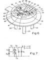
- Figure 6 is a perspective view of a pyroelectric radiation detector device in accordance with the second aspect of the invention and having a circuit configuration according to the circuit arrangement shown in Figure 5, and
- Figure 7 is a circuit diagram of another circuit arrangement in accordance with the first aspect of the invention.
- Referring now to Figures 1 and 2, there is shown a prior art pyroelectric radiation device comprising a body 1 of ceramic pyroelectric material, for example of modified lead zirconate titanate of approximately 3.5 mm x 3.0 mm x 50 micron thickness. On one major surface of the body there are a pair of
electrodes common electrode 4 consisting of nichrome. During manufacture of the device at a stage subsequent to the application of the electrodes to the body of pyroelectric material, a high field has been applied across the body, theelectrodes - The circuit connection of the device shown in Figures 1 and 2 is such that in operation only terminal connections to the
electrodes capacitive detectors 2, 4 (C1) and 3, 4 (C2), in which in the series connection the directions of polarisation of the pyroelectric material are in opposition, that is in terms of the capacitive detectors the normal signal voltages produced across the two elements. will be in opposition for a common radiation input. - Figure 3 shows a known circuit arrangement comprising a device as shown in Figures 1 and 2. The two series- connected
capacitive detectors electrode 2 of C, is connected to the gate of a field effect transistor (FET) and theelectrode 3 of C2 is connected to a point of reference potential. In one such known arrangement the FET element is incorporated in the same envelope as the detector device Cj, C2 and the resulting arrangement has only three terminals. - If one now considers the effect of subjecting the body 1 to an elevated temperature so that capacitive detectors C1 and C2 are uniformly affected then this will have the effect of generating voltages across the capacitive detectors C1 and C2 in a polarity sense which tends to increase the polarisation. Thus the
back electrode 4 becomes more positive and the front electrodes become more negative. Due to the same change in the temperature occurring for both elements the voltages generated in the series connected circuit will be in opposition and will therefore cancel out, although it should be noted that the floating back electrode may assume quite a high potential. - When following this heating the body 1 is cooled the opposite effect occurs. Thus the voltages generated across the capacitance detectors are in the opposite sense to the polarising field. Thus if on cooling, the
back electrode 4 becomes more negative relative to theelectrodes back electrode 4 will have leaked away with time prior to cooling and on cooling a depoling voltage will appear which will get larger as the temperature fall is increased. - It has been found that for a device of modified lead zirconate titanate material and having a configuration as shown in Figures 1 and 2 when subjecting the body 1 to temperature fluctuations of from -40°C to + 100°C the pre-induced poling of the element is severely degraded after several of such temperature excursions.
- Referring now to Figure 4, this circuit arrangement in accordance with the first aspect of the invention corresponds to the circuit shown in Figure 3 with the addition of the inclusion of two ultra-low leakage diodes D1 and D2 connected in series opposition and in parallel with the capacitive detector elements C1 and C2. There is also a further connection between the common point between C1 and C2 and the common point between D1 and D2. The diodes are connected in such a sense with respect to the directions of polarisation of the detector elements that for normal signal voltages produced across the detector elements for a common radiation input the diode elements are in the reverse direction. Thus in the arrangement shown the anodes of the diodes are connected to the negatively polarised sides of the detector elements. The operation of this circuit is such that in normal operating conditions the series connected diodes D1 and D2 present a high impedance between the FET gate and the point of constant potential so that their presence does not constitute a source of increased noise. However under the adverse temperature cycling conditions described and upon the cooling of the pyroelectric elements, the negative excursion at the common electrode corresponding to the common point between the capacitive elements relative to the electrodes at the opposite side of the elements is limited by virtue of both D1 and D2 being brought into a state of forward conduction. By suitable choice of the diode parameters this negative excursion may be limited, for example to a few hundred millivolts which is insufficient to bring about depoling of the previously poled elements.
- The circuit arrangement shown in Figure 4 can be embodied in a simple manner using a structure of the form shown in Figures 1 and 2, making an additional connection to the
back electrode 4 and including diode elements D, and D2. Such an arrangement may be present in part in the form of a two-terminal hybrid microcircuit including the detector elements C1 and C2 and the diode elements D, and D2 which is connected in operation to the FET. However it may be more convenient to include within the hybrid microcircuit the FET element and thus form a three terminal device. - Figure 5 shows a modified form of the circuit arrangement shown in Figure 4. It differs only in that between the gate of the FET (n-channel in this example) and the point of constant potential there is included a further ultra-low leakage diode element D3 in order to allow the gate leakage current to flow and hence stabilise the working point of the FET.
- Figure 6 shows a radiation detector device in accordance with the second aspect of the invention and in the form of a hybrid microcircuit having a circuit configuration of the form shown in Figure 5. The device comprises an envelope having a three
lead header 21 of TO-5 configuration as commonly used in the semiconductor art in which alead 22 is connected to the main metal part of the header and leads 23 and 24 extend as posts through said metal part and are insulated therefrom by metal-to-glass seals. The metal part of the header is gold- plated and on theupper surface 25 of the metal header there is aU-shaped plinth member 26 of approximately 1 mm thickness and consisting of high density alumina material having a gold coated upper surface. The plinth member forms a support for apyroelectric element 27 of modified lead zirconate titanate having a thickness of approximately 50 microns and major surfaces of approximately 3.0 mm x 3.5 mm. On the lower surface of theelement 27 there is an electrode of nichrome which forms an electrical connection to the gold coating on the plinth 26 by means of an intermediate layer of a conducting epoxy material. On the upper surface of theelement 27 there are twoelectrodes electrodes elements - The plinth member on one limb has a recessed
surface 33. The gold coating present on the upper surface of theplinth member 26 also extends to thesurface 33 and thus a conductive path is formed between these surfaces. On thesurface 33 there aresecured diode elements diode element 35 is connected to the gold platedheader surface 25 by means of a bondedwire 37 and the anode ofdiode element 34 is connected to thegold foil element 32 on theelectrode 30 by means of awire 38. Thegold foil element 31 on theelectrode 29 is connected to the gold plated header surface by awire 39. - The
diode elements Mullard type BAV 45 which is a very low leakage picoampere diode. These diode chips form the diode elements D, and D2 respectively in Figure 5. - Situated between the two
posts surface 25 there is analumina support member 41 of 2.0 mm x 2.0 mm x 0.25 mm having on its upper surface a conductive coating of gold. On the coated upper surface of themember 41 there is secured by means of a conducting epoxy layer an n-channel junction field effect transistor (JFET)element 42 in the form of an unencapsulated chip. In the chip the semiconductor substrate forms part of the gate electrode and at the upper surface there are source and drain bonding pads. The source and drain pads are connected by bondedwires leads member 41 and thegold foil element 32 on theelectrode 30 is formed by awire 46. In the circuit shown in Figure 5 this forms the connection between the gate G and the outer plate of C,. - Adjacent the
ceramic member 41 on thesurface 25 there is present afurther diode element 49 which is secured via its cathode to thesurface 25 with a conductive epoxy layer. The anode of thediode chip 49 is connected to the conductive surface on theceramic member 41 by awire 50. In this embodiment thediode chip 49, which corresponds to D3 in Figure 5, is also formed by anunencapsulated Mullard BAV 45 chip. - In the device shown all the wire connections are formed by. gold wires of 25 micron diameter and they are all secured to the various electrodes and surfaces by ultrasonic bonds.
- The pyroelectric radiation detector device shown in Figure 6, in the form of a three- terminal hybrid microcircuit may be employed effectively in intruder detector systems. The device is completed by a cover member (not shown) secured to the rim of the TO-5 header. The cover member has a window of multi-layer coated silicon which enables the transmission of infra-red radiation in a wavelength range of 6.5 microns to 14 microns. For further information on the further circuit connection of a detector device reference is invited to German Offenlegungsschrift No. 2,816,580 (PHB 32576). The JFET element within the device normally constitutes the input of amplifier means in which the high impedance on the input side is converted to a conventionally low output impedance. The provision of the depoling inhibiting diode elements enables the device to withstand considerable temperature cycling and also rapid cooling without degradation of the performance occurring due to the depoling of the pyroelectric element. In the manufacture of the particular detector shown the element has been poled by subjecting the
pyroelectric body 27, following application of the electrodes thereto, to a field of approximately 2 kV/mm, the field being maintained while cooling the body. It is to be noted that in the temperature cycling referred to or under adverse operational conditions the field strength to which the body is subjected on cooling may be comparatively high, the voltage at the electrode 28 in the absence of the depoling inhibiting diode elements possiby rising to 10 volts or in extreme cases up to 100 volts. - Figure 7 shows a further circuit arrangement in accordance with the invention and consisting of a modification of the arrangement shown in Figure 5. In this modified arrangement a further diode D4 is, having the same characteristics as diode D3' connected between the FET gate and the point of constant potential. It is found that the presence of the two diodes D3 and D4 in reverse parallel connection further enhances the stability of the operating point of the FET.
- It will be appreciated that many modifications are possible within the scope of this invention. In particular the structure shown in Figure 6 may be suitably modified when the initial polarising field applied to the
element 26 is such that the upper surface is positive and the lower surface is negative. In such a device the polarity of the depoling inhibiting diode element connections has to be reversed. Different circuit means may be employed for setting the operating point of the FET element, for example a high value resistor may be present between the FET gate and thecommon electrode terminal 22. - In some other circuit arrangements in accordance with the invention the depoling inhibiting diode elements may be formed by Schottky diodes.
- Although the embodiments of the circuit arrangement and detector device have been described in terms of a single pair of detector elements in which the structure and electrode connections are arranged to form two series connected capacitive detectors of which the directions of polarisation are in opposition, the invention may also be applied when using a greater number of detectors in which the structure and electrode connections yield more than two series connected capacitive detectors and of which the directions of polarisation of adjoining detectors in the series are in opposition for example detectors of the form as described in United States Patent Specification No. 3,842,276. In the application of the invention to such a detector, in general there will be a plurality of series connected ultra-low leakage diode elements corresponding in number and connected in parallel with the series connected detector elements.
- Although the embodiments of the invention have been described in terms of inhibiting the depoling of pairs of detector elements formed of a ceramic pyroelectric material, such as modified lead zirconate titanate, in which the polarisation is induced by application of a high field, the invention may also be employed where the elements are formed of materials having an inherent polarisation which is subject to depoling under the adverse conditions described.
Claims (8)
Applications Claiming Priority (2)
| Application Number | Priority Date | Filing Date | Title |
|---|---|---|---|
| GB7912912A GB2046431B (en) | 1979-04-12 | 1979-04-12 | Pyroelectric detector protection circuit |
| GB7912912 | 1979-04-12 |
Publications (2)
| Publication Number | Publication Date |
|---|---|
| EP0018033A1 EP0018033A1 (en) | 1980-10-29 |
| EP0018033B1 true EP0018033B1 (en) | 1982-12-08 |
Family
ID=10504532
Family Applications (1)
| Application Number | Title | Priority Date | Filing Date |
|---|---|---|---|
| EP80200310A Expired EP0018033B1 (en) | 1979-04-12 | 1980-04-08 | Radiation detector devices and circuit arrangements including radiation detector devices |
Country Status (7)
| Country | Link |
|---|---|
| US (1) | US4336452A (en) |
| EP (1) | EP0018033B1 (en) |
| JP (1) | JPS55141644A (en) |
| AU (1) | AU535269B2 (en) |
| CA (1) | CA1144776A (en) |
| DE (1) | DE3061253D1 (en) |
| GB (1) | GB2046431B (en) |
Families Citing this family (21)
| Publication number | Priority date | Publication date | Assignee | Title |
|---|---|---|---|---|
| JPS57203926A (en) * | 1981-06-09 | 1982-12-14 | Matsushita Electric Ind Co Ltd | Pyro-electric type infrared detection device |
| GB2102200B (en) * | 1981-07-17 | 1985-05-30 | Philips Electronic Associated | Infra-red radiation detector |
| EP0086369A1 (en) * | 1982-02-12 | 1983-08-24 | Cerberus Ag | Infrared intrusion detector with pyroelectric radiation receiver |
| GB2125214B (en) * | 1982-07-23 | 1985-10-02 | Philips Electronic Associated | Pyroelectric infra-red radiation detector |
| JPS60125530A (en) * | 1983-12-09 | 1985-07-04 | Kureha Chem Ind Co Ltd | Infrared ray sensor |
| US4648991A (en) * | 1984-05-30 | 1987-03-10 | Research Corporation | Pyroelectric crystals with high figures of merit |
| GB2170952B (en) * | 1985-02-08 | 1988-11-16 | Philips Electronic Associated | Infra-red radiation detector devices |
| GB2174224B (en) * | 1985-04-15 | 1988-07-13 | Philips Electronic Associated | Infra-red intruder detection system |
| DE3713642C2 (en) * | 1987-04-23 | 1994-01-20 | Deutsche Aerospace | Infrared pyrodetector system, suitable for temperature measurement of bodies |
| JPH01116419A (en) * | 1987-10-29 | 1989-05-09 | Sumitomo Metal Mining Co Ltd | Infrared detector |
| JPH01152226U (en) * | 1988-04-13 | 1989-10-20 | ||
| CH675921A5 (en) * | 1988-11-25 | 1990-11-15 | Cerberus Ag | |
| US5323025A (en) * | 1989-05-18 | 1994-06-21 | Murata Mfg. Co., Ltd. | Pyroelectric IR-sensor having a low thermal conductive ceramic substrate |
| JP2551249Y2 (en) * | 1993-11-08 | 1997-10-22 | 呉羽化学工業株式会社 | Pyroelectric device |
| US5485011A (en) * | 1994-01-28 | 1996-01-16 | Larry C. Y. Lee | Two-sided integrated-circuit PIR sensor package |
| US5626417A (en) * | 1996-04-16 | 1997-05-06 | Heath Company | Motion detector assembly for use with a decorative coach lamp |
| FR2817439B1 (en) * | 2000-11-30 | 2003-01-24 | Commissariat Energie Atomique | DEVICE FOR DETECTING INFRA RED RADIATION |
| EP1249690A1 (en) * | 2001-04-13 | 2002-10-16 | Francesco Porzio | Thermal detector |
| JP5533638B2 (en) * | 2010-12-24 | 2014-06-25 | セイコーエプソン株式会社 | Detection apparatus, sensor device, and electronic apparatus |
| US9939323B2 (en) * | 2012-12-28 | 2018-04-10 | Illinois Tool Works Inc. | IR sensor with increased surface area |
| JP7243638B2 (en) * | 2017-12-28 | 2023-03-22 | 株式会社村田製作所 | photodetector |
Citations (2)
| Publication number | Priority date | Publication date | Assignee | Title |
|---|---|---|---|---|
| US4110166A (en) * | 1975-11-19 | 1978-08-29 | Fujisawa Pharmaceutical Co., Ltd. | Process for the production of nocardicin A |
| US4110616A (en) * | 1976-01-16 | 1978-08-29 | Plessey Handel Und Investments A.G. | Pyroelectric detectors |
Family Cites Families (16)
| Publication number | Priority date | Publication date | Assignee | Title |
|---|---|---|---|---|
| US2122748A (en) * | 1935-02-27 | 1938-07-05 | Siemens Ag | Four-pole device containing nonlinear resistors |
| US3453432A (en) * | 1966-06-23 | 1969-07-01 | Barnes Eng Co | Pyroelectric radiation detector providing compensation for environmental temperature changes |
| US3539803A (en) * | 1967-12-21 | 1970-11-10 | Barnes Eng Co | Pyroelectric detector assembly |
| US3657644A (en) * | 1968-11-12 | 1972-04-18 | Nasa | Thermodielectric radiometer utilizing polymer film |
| US3480777A (en) * | 1969-02-28 | 1969-11-25 | Barnes Eng Co | Pyroelectric radiation detection system with extended frequency range and reduced capacitance |
| US3581092A (en) * | 1969-04-09 | 1971-05-25 | Barnes Eng Co | Pyroelectric detector array |
| US3631434A (en) * | 1969-10-08 | 1971-12-28 | Barnes Eng Co | Passive intrusion detector |
| JPS5651379B1 (en) * | 1971-04-07 | 1981-12-04 | ||
| US3842276A (en) * | 1973-06-15 | 1974-10-15 | Rca Corp | Thermal radiation detector |
| US4110116A (en) * | 1973-06-18 | 1978-08-29 | Minnesota Mining And Manufacturing Company | Fogged direct positive silver halide emulsion containing a cyanine dye having at least one benzoxazole or benzothiazole nucleus substituted with halogen atoms |
| US3839640A (en) * | 1973-06-20 | 1974-10-01 | J Rossin | Differential pyroelectric sensor |
| GB1447372A (en) * | 1973-06-21 | 1976-08-25 | Rank Organisation Ltd | Thermal radiation sensing conveyor particularly for a machine producing a roofing tile or the like |
| US3877308A (en) * | 1974-01-02 | 1975-04-15 | Minnesota Mining & Mfg | Pyroelectric temperature compensated sensing apparatus |
| US3940974A (en) * | 1974-05-06 | 1976-03-02 | Minnesota Mining And Manufacturing Company | Electrically compensated sensor |
| AT342126B (en) * | 1975-03-18 | 1978-03-10 | Gao Ges Automation Org | CIRCUIT ARRANGEMENT FOR EVALUATING SIGNALS, IN PARTICULAR OUTPUT SIGNALS OF OPTICAL MEASURING DEVICES |
| GB1580403A (en) * | 1977-04-19 | 1980-12-03 | Philips Electronic Associated | Pyroelectric detector circuits and devices |
-
1979
- 1979-04-12 GB GB7912912A patent/GB2046431B/en not_active Expired
-
1980
- 1980-04-03 US US06/137,028 patent/US4336452A/en not_active Expired - Lifetime
- 1980-04-08 DE DE8080200310T patent/DE3061253D1/en not_active Expired
- 1980-04-08 EP EP80200310A patent/EP0018033B1/en not_active Expired
- 1980-04-09 AU AU57250/80A patent/AU535269B2/en not_active Ceased
- 1980-04-09 JP JP4579080A patent/JPS55141644A/en active Granted
- 1980-04-10 CA CA000349578A patent/CA1144776A/en not_active Expired
Patent Citations (2)
| Publication number | Priority date | Publication date | Assignee | Title |
|---|---|---|---|---|
| US4110166A (en) * | 1975-11-19 | 1978-08-29 | Fujisawa Pharmaceutical Co., Ltd. | Process for the production of nocardicin A |
| US4110616A (en) * | 1976-01-16 | 1978-08-29 | Plessey Handel Und Investments A.G. | Pyroelectric detectors |
Also Published As
| Publication number | Publication date |
|---|---|
| CA1144776A (en) | 1983-04-19 |
| JPS6125297B2 (en) | 1986-06-14 |
| DE3061253D1 (en) | 1983-01-13 |
| JPS55141644A (en) | 1980-11-05 |
| GB2046431A (en) | 1980-11-12 |
| GB2046431B (en) | 1983-06-15 |
| AU535269B2 (en) | 1984-03-08 |
| EP0018033A1 (en) | 1980-10-29 |
| AU5725080A (en) | 1980-10-16 |
| US4336452A (en) | 1982-06-22 |
Similar Documents
| Publication | Publication Date | Title |
|---|---|---|
| EP0018033B1 (en) | Radiation detector devices and circuit arrangements including radiation detector devices | |
| US4110616A (en) | Pyroelectric detectors | |
| US3585415A (en) | Stress-strain transducer charge coupled to a piezoelectric material | |
| US3294988A (en) | Transducers | |
| US4788581A (en) | MOS dosimeter | |
| US3539803A (en) | Pyroelectric detector assembly | |
| US3896309A (en) | Radiation detecting device | |
| US4255756A (en) | Substrate bias generator | |
| US4678916A (en) | Dosimeter | |
| US4198564A (en) | Pyroelectric detector circuits and devices | |
| US4258259A (en) | Infrared detector | |
| JPS6038623A (en) | Detector for infrared ray | |
| US4214165A (en) | Pyroelectric IR detector with signal capacitively coupled to an output circuit | |
| US4437003A (en) | Differential pyroelectric sensor with static discharge | |
| US3932753A (en) | Pyroelectric device with coplanar electrodes | |
| US5034608A (en) | Infrared sensor operable without cooling | |
| Bauer et al. | A simple technique to interface pyroelectric materials with silicon substrates for infrared detection | |
| US3622712A (en) | Device employing selenium-semiconductor heterojunction | |
| US3448348A (en) | Transducer utilizing electrically polarizable material | |
| EP0102101B1 (en) | Pyroelectric infra-red radiation detector | |
| EP0070601B1 (en) | Infra-red radiation detector | |
| US3624465A (en) | Heterojunction semiconductor transducer having a region which is piezoelectric | |
| JP2599354B2 (en) | Infrared detector | |
| Bravina et al. | Pyroelectricity: some new research and application aspects | |
| US3789369A (en) | Thin film mis storage diode |
Legal Events
| Date | Code | Title | Description |
|---|---|---|---|
| PUAI | Public reference made under article 153(3) epc to a published international application that has entered the european phase |
Free format text: ORIGINAL CODE: 0009012 |
|
| AK | Designated contracting states |
Designated state(s): CH DE FR GB IT SE |
|
| 16A | New documents despatched to applicant after publication of the search report | ||
| 17P | Request for examination filed |
Effective date: 19801127 |
|
| ITF | It: translation for a ep patent filed |
Owner name: ING. C. GREGORJ S.P.A. |
|
| GRAA | (expected) grant |
Free format text: ORIGINAL CODE: 0009210 |
|
| AK | Designated contracting states |
Designated state(s): CH DE FR GB IT SE |
|
| REF | Corresponds to: |
Ref document number: 3061253 Country of ref document: DE Date of ref document: 19830113 |
|
| ET | Fr: translation filed | ||
| PGFP | Annual fee paid to national office [announced via postgrant information from national office to epo] |
Ref country code: CH Payment date: 19840720 Year of fee payment: 5 |
|
| PGFP | Annual fee paid to national office [announced via postgrant information from national office to epo] |
Ref country code: SE Payment date: 19890426 Year of fee payment: 10 |
|
| ITTA | It: last paid annual fee | ||
| PG25 | Lapsed in a contracting state [announced via postgrant information from national office to epo] |
Ref country code: LI Effective date: 19890430 Ref country code: CH Effective date: 19890430 |
|
| REG | Reference to a national code |
Ref country code: CH Ref legal event code: PL |
|
| PG25 | Lapsed in a contracting state [announced via postgrant information from national office to epo] |
Ref country code: SE Effective date: 19900409 |
|
| PGFP | Annual fee paid to national office [announced via postgrant information from national office to epo] |
Ref country code: GB Payment date: 19920401 Year of fee payment: 13 |
|
| PGFP | Annual fee paid to national office [announced via postgrant information from national office to epo] |
Ref country code: FR Payment date: 19920422 Year of fee payment: 13 |
|
| PGFP | Annual fee paid to national office [announced via postgrant information from national office to epo] |
Ref country code: DE Payment date: 19920623 Year of fee payment: 13 |
|
| PG25 | Lapsed in a contracting state [announced via postgrant information from national office to epo] |
Ref country code: GB Effective date: 19930408 |
|
| GBPC | Gb: european patent ceased through non-payment of renewal fee |
Effective date: 19930408 |
|
| PG25 | Lapsed in a contracting state [announced via postgrant information from national office to epo] |
Ref country code: FR Effective date: 19931229 |
|
| PG25 | Lapsed in a contracting state [announced via postgrant information from national office to epo] |
Ref country code: DE Effective date: 19940101 |
|
| REG | Reference to a national code |
Ref country code: FR Ref legal event code: ST |
|
| EUG | Se: european patent has lapsed |
Ref document number: 80200310.3 Effective date: 19910110 |
|
| PLBE | No opposition filed within time limit |
Free format text: ORIGINAL CODE: 0009261 |
|
| STAA | Information on the status of an ep patent application or granted ep patent |
Free format text: STATUS: NO OPPOSITION FILED WITHIN TIME LIMIT |