EP0010657B1 - Selektives Ätzen von polymeren, Silicone enthaltenden Stoffen in einem reaktiven Plasma - Google Patents
Selektives Ätzen von polymeren, Silicone enthaltenden Stoffen in einem reaktiven Plasma Download PDFInfo
- Publication number
- EP0010657B1 EP0010657B1 EP79103897A EP79103897A EP0010657B1 EP 0010657 B1 EP0010657 B1 EP 0010657B1 EP 79103897 A EP79103897 A EP 79103897A EP 79103897 A EP79103897 A EP 79103897A EP 0010657 B1 EP0010657 B1 EP 0010657B1
- Authority
- EP
- European Patent Office
- Prior art keywords
- layer
- plasma
- silicon
- silicone
- torr
- Prior art date
- Legal status (The legal status is an assumption and is not a legal conclusion. Google has not performed a legal analysis and makes no representation as to the accuracy of the status listed.)
- Expired
Links
Images
Classifications
-
- H—ELECTRICITY
- H10—SEMICONDUCTOR DEVICES; ELECTRIC SOLID-STATE DEVICES NOT OTHERWISE PROVIDED FOR
- H10P—GENERIC PROCESSES OR APPARATUS FOR THE MANUFACTURE OR TREATMENT OF DEVICES COVERED BY CLASS H10
- H10P50/00—Etching of wafers, substrates or parts of devices
- H10P50/20—Dry etching; Plasma etching; Reactive-ion etching
- H10P50/28—Dry etching; Plasma etching; Reactive-ion etching of insulating materials
- H10P50/286—Dry etching; Plasma etching; Reactive-ion etching of insulating materials of organic materials
- H10P50/287—Dry etching; Plasma etching; Reactive-ion etching of insulating materials of organic materials by chemical means
Definitions
- This invention relates to the selective plasma chemical etching of polyimide-silicone copolymers for patterning thereof.
- a method of making polyimide-silicone copolymers and their application to selective surface areas of electronic devices, e.g., semiconductor junctions, is known. After the copolymer material is applied to such surface areas it becomes necessary on occasion to open windows in the coating and/or to remove material from selective areas. It is desirable that the removal of the unwanted portions of the copolymer material be done as quickly and as easily as possible to facilitate semiconductor device processing. It is also most desirable to maintain the registry and dimensions of the pattern.
- U.S. Patent 4,140,572 describes a method as per the preamble of claim 1. Said method uses titanum as a masking material for etching with a phenol-bearing solution. However, although the process is successful, one always finds a need for a more efficient process for a particular manufacturing requirement.
- a novel process introduced into the semiconductor art is chemical etching by use of plasma.
- the plasma is an ionized gas containing a variety of highly reactive particles such, for example, as ions, free electrons and free radicals.
- An article entitled "A Survey of Plasma-Etching Process” appeared in Solid State Technology, May 1976, and describes the process.
- FR-A-2 309 976 describes a method for making a network of interconnected conductors on a substrate consisting of silicon. For carrying out said method there is arranged a second polymer layer between a first polymer layer and a masking layer. While the first polymer layer consists of a polyimide, the second polymer layer consists of a polysulphone.
- the copolymer used according to the invention comprises a component being etchable by the oxygen containing CF 4- plasma - namely the polyimide - and a component being resistant against being etched by said oxygen containing CF 4- plasma. Consequently it cannot have been obvious for the expert how the copolymer of both said components would behave with respect to being etched by an oxygen containing CF 4 plasma.
- a new and improved method for patterning a layer of cured silicone-polyimide copolymer material disposed on the surface of the body is a method employed when the material is disposed on the surface of a body of semiconductor material
- the layer is from 10- 4 to 10- 3 cm (1 to 10 microns) in thickness.
- the final cure is accomplished by baking at about 450°C.
- a layer of silicon, preferably, of the order of 10- 5 cm (1000 A) is disposed on the copolymer material layer by electron beam deposition technique.
- a layer of either negative or positive photoresist material is disposed on the silicon material which is to act as a mask.
- the layer of photoresist material is processed to form one or more windows therein. Selected surface areas of the layer of silicon are exposed in the windows.
- the exposed silicon is chemically etched by a plasma of Freon 14, which is a tradename of E.I. DuPont de Nemours & Co., Inc. for CF 4 , containing about 4% oxygen by volume of Freon 14 for a sufficient time to open windows in the silicon layer.
- the windows are aligned with those in the photoresist layer thereby enabling selected surface areas of the copolymer material to be exposed in the windows.
- the layer of photoresist is preferably simultaneously stripped with the etching of the polyimide-silicone copolymer material.
- the copolymer material is chemically etched in a plasma of oxygen. Chemical etching is performed until windows are opened in the layer to expose surface areas of the body thereat. The processed body is then cleaned, as required, and further processed into the required semiconductor device.
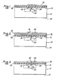
- Figures 1 through 6 are side elevation views, partly in cross-section of a body of semiconductor material processed in accordance with the teachings of this invention.
- polyimide-silicone copolymer is the reaction product of a silicon-free organic diamine, an organic tetracarboxylic dianhydride and a polysiloxane diamine which is a polymer precursor soluble in a suitable organic solvent.
- R is preferably an optionally substituted alkalene radical such as one comprising 2 to 8 carbon atoms or an optionally substituted arylene radical such as one comprising 6-15 carbon atoms. Most preferably R is an optionally substituted alkylene radical having 2 to 4 carbon atoms or an optionally substituted arylene radical having 6 to 9 carbon atoms.
- R' is preferably an optionally substituted alkyl radical such as one comprising 1 to 8 carbon atoms or an optionally substituted aryl radical such as one comprising 6 to 1 5 carbon atoms.
- R' is most preferably an optionally substituted alkyl radical having 1 to 4 carbon atoms or an optionally substituted aryl radical having 6 to 9 carbon atoms.
- Q is preferably an optionally substituted alkylene radical having 2 to 20 carbon atoms and most preferably having 6 to 18 carbon atoms or an optionally substituted arylene radical having 6 to 15 carbon atoms or an optionally substituted cycloalkyl radical having 5 to 7 carbon.
- n and m are integers preferably different integers from 100 to 1000.
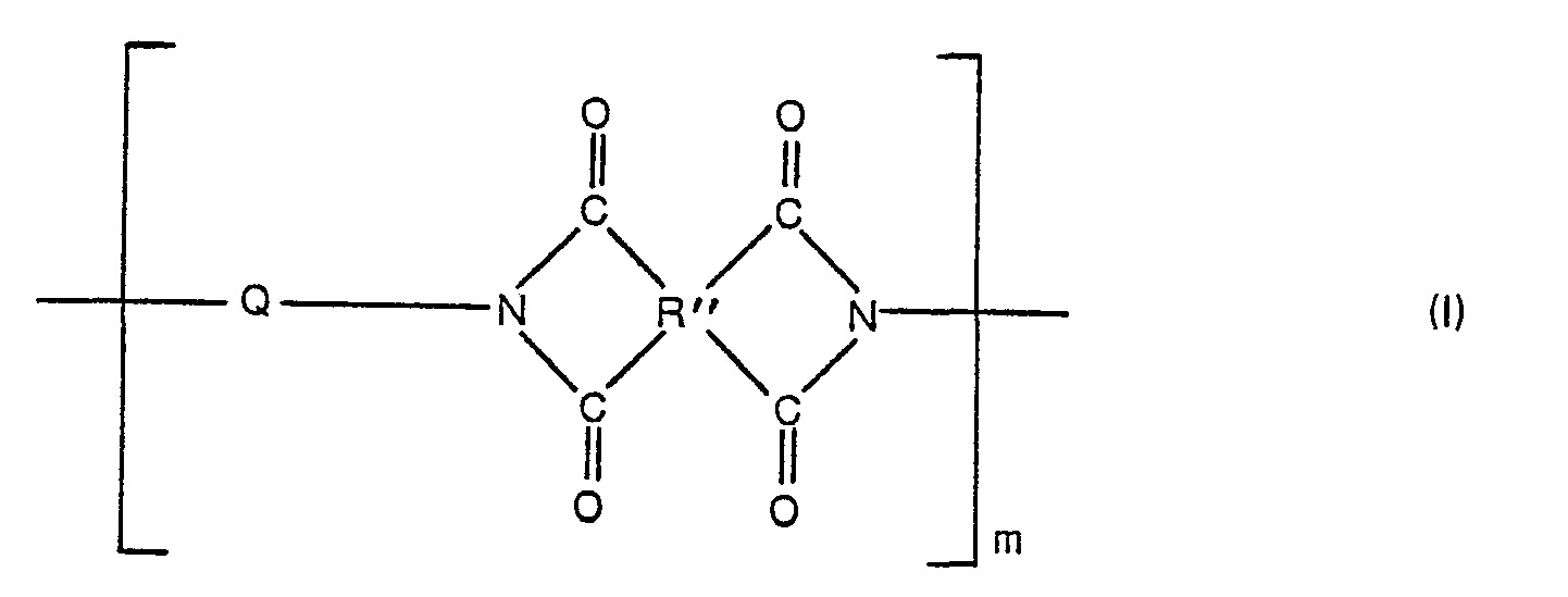
- the above-mentioned random and block copolymers can be prepared by effecting reaction, in the proper molar proportions, of a mixture of ingredients comprising a diaminosiloxane of the general formula: a silicon-free diamine compound of the formula: and a tetracarboxylic acid dianhydride having the formula: wherein R, R', R", Q and x have the meanings given above.
- a polysiloxane-imide composition may be used with comparable effectiveness by blending together a polyimide composed solely of recurring structural units of Formula I with a polyimide composed solely of recurring structural units of Formula II employing the polyimide of Formula II in such a molar proportion that the structural units of the latter are within. the range of from 5 to 50 mol percent of said units based on the total molar concentration of the units of Formula I.
- the ultimate polyimide siloxane composition used in the practice of this invention will consist essentially of the imido structures found in Formulas I and II.
- the actual precursor materials resulting from the reaction of the diaminosiloxane, the silicon-free organic diamine and the tetracarboxylic acid dianhydride will initially be in the form of a polyamic acid structure composed of structural units of the formulas: where R, R', R", Q, x, m and n have the meanings given above.
- diamino siloxanes of Formula III which may be used in the practice of the present invention include compounds having the following formulas: and the like.
- diamines of Formula IV above are described in the prior art and are to a large extent commercially available materials. Typical of such diamines from which the prepolymer may be prepared are the following:
- the tetracarboxylic acid dianhydrides of Formula V may further be defined in that the R" is a tetravalent radical, e.g. a radical derived from or containing an aromatic group containing at least 6 carbon atoms characterized by benzenoid unsaturation, wherein each of the 4 carbonyl groups of the dianhydride are attached to a separate carbon atom in the tetravalent radical, the carbonyl groups being in pairs in which the groups in each pair are attached to adjacent carbon atoms of the R" radical or to carbon atoms in the R" radical at most one carbon atom removed, to provide a 5-membered or 6- membered ring as follows:
- a suitable solvent including, for example, N-methyl-pyrrolidone, N,N-dimethylacetamide, N,N-dimethylformamide, etc.
- a suitable solvent including, for example, N-methyl-pyrrolidone, N,N-dimethylacetamide, N,N-dimethylformamide, etc.
- the block copolymers or blends of polymers may be dried in an initial heating step at temperatures of about 75 to 125°C for a sufficient time frequently under vacuum to remove the solvent.
- the polyamic acid is then converted to the corresponding polyimide- siloxane by heating at temperatures of about 150°C-300°C for a sufficient time to effect the desired conversion to the polyimide structure and final cure.
- a preferred curing cycle for materials of the above general formula is as follows:
- an additional layer of the material is preferably applied after the first curing step (a). More than one additional layer can be applied in this manner with a subsequent curing step (a) after each new layer of silicone-polyimide copolymer material is applied to the previous layer.
- the final curing steps (b), (c) and (d) are then practiced.
- a body 10 of semiconductor material of N-type conductivity having opposed major surfaces 12 and 14 is proposed to form regions 16 and 18 of P and N type conductivity respectively therein.
- P-N junctions 20 and 22 are formed at the abutting, contiguous surfaces of the regions 16 and the body 10 and regions 16 and 18, respectively. End portions of the P-N junctions 16 and 18 are exposed at the surface 12.
- the material of the body 10 may be silicon, silicon carbide, germanium, gallium arsenide, a compound of a Group III element and a Group V element. In order to illustrate the novel process of this invention the material of the body is said to be of silicon.
- An electrical contact 24 is affixed to the region 16 and is in ohmic electrical contact therewith.
- An ohmic electrical contact 26 is affixed to the region 18.
- Ohmic contacts 24 and 26 are typically made of aluminum.
- a layer 28 of the cured silicone-polyimide copolymer material is disposed on the surface 12 and the contacts 24 and 26. Although the thickness of the layer 28 may be of the order of 10- 3 cm (10 microns) or more, a thickness of from 10- 4 to 5. 10-1 cm (1 to 5 microns) is preferred.
- a layer 30 of silicon is vapor deposited upon the layer 28 of cured silicone-polyimide copolymer material preferably from a source of high purity silicon.
- a thickness of from 5.10- 5 cm (100 A to 2000 A) of the layer 30 has been found to be satisfactory as a suitable mask for selective plasma chemical etching of the material of the layer 28.
- the layer 30 is of the order of 10- 5 cm (1000 A) in thickness.
- a layer 32 of a photoresist material is disposed on the layer 30 of silicon.
- the photoresist material is a positive material such, for example, as OFPR-2 from Tokyo Ohka America, Inc.
- the photoresist is pre-cured by 15 minutes of air drying at room temperature followed by baking at 90°C, approximately for a period of 30 minutes in nitrogen.
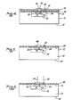
- a suitable mask is disposed on the photoresist layer 32, properly aligned in order that the windows to be opened in the silicone-polyimide material layer 28 are oriented properly with respect to contacts 24 and 26.
- the masked layer 32 of photoresist is exposed to ultraviolet radiation for the proper length of time.
- the exposed layer 32 removes unfixed photoresist material from the window areas 36 and 38 of the layer 32. The remainder of the material of the layer 32 is "fixed".
- the exposed layer 32 may be post cured by 140°C bake for 30 minutes in order to enhance its adhesion to the silicon layer.
- the processed wafer 10 is placed in a suitable plasma etching machine, not shown, such for example, as an IPC series 4000, manufactured by International Plasma Corporation.
- the processed wafer 10 is placed in the work chamber of the plasma etching machine and the chamber is then evacuated.
- the processed wafer 10 is preheated in the chamber in a nitrogen plasma formed at an RF power of a range of 100 watts to 200 watts of energy and from 65 to 80 Pascal (0.5 torr to 0.6 torr) for a period of about 3 minutes to bring the temperature of the processed body 10 to about 75°C and the nitrogen plasma is turned off.
- the preheating step is practiced to bring the body 10 up to the reaction temperature required for etching in a most uniform manner.
- the desired reaction temperature ranges from 65°C to 85°C.
- CF 4 including 4% oxygen by volume at a gas flow rate of from 1 OOcc/minute to 1 50cc/minute is introduced and a plasma is formed at an energy level of about 100 watts.
- the pressure in the chamber is typically 40 to 65 Pascal (0.3 to 0.5 torr).
- This new plasma is employed to etch the exposed silicon layer 30 at a rate of from 5.10-6 to 10- 5 cm (0.5 x 10 3 A to 1 x 10 3 A) per minute.
- Plasma etching is practiced for a sufficient time to remove the exposed silicon, or for about one to two minutes, to assure complete removal of the silicon to open windows 42 and 44 ( Figure 3) in the silicon to expose selected surface areas of the silicon-polyimide copolymer material therein.
- the previous plasma of CF 4 and oxygen is stopped.
- a new plasma of oxygen is initiated.
- the RF power is from 200 watts to 400 watts. About 300 watts is preferred.
- the gas flow rate is about 300 CCPM of oxygen to obtain a chamber pressure of preferably about 215 Pascal (1.6 torr). However, the chamber pressure may range from 105 to 265 Pascal (0.8 torr to 2.0 torr).
- These conditions for the plasma are sufficient to etch away the exposed silicone-polyimide material exposed in the windows 42 and 44 of the silicon mask 32.
- the etch rate of the polyimide-silicone copolymer material is from 0.25 to 0.5.10- 4 cm (micron) per minute under the stipulated conditions.
- the oxygen plasma strips away the photoresist of the mask layer 32. Removal of the silicone-polyimide material produces windows 48 and 50 to expose the electrical contacts 26 and 24 therein as shown in Figure 4.
- the plasma is turned off.
- the chamber is evacuated and a new plasma is formed, the composition being CF 4 and oxygen, the same as initially formed for etching the windows in the silicon layer 30.
- the remainder of the material of the silicon mask layer 30 is removed by the plasma etchant in about one minute.
- the plasma is turned off, the chamber is brought again to atmospheric pressure and the processed body 10 removed from the chamber.
- the processed body 10 is as shown in Figure 5.
- the processed body may then be further cleaned by aqueous solutions if necessary.
- the body 10 may now be processed further as required by affixing electrical leads 54 and 56 to the respective electrical contacts 26 and 24 as illustrated in Figure 6.
- any exposed areas of silicon on the body 10 will be etched by an amount closely related to the thickness of the masking layer 30.
- a polymer precursor solution was formed by reacting benzophenone tetracarboxylic acid dianhydride with methylene dianiline and bis(a-aminopropyl)tetramethyldisiloxane, the latter two diamine materials being present in the molar ratio of 70:30.
- the reaction was carried out at a temperature of less than 50°C and using suitably purified and dried materials to favor a large molecular weight polymer.
- a solution of the polymer precursor in the form of the polyamic acid form dissolved in N-methyl-2-pyrrolidone containing 25% solids by weight was disposed on the surface of the devices. About 7 to 10 drops of the precursor solution was disposed on the surface of the wafers, and therefore the devices.
- the wafers were then spun at from about 2000RPM to about 3000RPM for 20 seconds.
- the coated wafers were cured at 150°C ⁇ 5°C for about 30 minutes in Nitrogen, 185°C ⁇ 5°C in Nitrogen for about 30 minutes, at 225°C ⁇ 5°C in a vacuum of 9.8 ⁇ 10 4 Pascal (29" Hg) for about 2 hours and at 450°C ⁇ 5°C in nitrogen for ten minutes.
- the layer of copolymer material was from 1.5 to 2.0.10-4 cm (microns) in thickness when cured.
- a layer of positive photoresist material was deposited on the silicon layer and processed to open windows therein.
- the processed wafer was placed in an IPC series 4000 plasma etching machine. The wafer was preheated in a nitrogen plasma at 100 watts and 65 Pascal (0.5 torr) for 3 minutes.
- the exposed portions of the silicon layer in the windows of the photoresist material were etched by a plasma consisting of CF 4 with 4% oxygen (100 CCPM) at 100 watts and a total pressure of about 40 Pascal (0.3 torr).
- the elapsed etching time for the silicon was one minute.
- the plasma was turned off and the chamber was evacuated.
- An oxygen plasma was then established at 300 watts of RF power, 300 CCPM of oxygen at a pressure of about 215 Pascal (1.6 torr).
- the polyimide-silicone copolymer exposed in the silicon windows was etched in 5 minutes. The remaining photoresist material was removed simultaneously during the etching of the copolymer material. After etching of the polyimide-silicone copolymer material was completed, the plasma was turned off and evacuated.
- CF 4 , 4% oxygen plasma was again established at 100 watts RF power and about 40 Pascal (0.3 torr).
- the new plasma was employed to etch the remaining silicon material of the mask from the copolymer material. Etching of the silicon was completed in one minute. The plasma was turned off and the chamber was brought back to atmospheric pressure. The processed body was removed and examined.
- the exposed aluminum contact surface did not show any sign of attack by the plasma etchants.
- the windows were well defined and had dimensional stability.
- the edges of the copolymer material were not visibly undercut.
Landscapes
- Drying Of Semiconductors (AREA)
- Macromolecular Compounds Obtained By Forming Nitrogen-Containing Linkages In General (AREA)
- Treatments Of Macromolecular Shaped Articles (AREA)
- Physical Or Chemical Processes And Apparatus (AREA)
- Formation Of Insulating Films (AREA)
Claims (12)

Applications Claiming Priority (2)
| Application Number | Priority Date | Filing Date | Title |
|---|---|---|---|
| US05/952,406 US4209356A (en) | 1978-10-18 | 1978-10-18 | Selective etching of polymeric materials embodying silicones via reactor plasmas |
| US952406 | 1978-10-18 |
Publications (2)
| Publication Number | Publication Date |
|---|---|
| EP0010657A1 EP0010657A1 (de) | 1980-05-14 |
| EP0010657B1 true EP0010657B1 (de) | 1984-09-19 |
Family
ID=25492879
Family Applications (1)
| Application Number | Title | Priority Date | Filing Date |
|---|---|---|---|
| EP79103897A Expired EP0010657B1 (de) | 1978-10-18 | 1979-10-11 | Selektives Ätzen von polymeren, Silicone enthaltenden Stoffen in einem reaktiven Plasma |
Country Status (5)
| Country | Link |
|---|---|
| US (1) | US4209356A (de) |
| EP (1) | EP0010657B1 (de) |
| JP (1) | JPS5577137A (de) |
| DE (1) | DE2967224D1 (de) |
| IE (1) | IE49016B1 (de) |
Families Citing this family (27)
| Publication number | Priority date | Publication date | Assignee | Title |
|---|---|---|---|---|
| DE2945854A1 (de) * | 1979-11-13 | 1981-05-21 | Deutsche Itt Industries Gmbh, 7800 Freiburg | Ionenimplantationsverfahren |
| JPS5760330A (en) * | 1980-09-27 | 1982-04-12 | Fujitsu Ltd | Resin composition |
| US4353777A (en) * | 1981-04-20 | 1982-10-12 | Lfe Corporation | Selective plasma polysilicon etching |
| GB2126786B (en) * | 1982-09-04 | 1986-04-03 | Emi Ltd | Ion sensitive field effect transistor encapsulation |
| FR2535525A1 (fr) * | 1982-10-29 | 1984-05-04 | Western Electric Co | Procede de fabrication de circuits integres comportant des couches isolantes minces |
| GB2137808A (en) * | 1983-04-06 | 1984-10-10 | Plessey Co Plc | Integrated circuit processing method |
| US4482427A (en) * | 1984-05-21 | 1984-11-13 | International Business Machines Corporation | Process for forming via holes having sloped walls |
| US4723978A (en) * | 1985-10-31 | 1988-02-09 | International Business Machines Corporation | Method for a plasma-treated polysiloxane coating |
| US4866508A (en) * | 1986-09-26 | 1989-09-12 | General Electric Company | Integrated circuit packaging configuration for rapid customized design and unique test capability |
| US4937203A (en) * | 1986-09-26 | 1990-06-26 | General Electric Company | Method and configuration for testing electronic circuits and integrated circuit chips using a removable overlay layer |
| US4714516A (en) * | 1986-09-26 | 1987-12-22 | General Electric Company | Method to produce via holes in polymer dielectrics for multiple electronic circuit chip packaging |
| US5094709A (en) * | 1986-09-26 | 1992-03-10 | General Electric Company | Apparatus for packaging integrated circuit chips employing a polymer film overlay layer |
| US4783695A (en) * | 1986-09-26 | 1988-11-08 | General Electric Company | Multichip integrated circuit packaging configuration and method |
| US4835704A (en) * | 1986-12-29 | 1989-05-30 | General Electric Company | Adaptive lithography system to provide high density interconnect |
| EP0658416B1 (de) * | 1993-11-23 | 2001-02-07 | Dyconex Patente Ag | Verfahren zur Strukturierung von Polymerfolien |
| US5891761A (en) * | 1994-06-23 | 1999-04-06 | Cubic Memory, Inc. | Method for forming vertical interconnect process for silicon segments with thermally conductive epoxy preform |
| US5657206A (en) * | 1994-06-23 | 1997-08-12 | Cubic Memory, Inc. | Conductive epoxy flip-chip package and method |
| US6255726B1 (en) | 1994-06-23 | 2001-07-03 | Cubic Memory, Inc. | Vertical interconnect process for silicon segments with dielectric isolation |
| US5675180A (en) | 1994-06-23 | 1997-10-07 | Cubic Memory, Inc. | Vertical interconnect process for silicon segments |
| US6080596A (en) * | 1994-06-23 | 2000-06-27 | Cubic Memory Inc. | Method for forming vertical interconnect process for silicon segments with dielectric isolation |
| US6124633A (en) * | 1994-06-23 | 2000-09-26 | Cubic Memory | Vertical interconnect process for silicon segments with thermally conductive epoxy preform |
| US6486528B1 (en) | 1994-06-23 | 2002-11-26 | Vertical Circuits, Inc. | Silicon segment programming apparatus and three terminal fuse configuration |
| US5698895A (en) * | 1994-06-23 | 1997-12-16 | Cubic Memory, Inc. | Silicon segment programming method and apparatus |
| AUPO281896A0 (en) * | 1996-10-04 | 1996-10-31 | Unisearch Limited | Reactive ion etching of silica structures for integrated optics applications |
| JP2004247675A (ja) * | 2003-02-17 | 2004-09-02 | Renesas Technology Corp | 半導体装置の製造方法 |
| JP2019029556A (ja) * | 2017-08-01 | 2019-02-21 | 旭化成株式会社 | 半導体装置、及びその製造方法 |
| TWI707889B (zh) * | 2017-08-01 | 2020-10-21 | 日商旭化成股份有限公司 | 半導體裝置及其製造方法 |
Family Cites Families (10)
| Publication number | Priority date | Publication date | Assignee | Title |
|---|---|---|---|---|
| US3586554A (en) * | 1969-01-15 | 1971-06-22 | Ibm | Process for increasing photoresist adhesion to a semiconductor by treating the semiconductor with a disilylamide |
| US3816198A (en) * | 1969-09-22 | 1974-06-11 | G Babcock | Selective plasma etching of organic materials employing photolithographic techniques |
| US3767490A (en) * | 1971-06-29 | 1973-10-23 | Ibm | Process for etching organic coating layers |
| US3975252A (en) * | 1975-03-14 | 1976-08-17 | Bell Telephone Laboratories, Incorporated | High-resolution sputter etching |
| US3985597A (en) * | 1975-05-01 | 1976-10-12 | International Business Machines Corporation | Process for forming passivated metal interconnection system with a planar surface |
| US3994817A (en) * | 1975-07-28 | 1976-11-30 | Rockwell International Corporation | Etchant for etching silicon |
| US4040874A (en) * | 1975-08-04 | 1977-08-09 | General Electric Company | Semiconductor element having a polymeric protective coating and glass coating overlay |
| US3986912A (en) * | 1975-09-04 | 1976-10-19 | International Business Machines Corporation | Process for controlling the wall inclination of a plasma etched via hole |
| JPS52104066A (en) * | 1976-02-27 | 1977-09-01 | Hitachi Ltd | Selective etching method of thermosetting organic materials |
| US4140572A (en) * | 1976-09-07 | 1979-02-20 | General Electric Company | Process for selective etching of polymeric materials embodying silicones therein |
-
1978
- 1978-10-18 US US05/952,406 patent/US4209356A/en not_active Expired - Lifetime
-
1979
- 1979-10-01 IE IE1864/79A patent/IE49016B1/en unknown
- 1979-10-11 DE DE7979103897T patent/DE2967224D1/de not_active Expired
- 1979-10-11 EP EP79103897A patent/EP0010657B1/de not_active Expired
- 1979-10-17 JP JP13302079A patent/JPS5577137A/ja active Pending
Also Published As
| Publication number | Publication date |
|---|---|
| IE791864L (en) | 1980-04-18 |
| EP0010657A1 (de) | 1980-05-14 |
| JPS5577137A (en) | 1980-06-10 |
| DE2967224D1 (en) | 1984-10-25 |
| IE49016B1 (en) | 1985-07-10 |
| US4209356A (en) | 1980-06-24 |
Similar Documents
| Publication | Publication Date | Title |
|---|---|---|
| EP0010657B1 (de) | Selektives Ätzen von polymeren, Silicone enthaltenden Stoffen in einem reaktiven Plasma | |
| US4140572A (en) | Process for selective etching of polymeric materials embodying silicones therein | |
| US4017340A (en) | Semiconductor element having a polymeric protective coating and glass coating overlay | |
| US4430153A (en) | Method of forming an RIE etch barrier by in situ conversion of a silicon containing alkyl polyamide/polyimide | |
| US4040874A (en) | Semiconductor element having a polymeric protective coating and glass coating overlay | |
| Diaham | Polyimide in Electronics: Applications and Processability | |
| US5137751A (en) | Process for making thick multilayers of polyimide | |
| EP0194865A2 (de) | Löslicher Polyimid-Siloxan-Vorläufer, Verfahren zu seiner Herstellung und vernetztes Polyimid-Siloxan | |
| GB2204316A (en) | Photopatterning silicone polyamic acids, dye compositions, and colour filters | |
| EP0603339A1 (de) | Polyimidcopolymere die 3,3', 4,4'-tetracarboxydiphenyldianhydrideinheiten enthalten | |
| EP0247084A1 (de) | Verfahren zur herstellung von polyimiden von hohem molekulargewicht, produkt und dessen verwendung | |
| US4198444A (en) | Method for providing substantially hermetic sealing means for electronic components | |
| JPS6314452A (ja) | 半導体装置 | |
| US5426071A (en) | Polyimide copolymer film for lift-off metallization | |
| US4331970A (en) | Use of dispersed solids as fillers in polymeric materials to provide material for semiconductor junction passivation | |
| EP0448252A1 (de) | Polyimidcopolymere die 4-4'-Bis(aminophenoxy)biphenyl- und Diaminosiloxaneinheiten enthalten | |
| JPS584816B2 (ja) | 半導体素子とその製法 | |
| EP0448248B1 (de) | Verfahren zur Herstellung von dicken Multilayer aus Polyimid | |
| EP0209670B1 (de) | Verfahren zum Flachmachen eines Substrats | |
| NL7906941A (nl) | Halfgeleidercomponent. | |
| US4215157A (en) | Process for preparing polyetherimide coatings | |
| US5451655A (en) | Process for making thermostable coating materials | |
| GB1571999A (en) | Semiconductors | |
| US5660920A (en) | Inter-level dielectrics with low dielectric constants | |
| NL7906939A (nl) | Vulstof bevattend polymeer materiaal voor het bekleden van halfgeleidercomponenten, alsmede met dit polymere materiaal beklede halfgeleidercomponenten. |
Legal Events
| Date | Code | Title | Description |
|---|---|---|---|
| PUAI | Public reference made under article 153(3) epc to a published international application that has entered the european phase |
Free format text: ORIGINAL CODE: 0009012 |
|
| AK | Designated contracting states |
Designated state(s): CH DE FR GB NL |
|
| 17P | Request for examination filed |
Effective date: 19801103 |
|
| DET | De: translation of patent claims | ||
| GRAA | (expected) grant |
Free format text: ORIGINAL CODE: 0009210 |
|
| AK | Designated contracting states |
Designated state(s): CH DE FR GB NL |
|
| REF | Corresponds to: |
Ref document number: 2967224 Country of ref document: DE Date of ref document: 19841025 |
|
| ET | Fr: translation filed | ||
| PLBE | No opposition filed within time limit |
Free format text: ORIGINAL CODE: 0009261 |
|
| STAA | Information on the status of an ep patent application or granted ep patent |
Free format text: STATUS: NO OPPOSITION FILED WITHIN TIME LIMIT |
|
| 26N | No opposition filed | ||
| PGFP | Annual fee paid to national office [announced via postgrant information from national office to epo] |
Ref country code: CH Payment date: 19890927 Year of fee payment: 11 |
|
| PGFP | Annual fee paid to national office [announced via postgrant information from national office to epo] |
Ref country code: GB Payment date: 19890930 Year of fee payment: 11 |
|
| PGFP | Annual fee paid to national office [announced via postgrant information from national office to epo] |
Ref country code: FR Payment date: 19891004 Year of fee payment: 11 |
|
| PGFP | Annual fee paid to national office [announced via postgrant information from national office to epo] |
Ref country code: DE Payment date: 19891019 Year of fee payment: 11 |
|
| PGFP | Annual fee paid to national office [announced via postgrant information from national office to epo] |
Ref country code: NL Payment date: 19891031 Year of fee payment: 11 |
|
| PG25 | Lapsed in a contracting state [announced via postgrant information from national office to epo] |
Ref country code: GB Effective date: 19901011 |
|
| PG25 | Lapsed in a contracting state [announced via postgrant information from national office to epo] |
Ref country code: CH Effective date: 19901031 |
|
| PG25 | Lapsed in a contracting state [announced via postgrant information from national office to epo] |
Ref country code: NL Effective date: 19910501 |
|
| GBPC | Gb: european patent ceased through non-payment of renewal fee | ||
| NLV4 | Nl: lapsed or anulled due to non-payment of the annual fee | ||
| PG25 | Lapsed in a contracting state [announced via postgrant information from national office to epo] |
Ref country code: FR Effective date: 19910628 |
|
| REG | Reference to a national code |
Ref country code: CH Ref legal event code: PL |
|
| PG25 | Lapsed in a contracting state [announced via postgrant information from national office to epo] |
Ref country code: DE Effective date: 19910702 |
|
| REG | Reference to a national code |
Ref country code: FR Ref legal event code: ST |