EP0010495A1 - Vorrichtung zur Fehlerverbesserung in einem Erkennungssystem für kodierte Zeichen - Google Patents
Vorrichtung zur Fehlerverbesserung in einem Erkennungssystem für kodierte Zeichen Download PDFInfo
- Publication number
- EP0010495A1 EP0010495A1 EP79400749A EP79400749A EP0010495A1 EP 0010495 A1 EP0010495 A1 EP 0010495A1 EP 79400749 A EP79400749 A EP 79400749A EP 79400749 A EP79400749 A EP 79400749A EP 0010495 A1 EP0010495 A1 EP 0010495A1
- Authority
- EP
- European Patent Office
- Prior art keywords
- circuit
- threshold
- outputs
- sensor
- output
- Prior art date
- Legal status (The legal status is an assumption and is not a legal conclusion. Google has not performed a legal analysis and makes no representation as to the accuracy of the status listed.)
- Granted
Links
Images


Classifications
-
- G—PHYSICS
- G06—COMPUTING OR CALCULATING; COUNTING
- G06V—IMAGE OR VIDEO RECOGNITION OR UNDERSTANDING
- G06V10/00—Arrangements for image or video recognition or understanding
- G06V10/98—Detection or correction of errors, e.g. by rescanning the pattern or by human intervention; Evaluation of the quality of the acquired patterns
-
- G—PHYSICS
- G06—COMPUTING OR CALCULATING; COUNTING
- G06V—IMAGE OR VIDEO RECOGNITION OR UNDERSTANDING
- G06V30/00—Character recognition; Recognising digital ink; Document-oriented image-based pattern recognition
- G06V30/10—Character recognition
- G06V30/22—Character recognition characterised by the type of writing
- G06V30/224—Character recognition characterised by the type of writing of printed characters having additional code marks or containing code marks
- G06V30/2247—Characters composed of bars, e.g. CMC-7
Definitions
- the invention relates to a system for reading coded characters materialized on a document by a succession of groupings of segments separated from one another by intervals chosen from a set of several predetermined lengths.
- the object of the invention is to propose a system capable of automatically correcting certain reading errors resulting in particular from faults on the document, making it difficult to read by electronic means.
- the invention applies in particular but not exclusively to the reading of the characters printed in the code designated by the acronym CMC7 (Magnetic Character Coded with seven elements) widely used in Europe by Financial Institutions to write the main references on their check formulas , such as the issuing branch code number, the holder's account number, etc.
- special characters are materialized (in particular printed using a special ink, for example magnetizable) to be able to be read automatically by electronic means.
- each character defined by a constant number of intervals chosen from the n lengths is separated from its neighbor by an interval longer than the largest of the n intervals.
- the segments, spaced from the aforementioned intervals, are printed with a magnetizable ink.
- the first reading mode consists in scrolling the document in front of a single reading head and in measuring the time intervals separating the passage of two successive segments in front of the air gap of this reading head.
- the system therefore has the major drawback of requiring perfect stabilization of the running speed.
- a second reading mode described in particular in French patent No. 2,289,010 entitled “Device for reading information” makes it possible to differentiate between short and long intervals by using two read heads (or a double read head two sensors) offset by a distance equal to one of the intervals. We then detect the simultaneity or non-simultaneity of passage of the segments in front of the two heads, to differentiate a long interval from a short interval.
- the device described in this patent uses sensors produced with magneto-resistors sensitive to the intensity of the magnetic field received and not to its variation. Magneto-resistance readers are described in patent applications Nos. 77 13 026 and 77 14 661 filed in the name of the applicant. However, in the case of the CMC7 code, the very long interval cannot be recognized with two magnetoresistors.
- Patent application No. 77 39 749 indicated above also shows how to generalize the principle to the differentiation of a greater number of intervals with a greater number of magneto-resistance sensors.
- reading errors are possible. They are essentially due either to imperfections in the printing of the characters (defects in inking or on the contrary presence of tiny spots which can be interpreted as additional segments by the reading system) or to a deterioration of the support having led to such defects in printing characters. It should not be forgotten that a check, for example, is often crumpled or at least folded when presented for collection.
- the present invention relates to a high performance reading system capable of both detecting most reading errors, automatically correcting some of them or at least signaling the presence of a reading error which cannot be corrected automatically.
- the general principle of the invention is not only applicable to the three reading modes briefly described above, using reading heads with or without magneto-resistance, but it is easily adaptable to other non-coding means. magnetic, that is to say involving other physical phenomena (electric, opto-electric, etc ).
- the fundamental characteristic of the invention resides in the fact that several distinct recognition chains are provided, receiving the signals coming from the sensor (s) of the read head, by means of analog-to-digital conversion means of several threshold switching circuits having different respective threshold values, and provision is made for error detection means associated with each recognition chain so as to take into consideration only the signals transmitted by the first recognition chain on which the corresponding error detection means do not detect a reading error, starting from the recognition chain associated with the lowest threshold (therefore the most sensitive) to the recognition chain associated with the highest threshold ( least sensitive); said recognition chains being classified in ascending order of said thresholds.
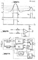
- FIG. 2 represents a conventional threshold switching circuit capable of receiving the analog signal of FIG. 1 and transforming it into one of the two pulses with steep edges Vb or Vh.
- This switching circuit consists of a differential amplifier 11 with very large gain in open loop, very conventionally connected to the resistors R 1 , R 2 , R 3 and R 4 .
- the analog signal is applied to the input E at the free terminal of the resistor R l and a reference voltage (of value h or b depending on whether the switching circuit is set on the high; or low threshold) is permanently applied at the Ref input, at the free terminal of the resistor R 2 .
- the Vb or Vh pulse is available at output S 0 .
- the differential amplifier 11 Given its significant gain, the differential amplifier 11 is always in its blocked state or in its saturated state, depending on whether the value of the analog signal is greater or less than the value of the threshold h or b chosen and applied to the input. Ref. It will be noted that given the form of the analog signal (or more exactly of its usable positive central part) the lower the chosen threshold, the longer the duration of the resulting steep edge pulse.
- a chain of recognition associated with the low threshold is necessarily the corresponding switching circuit provides "wide" pulses more easily processed by the digital logic circuits which make up the character recognition chain connected to this switching circuit.
- the digital logic circuits which make up the character recognition chain connected to this switching circuit.
- Figure 3 illustrates the system in its most general principle.
- a read head 12 has an analog signal output 13 connected to the two inputs EOb and EOh of the two threshold switching circuits SEb and SEh respective of the analog-digital conversion circuit C; the circuit SEb being adjusted with the low threshold and the circuit SEh being adjusted with the high threshold, according to the above.
- the respective outputs of these circuits SEb and SEh will be called Sb and Sh.
- the system of FIG. 3 imperatively includes a pulse signal output for each predetermined length of the character coding.
- n 2
- the internal arrangement of the recognition circuit 14 depends, of course, on the reading principle adopted, which can be, among other things, one of the three reading modes which have been briefly described above.
- the multiplexer MX is arranged to selectively correspond to the outputs SL, SC, either the inputs Ebl, Ebc, connected to the recognition chain REb (associated with the lowest threshold) or the inputs Ehl, Ehc connected to the recognition chain REh (associated with the the highest threshold).
- the transition is ensured by control means reacting to a control signal generated by the ERb circuit connected to the COM input of the MX multiplexer.
- the ERb circuit determines whether the ERb circuit signals an error or not. If the ERb circuit signals an error, a control pulse is applied to the COM input which activates the means for controlling the multiplexer. The latter then matches the inputs Ehl, Ehc with the outputs SL, SC, respectively. If the ERh circuit does not detect any identification error on the recognition chain REh (case illustrated in FIG. 1), the reading is considered to be correct and everything happens as if the system had corrected itself and its error automatically. reading. On the other hand, if the error remains, the ERh circuit can be connected to a output E R to transmit a signal capable of being taken into account by a character processing and identification unit (not shown) connected downstream of the system described in FIG. 3, that is to say in fact connected to receive at least the signals appearing at the outputs SL, SC and ER.
- a character processing and identification unit not shown
- FIG. 3 is only a system for reading and not for complete identification of the characters.
- the processing and identification unit mentioned above is designed to determine which character has been read from the order in which the pulses appear at the outputs SL and SC. Thus, we recall that for the digit O, there will be successively two pulses at the output SC then two pulses at the output SL and finally two pulses at the output SC.
- Other means, not described in FIG. 3, allow said processing and identification unit to recognize the beginning and the end of reading a character (very long interval in the case of the CMC7 code).
- the processing and identification unit If a signal is transmitted to the ER output during the reading of a character, the processing and identification unit "will know” whereas an anomaly during the reading of this character could not be corrected; since the error signal was generated by the error detection circuit connected to the recognition chain REh associated with the highest threshold.
- the processing and identification unit can then be programmed to send a "non-recognition signal" of a read character, signaling the anomaly to an operator.
- the ER output can easily be deleted if it is desirable to limit the number of connections between the reading system described and the aforementioned processing and identification unit. For this, it suffices to provide forcing means F associated with the circuit ERh and connected to the multiplexer MX. This variant is illustrated by the broken lines in FIG. 3.
- the processing and identification unit is programmed to interpret the order of succession of the pulses which appear at the outputs SL and SC. It is therefore easy to complete this unit to make it interpret the simultaneity of two pulses at the outputs SL and SC as an error (because an interval read cannot be both long and short).
- the "intelligence" of the processing and identification unit could be summarized by the following Table of Truth:
- the forcing means F are activated by the circuit ERh to apply two pulses simultaneously with the outputs SL and SC, in the event of a reading error which cannot be corrected automatically, the output ER can advantageously be suppressed.
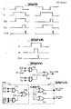
- FIG. 4 more particularly describes a reading system using a double reading head with two magneto-resistance sensors spaced apart by a distance e verifying the relationship:
- the reading system of Figure 3 operates according to the third reading mode described above.
- the first sensor or sensor A will be indifferently called the one which is arranged to read the first the presence of a magnetized segment during the useful relative movement between the read head and the document, and the second sensor or sensor B l 'other sensor reading the same information as sensor A but shifted in time because of the spacing e (400 ⁇ m in the case of code CMC7) between the two sensors.
- circuit elements receiving signals from the first sensor will carry the letter-index:: A in their reference while the circuit elements receiving signals from the second sensor will carry the letter-index B in their reference (just as we previously indicated a correlation of a circuit with a high or low threshold by an index letter h or b, respectively).
- the system of FIG. 4 will comprise two analog-digital conversion circuits Cb and Ch each comprising two threshold switching circuits.
- the circuits SEAb, SEBb which are connected to the inputs EAb, EBb of the recognition chain REb associated with the low threshold and the circuits SEAh, SEBh which are connected to the inputs EAh, EBh of the recognition chain REh associated with the high threshold .
- the analog signal output SA of sensor A is connected to inputs EOAb and EOAh of circuits SEAb and SEAh while the analog signal output SB of sensor B is connected to inputs EOBb and EO Bh of circuits SEBb and SEBh.
- the recognition chain REb has two inputs EAb and EBb connected respectively to the outputs SAb and SBb of the SEAb and SEBb circuits.
- the recognition chain REh comprises two inputs EAh and EBh connected respectively to the outputs SAh and SBh of the circuits SEAh and SEBh.
- the recognition chain REb first comprises a "means forming a monostable sensitive to a rising edge” MObl, that is to say arranged to be activated on each rising edge of its input signal and a “means forming a monostable sensitive to a falling edge "MOb2, that is to say arranged to be activated at each falling edge of its input signal.
- MObl a monostable sensitive to a rising edge
- MOb2 a monostable sensitive to a falling edge
- the monostable MObl will provide a significant output signal for each rising edge of each pulse generated by the circuit SEAb while the monostable MOb2 will provide a significant output signal for each falling edge of each pulse generated by the circuit SEAb.
- the output of the monostable MObl is connected to an input of a first combinative circuit Cbl, another input of which is connected to the input EBb (to receive the signal generated by the circuit SEBb).
- the output of the monostable MOb2 is connected to an input of a second combinational circuit Cb2, another input of which is connected to the input EBb.
- “Combinatorial circuit” means any logic gate or gate circuit arranged to produce the logic product ("as opposed to the logic sum") of the input signals.
- each combinational circuit has been symbolized by an AND gate (but one could also use a NAND gate).
- the combinational circuit Cbl is arranged to provide a significant output signal when a signal from the first monostable means MObl occurs during the duration of a pulse generated by the threshold switching circuit SEBb, associated with the sensor B.
- the combinational circuit Cb2 is arranged to supply a significant output signal when a signal from the second monostable means MOb2 occurs during the duration of a pulse generated by the threshold switching circuit SEBb.
- the outputs of the combinative circuits Cbl and Cb2 are respectively connected to the inputs of a first and of a second means forming memory JKbl and JKbc (since in practice they can be simple flip-flops JK) so that said "signals of significant outputs "of the circuits Cbl and Cb2 are immediately memorized and appear at the outputs Sbl and Sbc connected respectively to the outputs of the memories JKbl and JKbc.
- a shift register RDAb is used, the signal input of which is connected to the input EAb (to receive the pulses generated by the low threshold switching circuit SEAb connected to the first sensor A).
- An input H of the shift register receives a clock signal with relatively frequency high.
- the register also comprises a certain number of outputs sl, s2, s3, s4.
- a pulse applied to the input EAb will be transmitted to the output sl with a delay 1H (delay of a clock pulse), at the output s2 with a delay 2H, at the output s3 with a delay 3H ...
- the output sl is connected to an input of an AND gate with two inputs, Gl (or a NAND gate with two inputs) and the output s2 is connected to the second input of this same door through a NO door, G2.
- the signal available at the output sl conforms to the logic condition:
- FIG. 5a It can be seen in FIG. 5a that it is a pulse of duration 1H coinciding substantially in time with the rising edge of the signal applied to the input EAb.
- a “monostable sensitive to the rising edge” function has therefore been achieved since an output of a fixed duration pulse of value 1H (monostable) coinciding with the rising edge of the input signal is obtained at the output.
- the additional AND gate is G3 and its output is S2.
- the additional NON gate is G4; its input is connected to the output sl and its output to an input of the gate G3.
- the other input of gate G3 is directly connected to output S2.
- FIG. 8 shows an additional shift register RDBb which can be interconnected between the input EBb and said third inputs of the gates G'l, G'3 to delay the signal coming from the sensor B by a value of 1H.
- said third inputs of the doors G'1 and G'3 are connected to the output s'1 of the shift register.
- This shift register can also be usefully used to generate synchronization and reset signals for the entire system.
- the output ECH that is to say the output of the gate G5
- G5 can constitute an output of the reading system according to the invention, in the same way as the outputs SL and SC, if the processing unit and d he identification mentioned above is designed to receive the corresponding signals so as to take into account the signals transmitted to the outputs SL and / or SC only at the moment when a pulse is transmitted to the output ECH.
- the reset signal is obtained thanks to an AND gate G7 (or a NAND gate) of which an input is connected to the output s'3 via a gate NON G3 and the other input of which is directly connected to output s'4 of the shift register RDBb.
- G7 or a NAND gate
- each flip-flop JKbl, JKbc, JKhl, JKhc has a reset input (not shown) connected to the reset output of FIG. 8.
- the first type of error is equivalent to detecting the logical condition: Sbl. Sbc on the recognition chain REb associated with the low threshold or the logic condition Shl. Shc on the REh recognition chain associated with the high threshold.
- the second case is equivalent to the logical condition Sbl.S Ab for the recognition chain REb or to the condition Sbh.SAh for the recognition chain REh.
- the ERb error detection circuit could for example conform to the diagram in FIG. 11.
- An AND gate (or a NAND gate) G10 at one of its inputs connected to a complemented output Sbl of the Sbl output and its other input to the sl output (that is to say, to the delayed SAb output of 1H) while another door of the same type, Gll, has its two inputs connected to the two outputs Sbl and Sbc of the recognition chain REb.
- the outputs of these gates are connected to the two inputs of a G12 gate of the OR type or of the NON-OR type, the output of which is connected to the COM input of the MX multiplexer.
- Another type of error which is more particularly interesting to take into account when it persists on the recognition chain REh, corresponds to the case where none of the flip-flops JKhl and JKhc changed state at the end of the signal generated by the SEbh circuit (that is to say at the moment when a pulse appears at the output ECH, which normally would mean the reading of a very long interval) but that during this time a signal is actually present at the SAb output (or at the sl output of the shift register RDAb) which can only be an error.
- the processing and identification unit does not interpret the signals transmitted to it as an "end of character" when it is indeed a reading error
- the ERh circuit is designed to detect the condition:
- FIG. 12 shows a possible embodiment of the error detection circuit ERh associated with means forcing F.
- the AND gate (or a NAND gate) G13 plays exactly the same detection role as the gate G10 in FIG. 11.
- the AND gate (or NON-AND) G14 has three inputs, two of which are connected to complementary outputs (Shl and Shc) of the outputs of the recognition chain REh and whose third input is connected to the output SAb of the circuit SEAb consequently receiving signals from the sensor A.
- the outputs of the doors G13 and G14 are respectively connected to the two inputs of an OR gate (or a NOR gate) G15 and the output of this gate in fact constitutes the signal output of the ERh circuit.
- the forcing circuit F is itself made up of two OR gates (or NOR gates) G16, G17 with two inputs, two respective inputs of which are connected to the output of the ERh circuit and the other two inputs of which are respectively connected to the signal outputs from the REh recognition chain.
- the outputs of doors G16 and G17 are connected respectively to the inputs Ehl and Ehc of the MX multiplexer. If we refer to FIG. 3, we therefore see that the embodiment of the forcing circuit F represented in FIG. 12 is in fact intended to be interconnected between the outputs of the recognition chain REh and the inputs Ehc, Ehl of the multiplexer MX.
- the forcing circuit F controlled by the circuit ERh will act on the multiplexer MX to transmit signals simultaneously to the two outputs SL and SC which will be interpreted as an error by the processing and recognition unit.
Landscapes
- Engineering & Computer Science (AREA)
- Physics & Mathematics (AREA)
- General Physics & Mathematics (AREA)
- Multimedia (AREA)
- Theoretical Computer Science (AREA)
- Computer Vision & Pattern Recognition (AREA)
- Quality & Reliability (AREA)
- Character Discrimination (AREA)
- Character Input (AREA)
Applications Claiming Priority (2)
| Application Number | Priority Date | Filing Date | Title |
|---|---|---|---|
| FR7829848A FR2439433A1 (fr) | 1978-10-19 | 1978-10-19 | Systeme de lecture de caracteres |
| FR7829848 | 1978-10-19 |
Publications (2)
| Publication Number | Publication Date |
|---|---|
| EP0010495A1 true EP0010495A1 (de) | 1980-04-30 |
| EP0010495B1 EP0010495B1 (de) | 1981-12-30 |
Family
ID=9213946
Family Applications (1)
| Application Number | Title | Priority Date | Filing Date |
|---|---|---|---|
| EP79400749A Expired EP0010495B1 (de) | 1978-10-19 | 1979-10-15 | Vorrichtung zur Fehlerverbesserung in einem Erkennungssystem für kodierte Zeichen |
Country Status (7)
| Country | Link |
|---|---|
| US (1) | US4246473A (de) |
| EP (1) | EP0010495B1 (de) |
| JP (1) | JPS5556282A (de) |
| BR (1) | BR7906741A (de) |
| DE (1) | DE2961711D1 (de) |
| ES (1) | ES485207A1 (de) |
| FR (1) | FR2439433A1 (de) |
Cited By (1)
| Publication number | Priority date | Publication date | Assignee | Title |
|---|---|---|---|---|
| CN1068675C (zh) * | 1995-06-30 | 2001-07-18 | 西亚国际阿特拉斯公司 | 有形装药的钨增强衬 |
Families Citing this family (4)
| Publication number | Priority date | Publication date | Assignee | Title |
|---|---|---|---|---|
| JPH07101429B2 (ja) * | 1989-05-30 | 1995-11-01 | 富士通株式会社 | バーコードリーダーのアナログ信号処理方式 |
| US5633486A (en) * | 1995-05-19 | 1997-05-27 | Eastman Kodak Company | Apparatus for sensing magnetic fields from a wide range of magnetic media |
| US6928183B2 (en) * | 2001-09-10 | 2005-08-09 | Axiohm Transaction Solutions, Inc. | System for and method of reading MICR using high and low gain signals |
| KR101466694B1 (ko) * | 2007-08-28 | 2014-11-28 | 삼성전자주식회사 | Ecc 회로, ecc 회로를 구비하는 메모리 시스템 및그의 오류 정정 방법 |
Citations (6)
| Publication number | Priority date | Publication date | Assignee | Title |
|---|---|---|---|---|
| FR1295497A (fr) * | 1961-04-26 | 1962-06-08 | Bull Sa Machines | Perfectionnements aux systèmes d'identification de caractères |
| US3104372A (en) * | 1961-02-02 | 1963-09-17 | Rabinow Engineering Co Inc | Multilevel quantizing for character readers |
| DE1774642A1 (de) * | 1968-08-02 | 1971-10-21 | Siemens Ag | Verfahren zum Feststellen von Falschablesungen maschinell zu erkennender Schriftzeichen |
| US3764978A (en) * | 1972-05-02 | 1973-10-09 | Optical Recognition Systems | Combined magnetic optical character reader |
| US3879707A (en) * | 1972-12-20 | 1975-04-22 | Ibm | Character recognition system for bar coded characters |
| US3895350A (en) * | 1970-03-26 | 1975-07-15 | Philips Corp | Method of and device for recognition of characters |
Family Cites Families (5)
| Publication number | Priority date | Publication date | Assignee | Title |
|---|---|---|---|---|
| BE634806A (de) | 1960-07-01 | |||
| NL127547C (de) * | 1960-07-26 | |||
| US3700858A (en) * | 1971-02-24 | 1972-10-24 | Pitney Bowes Alpex | Data processing system employing particular bar code configuration |
| US3832529A (en) * | 1973-05-07 | 1974-08-27 | Seiwa Seikosha Kk | Reading system for tags encoded with bars of different widths |
| FR2402252A1 (fr) * | 1977-08-30 | 1979-03-30 | Cii Honeywell Bull | Dispositif de lecture de caracteres imprimes |
-
1978
- 1978-10-19 FR FR7829848A patent/FR2439433A1/fr active Granted
-
1979
- 1979-09-27 US US06/079,363 patent/US4246473A/en not_active Expired - Lifetime
- 1979-10-11 JP JP13007879A patent/JPS5556282A/ja active Pending
- 1979-10-15 EP EP79400749A patent/EP0010495B1/de not_active Expired
- 1979-10-15 DE DE7979400749T patent/DE2961711D1/de not_active Expired
- 1979-10-18 BR BR7906741A patent/BR7906741A/pt not_active IP Right Cessation
- 1979-10-19 ES ES485207A patent/ES485207A1/es not_active Expired
Patent Citations (6)
| Publication number | Priority date | Publication date | Assignee | Title |
|---|---|---|---|---|
| US3104372A (en) * | 1961-02-02 | 1963-09-17 | Rabinow Engineering Co Inc | Multilevel quantizing for character readers |
| FR1295497A (fr) * | 1961-04-26 | 1962-06-08 | Bull Sa Machines | Perfectionnements aux systèmes d'identification de caractères |
| DE1774642A1 (de) * | 1968-08-02 | 1971-10-21 | Siemens Ag | Verfahren zum Feststellen von Falschablesungen maschinell zu erkennender Schriftzeichen |
| US3895350A (en) * | 1970-03-26 | 1975-07-15 | Philips Corp | Method of and device for recognition of characters |
| US3764978A (en) * | 1972-05-02 | 1973-10-09 | Optical Recognition Systems | Combined magnetic optical character reader |
| US3879707A (en) * | 1972-12-20 | 1975-04-22 | Ibm | Character recognition system for bar coded characters |
Non-Patent Citations (1)
| Title |
|---|
| IBM TECHNICAL DISCLOSURE BULLETIN, Vol. 20, No. 8, Janvier 1978, Armonk (US) N. STAELBERG "Dynamic Decoding and Error Recovery System", pages 3316-3317. * Page 3317; 2 derniers alineas * * |
Cited By (1)
| Publication number | Priority date | Publication date | Assignee | Title |
|---|---|---|---|---|
| CN1068675C (zh) * | 1995-06-30 | 2001-07-18 | 西亚国际阿特拉斯公司 | 有形装药的钨增强衬 |
Also Published As
| Publication number | Publication date |
|---|---|
| BR7906741A (pt) | 1980-06-17 |
| FR2439433A1 (fr) | 1980-05-16 |
| FR2439433B1 (de) | 1984-01-06 |
| DE2961711D1 (en) | 1982-02-18 |
| ES485207A1 (es) | 1980-06-16 |
| US4246473A (en) | 1981-01-20 |
| JPS5556282A (en) | 1980-04-24 |
| EP0010495B1 (de) | 1981-12-30 |
Similar Documents
| Publication | Publication Date | Title |
|---|---|---|
| NO301392B1 (no) | Magnetisk kodeleser med innstillbare terskler | |
| EP0202251A1 (de) | Strichkodedatenträger und abtast- und dekodierapparat | |
| FR2509890A1 (fr) | Appareil de lecture de donnees pour la transmission de donnees | |
| EP0010495A1 (de) | Vorrichtung zur Fehlerverbesserung in einem Erkennungssystem für kodierte Zeichen | |
| FR2521326A1 (fr) | Appareil d'identification de code | |
| EP0011534B1 (de) | Verfahren und Vorrichtung zur Verarbeitung von analogischen, insbesondere pseudoperiodischen Signalen | |
| FR2699723A1 (fr) | Support d'enregistrement d'informations, enregistreur, lecteur et procédé d'enregistrement. | |
| EP0512925B1 (de) | Verfahren zum Kodieren eines Sicherheitsdrahtes, insbesondere für Bankpapier | |
| FR2525003A1 (fr) | Procede de lecture d'un texte imprime par une tete aiguille et tete de lecture pour la mise en oeuvre du procede | |
| EP0384536A1 (de) | Verfahren und Anordnung für die Bitsynchronisation in einem digitalen Datenempfänger | |
| EP1554810B1 (de) | Optischer winkelcodierer | |
| EP0029923A1 (de) | Schaltkreis zur Steuerung eines Pufferspeichers | |
| EP0695979B1 (de) | Vorrichtung zum Erkennen eines auf einer Oberfläche geschriebenen Buchstaben und Verfahren zum Erkennen eines solchen Buchstaben, insbesondere für eine Uhr | |
| EP1131772B1 (de) | Verfahren zur digitalen übertragung | |
| FR2548801A2 (fr) | Carte a lecture optique portant des informations numeriques et systeme de controle d'acces a des informations diffusees utilisant une telle carte | |
| FR2480007A1 (fr) | Systeme optique de lecture de caracteres | |
| EP0905946A1 (de) | Reglung der Abtastung von Biphasensignale | |
| EP0192595A1 (de) | Verfahren und Anordnung zur Übertragung von kodierten Daten | |
| EP0390649A1 (de) | Vorrichtung und Verfahren zur Erkennung der augenblicklichen Stellung von von einem Schrittmotor angetriebenen mechanischen Teilen | |
| FR2459591A1 (fr) | Procede et dispositif de telecopie a sauts de blancs | |
| EP0206900B1 (de) | Lesegerät für optischen Kode, insbesondere eines völlig integrierten Typs | |
| EP1393450B1 (de) | Einrichtung zum empfangen digitaler signale | |
| EP1196914B1 (de) | Spurfolgesystem zur aufzeichnung/wiedergabe eines informationsträgers und aufzeichnungsträger | |
| EP0540397B1 (de) | Anordnung und Verfahren zum Zählen von Taktschlupfen | |
| FR2767218A1 (fr) | Code magnetique comportant une base de lecture et systeme de lecture d'un tel code |
Legal Events
| Date | Code | Title | Description |
|---|---|---|---|
| PUAI | Public reference made under article 153(3) epc to a published international application that has entered the european phase |
Free format text: ORIGINAL CODE: 0009012 |
|
| AK | Designated contracting states |
Designated state(s): DE GB IT NL |
|
| 17P | Request for examination filed | ||
| ITF | It: translation for a ep patent filed | ||
| GRAA | (expected) grant |
Free format text: ORIGINAL CODE: 0009210 |
|
| AK | Designated contracting states |
Designated state(s): DE GB IT NL |
|
| REF | Corresponds to: |
Ref document number: 2961711 Country of ref document: DE Date of ref document: 19820218 |
|
| ITTA | It: last paid annual fee | ||
| PGFP | Annual fee paid to national office [announced via postgrant information from national office to epo] |
Ref country code: GB Payment date: 19961001 Year of fee payment: 18 |
|
| PGFP | Annual fee paid to national office [announced via postgrant information from national office to epo] |
Ref country code: NL Payment date: 19961031 Year of fee payment: 18 |
|
| PGFP | Annual fee paid to national office [announced via postgrant information from national office to epo] |
Ref country code: DE Payment date: 19961114 Year of fee payment: 18 |
|
| PG25 | Lapsed in a contracting state [announced via postgrant information from national office to epo] |
Ref country code: GB Free format text: LAPSE BECAUSE OF NON-PAYMENT OF DUE FEES Effective date: 19971015 |
|
| PG25 | Lapsed in a contracting state [announced via postgrant information from national office to epo] |
Ref country code: NL Free format text: LAPSE BECAUSE OF NON-PAYMENT OF DUE FEES Effective date: 19980501 |
|
| GBPC | Gb: european patent ceased through non-payment of renewal fee |
Effective date: 19971015 |
|
| NLV4 | Nl: lapsed or anulled due to non-payment of the annual fee |
Effective date: 19980501 |
|
| PG25 | Lapsed in a contracting state [announced via postgrant information from national office to epo] |
Ref country code: DE Free format text: LAPSE BECAUSE OF NON-PAYMENT OF DUE FEES Effective date: 19980701 |
|
| PLBE | No opposition filed within time limit |
Free format text: ORIGINAL CODE: 0009261 |
|
| STAA | Information on the status of an ep patent application or granted ep patent |
Free format text: STATUS: NO OPPOSITION FILED WITHIN TIME LIMIT |