EP0006002B1 - Method of fabricating a field effect transistor - Google Patents
Method of fabricating a field effect transistor Download PDFInfo
- Publication number
- EP0006002B1 EP0006002B1 EP79300998A EP79300998A EP0006002B1 EP 0006002 B1 EP0006002 B1 EP 0006002B1 EP 79300998 A EP79300998 A EP 79300998A EP 79300998 A EP79300998 A EP 79300998A EP 0006002 B1 EP0006002 B1 EP 0006002B1
- Authority
- EP
- European Patent Office
- Prior art keywords
- substrate
- active layer
- layer
- gate electrode
- mesa
- Prior art date
- Legal status (The legal status is an assumption and is not a legal conclusion. Google has not performed a legal analysis and makes no representation as to the accuracy of the status listed.)
- Expired
Links
Images


Classifications
-
- H—ELECTRICITY
- H10—SEMICONDUCTOR DEVICES; ELECTRIC SOLID-STATE DEVICES NOT OTHERWISE PROVIDED FOR
- H10D—INORGANIC ELECTRIC SEMICONDUCTOR DEVICES
- H10D30/00—Field-effect transistors [FET]
- H10D30/80—FETs having rectifying junction gate electrodes
- H10D30/87—FETs having Schottky gate electrodes, e.g. metal-semiconductor FETs [MESFET]
- H10D30/875—FETs having Schottky gate electrodes, e.g. metal-semiconductor FETs [MESFET] having thin-film semiconductor bodies
-
- H—ELECTRICITY
- H10—SEMICONDUCTOR DEVICES; ELECTRIC SOLID-STATE DEVICES NOT OTHERWISE PROVIDED FOR
- H10D—INORGANIC ELECTRIC SEMICONDUCTOR DEVICES
- H10D30/00—Field-effect transistors [FET]
- H10D30/80—FETs having rectifying junction gate electrodes
- H10D30/87—FETs having Schottky gate electrodes, e.g. metal-semiconductor FETs [MESFET]
-
- H—ELECTRICITY
- H10—SEMICONDUCTOR DEVICES; ELECTRIC SOLID-STATE DEVICES NOT OTHERWISE PROVIDED FOR
- H10D—INORGANIC ELECTRIC SEMICONDUCTOR DEVICES
- H10D64/00—Electrodes of devices having potential barriers
- H10D64/20—Electrodes characterised by their shapes, relative sizes or dispositions
- H10D64/23—Electrodes carrying the current to be rectified, amplified, oscillated or switched, e.g. sources, drains, anodes or cathodes
- H10D64/251—Source or drain electrodes for field-effect devices
-
- H—ELECTRICITY
- H10—SEMICONDUCTOR DEVICES; ELECTRIC SOLID-STATE DEVICES NOT OTHERWISE PROVIDED FOR
- H10D—INORGANIC ELECTRIC SEMICONDUCTOR DEVICES
- H10D64/00—Electrodes of devices having potential barriers
- H10D64/20—Electrodes characterised by their shapes, relative sizes or dispositions
- H10D64/27—Electrodes not carrying the current to be rectified, amplified, oscillated or switched, e.g. gates
- H10D64/311—Gate electrodes for field-effect devices
- H10D64/411—Gate electrodes for field-effect devices for FETs
-
- H—ELECTRICITY
- H10—SEMICONDUCTOR DEVICES; ELECTRIC SOLID-STATE DEVICES NOT OTHERWISE PROVIDED FOR
- H10P—GENERIC PROCESSES OR APPARATUS FOR THE MANUFACTURE OR TREATMENT OF DEVICES COVERED BY CLASS H10
- H10P50/00—Etching of wafers, substrates or parts of devices
- H10P50/60—Wet etching
- H10P50/64—Wet etching of semiconductor materials
- H10P50/642—Chemical etching
- H10P50/646—Chemical etching of Group III-V materials
-
- H—ELECTRICITY
- H10—SEMICONDUCTOR DEVICES; ELECTRIC SOLID-STATE DEVICES NOT OTHERWISE PROVIDED FOR
- H10W—GENERIC PACKAGES, INTERCONNECTIONS, CONNECTORS OR OTHER CONSTRUCTIONAL DETAILS OF DEVICES COVERED BY CLASS H10
- H10W20/00—Interconnections in chips, wafers or substrates
- H10W20/40—Interconnections external to wafers or substrates, e.g. back-end-of-line [BEOL] metallisations or vias connecting to gate electrodes
-
- H—ELECTRICITY
- H10—SEMICONDUCTOR DEVICES; ELECTRIC SOLID-STATE DEVICES NOT OTHERWISE PROVIDED FOR
- H10W—GENERIC PACKAGES, INTERCONNECTIONS, CONNECTORS OR OTHER CONSTRUCTIONAL DETAILS OF DEVICES COVERED BY CLASS H10
- H10W72/00—Interconnections or connectors in packages
- H10W72/30—Die-attach connectors
-
- H—ELECTRICITY
- H10—SEMICONDUCTOR DEVICES; ELECTRIC SOLID-STATE DEVICES NOT OTHERWISE PROVIDED FOR
- H10W—GENERIC PACKAGES, INTERCONNECTIONS, CONNECTORS OR OTHER CONSTRUCTIONAL DETAILS OF DEVICES COVERED BY CLASS H10
- H10W72/00—Interconnections or connectors in packages
- H10W72/071—Connecting or disconnecting
- H10W72/073—Connecting or disconnecting of die-attach connectors
-
- H—ELECTRICITY
- H10—SEMICONDUCTOR DEVICES; ELECTRIC SOLID-STATE DEVICES NOT OTHERWISE PROVIDED FOR
- H10W—GENERIC PACKAGES, INTERCONNECTIONS, CONNECTORS OR OTHER CONSTRUCTIONAL DETAILS OF DEVICES COVERED BY CLASS H10
- H10W72/00—Interconnections or connectors in packages
- H10W72/071—Connecting or disconnecting
- H10W72/073—Connecting or disconnecting of die-attach connectors
- H10W72/07331—Connecting techniques
- H10W72/07337—Connecting techniques using a polymer adhesive, e.g. an adhesive based on silicone or epoxy
-
- Y—GENERAL TAGGING OF NEW TECHNOLOGICAL DEVELOPMENTS; GENERAL TAGGING OF CROSS-SECTIONAL TECHNOLOGIES SPANNING OVER SEVERAL SECTIONS OF THE IPC; TECHNICAL SUBJECTS COVERED BY FORMER USPC CROSS-REFERENCE ART COLLECTIONS [XRACs] AND DIGESTS
- Y10—TECHNICAL SUBJECTS COVERED BY FORMER USPC
- Y10S—TECHNICAL SUBJECTS COVERED BY FORMER USPC CROSS-REFERENCE ART COLLECTIONS [XRACs] AND DIGESTS
- Y10S438/00—Semiconductor device manufacturing: process
- Y10S438/977—Thinning or removal of substrate
Definitions
- This invention relates to a method of fabricating field-effect transistors (FETs) according to the first part of claim 1.
- Conventional low-noise microwave FETs normally comprise a high resistivity or semi-insulating semiconductor substrate formed with a thin high-quality epitaxial active layer on which the source, gate and drain electrodes are formed.
- the described method involves formation of ohmic source and drain electrodes on the surface of an epitaxial active layer formed on a semiconductor substrate; sealing this surface to a dielectric support substrate; removing the original semiconductor substrate using differential etching; and then forming a gate electrode on the surface of the active layer opposite to that on which the source and drain electrodes are formed.
- a method according to the first part of claim 1 is therefore known from the US Government Reports Announcements, Vol. 77, No. 5, December 19, 1975, pages 1-6 and 26-28. From the US-A-3972770 it is known to etch a layer of GaAs on a supporting layer of GaAIAs in an etchant solution which is formed of equal volumes of a 30% solution of hydrogen peroxide, and a 28% solution of ammonium hydroxide with the balance being water. From DE-A-1514943 a semiconductor device is known the electrodes of which have a portion which extends continuously over the edge of a semiconductor mesa to provide a contact pad for external connection to the device.
- a method of fabricating a field effect transistor comprises the steps of forming an active layer of semiconductor material over a surface of a first substrate of semiconductor material, applying a second substrate of insulating material to the surface of the structure comprising the first substrate and active layer so that the active layer lies between the two substrates, removing the first substrate, and forming a gate electrode over the surface of the active layer opposite the second substrate, characterised in that a buffer layer of semiconductor material is formed on the surface of the first substrate prior to formation of the active layer and is removed following removal of the first substrate and that, together with the gate electrode, source and drain electrodes are formed over the surface of the active layer opposite the second substrate.
- FET field effect transistor
- the method in accordance with the invention can be used to make coplanar FETs (i.e. in which the source, drain and gate electrodes all lie on the same side of the active layer) of substantially conventional design except that the usual high resistivity or semi-insulating semiconductor substrate is replaced by a substrate having good insulating properties.
- coplanar FETs i.e. in which the source, drain and gate electrodes all lie on the same side of the active layer
- design and fabrication procedures similar to those used for conventional FETs may be used to complete the device fabrication.
- the first substrate is removed by etching using a selective etchant which attacks it faster than it attacks the buffer layer
- the buffer layer may then also be removed by etching using a selective etchant which attacks it at a faster rate than it attacks the first substrate.
- a very thin and even active layer is obtained.
- a barrier against migration of impurities from the conventionally low purity temporary substrate to the active layer is provided. A high quality active layer may therefore be obtained.
- the buffer layer preferably comprises GaAIAs removed using HF as the etchant.
- a thin surface layer of the active layer at least in the region on which the gate electrode is to be formed may be removed prior to formation of the gate electrode to remove any impurities or surface defects in the active layer due to its interface with other layers.
- a thin layer of high conductivity semiconductor material of the same conductivity type as the active layer is formed immediately prior to the formation of the active layer on its surface, and following removal of the first substrate and buffer layer, the source and drain electrodes are then formed as ohmic contacts on this high conductivity layer. This improves the quality of the ohmic contacts. Part of this high conductivity layer between the source and drain contacts is removed, preferably after the source and drain electrodes are formed to enable the gate electrode to be applied as a Schottky barrier contact with the active layer.
- This air gap may conveniently be achieved by recessing the surface of the active layer, on which the gate electrode is to be formed before applying the second substrate.
- a non-conducting semiconductor layer may be formed on the free surface of the active layer, and a region of this non-conducting layer then etched away to expose the channel region of the active layer immediately opposite that on which the gate electrode is to be formed.
- the second substrate may be of any suitable insulating material.
- the material used and/or its bond with the structure comprising the first substrate, buffer layer and active layer should have good mechanical properties, provide a good thermal expansion match with the active layer and first substrate, and be capable of withstanding the temperatures and chemicals used in subsequent fabrication steps.
- the second substrate or at least the means by which it is applied to the first substrate, buffer layer and active layer structure should also have good microwave properties.
- the process used to apply the second substrate to the structure comprising the first substrate, buffer layer and active layer must cause no substantial degradation of the active layer, particularly in the gate region.
- the second substrate may be applied by means of a suitable adhesive, e.g. polyimide.
- a suitable adhesive e.g. polyimide.
- a suitable polyimide adhesive is Kerimid (Registered Trade Mark) 601, a polyimide resin manufactured by Rhone-Poulenc, which combines good microwave properties with good chemical and thermal stability.
- a coating of suitable insulating material such as Si0 2 , Si 3 N 4 , Alumina, a plastics, e.g. polyimide glass or polycrystalline GaAs may be applied to the appropriate surface of the structure comprising the first substrate, buffer layer, and the active layer, and the second substrate then bonded to this insulating coating using a suitable adhesive.
- suitable adhesive e.g. polyimide glass or polycrystalline GaAs
- a further method of applying the second substrate is to form it in situ on the surface of the structure comprising the first substrate, buffer layer and active layer, or on the insulating coating where provided.
- the second substrate may comprise glass applied to the structure comprising the first substrate, buffer layer and active layer by first applying a coating of Si0 2 and then fusion bonding the glass substrate to the Si0 2 coating.
- Any suitably low melting point glass, such as borosilicate glass, may be used instead of SiO 2 .
- a low noise microwave FET is fabricated in accordance with the invention by forming a buffer layer 1 of GaAIAs having a thickness of the order of 2 to 5 ⁇ m, on a first substrate 2 of semi-insulating GaAs, typically about 200 pm thick, and then forming a thin (0.2 to 0.5 ⁇ m) layer 4 of high conductivity (n + ) GaAs followed by an active layer 5 of n-type GaAs in the range 0.2 to 1 pm thick, on the surface of the buffer layer 1.
- Each of the layers is grown by liquid or vapour phase, or molecular beam epitaxy in accordance with known techniques.
- the structure comprising the substrate 2, buffer layer 1, high conductivity layer 4 and active layer 5 is then bonded to a second, glass substrate 6, of the order of 2 mm thick. This is effected by coating the free surface of the active layer 5 with a layer 7 of Si0 2 applied by chemical vapour deposition to a thickness of the order of 0.2 ,um, to which the second substrate 6 is heat bonded at a temperature of about 700°C.
- a suitable glass for the second substrate is Corning (Registered Trade Mark) glass 7056.
- the rear surface of the glass may at this stage be lapped down to a thickness of about 0.4 mm and polished. Slots 8 are then cut into the rear surface at device pitch and parallel to the cleavage planes. Alternatively these slots may be cut into the top surface of the glass substrate 6 before it is bonded to the active layer 5.
- the first substrate 2 is then removed using a selective etchant comprising a 95:5 mixture of 100V H 2 0 2 and 35% NH 4 0H which attacks GaAs at a faster rate than it attacks GaAIAs.
- the GaAIAs buffer layer 1 thus acts as a chemical stop to the etchant used to remove the GaAs substrate 2, so that the etching process stops at the GaAs/GaAIAs interface.
- the GaAIAs buffer layer 1 is then removed by a different selective etchant comprising a 50% solution of HF in water, which is capable of etching GaAIAs at a much faster rate than it etches GaAs of which the underlying epitaxial layers 4, 5 are formed.
- the HF etching process can thus be made to stop exactly at the interface of the GaAIAs buffer layer 1 and the high conductivity GaAs layer 4.
- the above differential etching procedure is used to effect removal of the first GaAs substrate 2 because it is difficult, using conventional GaAs etching techniques, to etch down evenly to the required accuracy ( ⁇ 0.01 ,um) over a large area when the total etch depth is of the order of several hundred microns.
- parts of the active layer 5 and the high conductivity layer 4 are first etched away to leave a separate isolated mesa for each device on the surface of the second substrate 6.
- Ohmic source and drain contacts 9, 10 are then applied in a conventional manner by first forming a resist mask having holes where the electrode metallisations are to be applied to the surface of the structure, applying a metallisation layer over the surface of the resist mask, floating off the metallisation layer overlying the resist mask, and then annealing at a temperature of about 450°C to form an ohmic contact between the contact metallisations 9, 10 and the semiconductor mesa.
- the purpose of the high conductivity semiconductor layer 4 is to improve the quality of the ohmic contact between the source and drain electrodes 9, 10 and the active GaAs layer 5 as is known in the art.
- a groove or recess 11 is formed in the semiconductor mesa structure in the space between the opposing edges of the source and drain contacts, the groove lying parallel to these two edges and extending to a depth greater than the thickness of the high conductivity layer 4.
- the groove or recess is formed in conventional manner by applying a resist mask over the surface of the structure having a hole corresponding in shape and position to that of the required groove, and the exposed GaAs removed using a suitable etchant. The etching process is carefully controlled to leave the desired thickness of active GaAs between the floor of the groove 11 and the glass substrate 6. It is this thickness which determines the channel current of the device and will typically be of the order of 0.1 to 0.3 ⁇ m.
- the resist is then removed and the gate electrode 12 of the device then formed.
- the gate electrode 12 comprising a narrow strip of conductor extending centrally along the floor of the groove 11 and over the edge of the mesa to terminate in an enlarged contact pad on the surface of the Si0 2 layer 7 overlying the substrate 6, is again formed in conventional manner, conveniently using the same resist mask, to provide a Schottky barrier contact with the active GaAs layer between the source and drain electrodes, 9, 10.
- the glass substrate 6 is then diced up into individual device chips by cleavage along the pre-formed slots 8.
- the high conductivity GaAs layer 4 is provided to improve the quality of the ohmic contact between the source and drain electrodes 9, 10 and the active GaAs layer 5 is optional, and may be omitted altogether.
- FIG. 2 A typical completed device structure is shown in Figure 2, from which it will be seen that the etched edges of the mesa and the gate electrode recess 11 are inclined at an angle determined by the crystal orientation of the GaAs.
- the particular etchant used i.e. a 1:10.05 NaOH/5V H 2 0 2 mixture is orientation sensitive and is thus capable of producing etch grooves which have either a 'V' or 'A' (dovetail) cross-section depending on which face of the GaAs the etchant is applied to.
- the crystal orientation has been chosen to produce a groove 11 of 'A'-line or dovetail cross-section so that the edge of the mesa over which the gate electrode 12 passes onto the surface of the substrate slopes outwardly, ensuring continuity of the gate electrode.
- This also produces an increased resistance between the gate electrode 12 and the ohmic source and drain contacts 9, 10 due to the increased length of active GaAs between them across the floor of the recess 11.
- Another consequence of this orientation is that edges of the mesa over which the source and drain electrodes 9, 10 would normally pass onto the surface of the substrate are undercut.
- castellations 14, 14a are provided as shown, enabling the electrodes to pass continuously onto the substrate over outwardly sloping edges of the mesa.
- the mesa may be made larger, and the source and drain electrodes 9, 10 formed wholly on the mesa.
- a suitable alternative method of removing the GaAs to form the recesses 11 and the mesa, is ion milling. As this process is independent of the crystal orientation the above difficulties do not arise.
- an air gap may be provided between these surfaces so that the active GaAs layer is interfaced to air in the gate region. This may be achieved either by recessing the glass substrate in the immediate vicinity of the gate region before bonding it to the active layer, or preferably by suitably recessing the active layer 5 in the gate region as shown in Figure 3 before bonding it to the glass substrate.
- This recess 15 on the free surface of the active GaAs layer 5 is formed by etching using a resist mask, before application of the SiO 2 layer 7. Additionally, before the Si0 2 layer 7 is applied, alignment holes extending through the active GaAs layer 5, and the high conductivity layer 4 where provided, are formed to enable the resist mask, applied over the opposite side of the GaAs active layer to form the mesa during later stages in the fabrication, to be aligned with the recess 15.
- these holes are used to align the mesa etch mask, and the positions of subsequent resist masks used in the formation of the source, gate and drain electrodes can then be aligned with respect to the edges of the recess 15 revealed at the edge of the mesa to ensure registration of the gate electrode with the recess 15.
- a disadvantage of this particular process arises from the need to maintain continuity of the gate electrode 12 as it passes over the mesa edge, so that the recess 15 must terminate short of the mesa edge as illustrated in Figure 4.
- the distance between the termination of the recess and the edge of the mesa may occupy up to 10% of the total effective gate width (i.e. in its direction of elongation). This results in a shunt path for the device current when the remaining part of the channel is near pinch-off during operation, and hence degrades the mutual conductance characteristics of the device.
- This problem may be overcome by a further modification of the above fabrication procedure.
- alignment holes extending through the layer 16, the active layer 5, and the high conductivity layer 4 where provided, are also formed prior to formation of the Si0 2 to enable alignment of the mesa resist mask with the recess 1 8.
- the invention thus provides a low-noise microwave FET structure in which the surface of the active layer in the channel region opposite the gate electrode is interfaced either to a good insulator or to air, so ensuring that the charge carriers are confined to the active GaAs layer 5 during operation particularly near pinch-off.
- the glass substrate 6 may be applied to the structure comprising the first substrate 2 and active layer 5 using instead of Si0 2 , a low melting point glass such as borosilicate glass applied for example by sputtering or evaporation.
- a low melting point glass such as borosilicate glass applied for example by sputtering or evaporation.
- the second substrate which may be of any suitable insulating material, may be applied using an adhesive, for example a polyimide resin.
- an adhesive for example a polyimide resin.
- a polyimide resin is that sold under the name of Kerimid (Registered Trade Mark) 601 as discussed earlier used with an alumina second substrate.
- a further method of applying the insulating substrate using an adhesive involves applying a thin coating of insulating material of the order of 10 to 50 ⁇ m thick to the appropriate surface of the structure comprising the first substrate buffer layer and active layer, and then applying the second substrate to this insulating coating using an adhesive.
- the insulating coating may comprise for example Si0 2 , S I3 N 4 , Alumina, glass, polycrystalline GaAs or a plastics resin, such as polyimide applied using any suitable known technique which does not cause degradation of the active layer. Because the adhesive used need not have such good microwave properties or be such a good expansion match to the active layer and first substrate being relatively remote therefrom, a much wider range of adhesives may be used.
- a coating 20 of a suitable insulating material which for the purposes of the present example comprises a polyimide resin such as Kerimid (Registered Trade Mark) 601 is applied to the free surface of the active layer 5 in liquid form (i.e. in solution).
- the entire coated structure is then spun at high speed to produce a uniformly thick coating of the polyimide resin of the desired thickness, typically several tens of microns thick although this is not critical.
- the structure is then heated to about 120°C for 30 minutes to dry the solvent before curing the resin at a temperature of 220°C again for approximately 30 minutes.
- the result is a substantially bubble-free coating 20 having good mechanical and low-loss microwave properties, thermally and chemically compatible with the GaAs active layer 5.
- the coating 20 may be built up from a plurality of successively formed thinner (sub-micron) layers of the coating material.
- the second substrate 21, comprising a plate of glass or any other suitable insulating material, is applied to the polyimide coating 20 using a suitable adhesive 22.
- the adhesive used must of course be capable of withstanding the annealing temperature (450°) used in forming the source and drain contacts 10, 11 as well as being chemically resistant to the etchants and solvents used in the later fabrication stages.
- the low-loss coating 20 provides a mechanical barrier between the active layer and this adhesive, the requirements of the adhesive in terms of its chemical and thermal compatibility with the active layer, and its microwave properties can be considerably relaxed.
- the coating may alternatively comprise Si0 2 , S 13 N 4 , Alumina, glass, or polycrystalline GaAs applied as appropriate by evaporation, sputtering ion deposition or any other process capable of producing a high quality coating having good low-loss microwave properties.
- the substrate may then be applied to this coating as described above, using an adhesive, or it may be formed in situ by any suitable technique such as by moulding at elevated temperature and pressure.
- a second substrate of plastic material e.g. polyimide
- a second substrate of glass e.g. borosilicate glass, may be applied by evaporation or sputtering, or as a glass frit, but this latter technique involves a relatively high temperate fusion process.
- the second substrate may also be applied directly to the structure comprising the first substrate, buffer layer and active layer, using a suitable adhesive, e.g. polyimide, but the above initial coating process is preferred as this enables the material interfaced, to the active layer to be inspected for quality.
- a suitable adhesive e.g. polyimide
- the mesa may be defined before application of the second substrate. This may be achieved either by complete removal of the part of the active and high conductivity GaAs layers 5, 4 surrounding the mesa, so that the mesa is completely isolated before application of the second substrate, or by removing only part of the total thickness of the GaAs layers 4, 5 (or layer 5 where no high conductivity layer 4 is provided) before application of the second substrate, and then free etching the surface of the GaAs exposed by removal of the first substrate 2 and buffer layer, to complete removal of the reduced thickness of GaAs and thereby completely isolate the mesa.
- the mesa thus formed will be embedded in the insulating material used in applying the second substrate, and its top surface will be flush with, or be slightly recessed with respect to the surface of the insulating material.
- the source, drain and gate electrodes may thus be formed using the same procedures as before, the top surface of the mesa being recessed before formation of the gate electrode therein, without the above difficulties associated with draping the electrodes over the mesa edge.
- the first semiconductor substrate on which the active layer is formed may be removed using any suitable technique capable of effecting the removal without substantially affecting the quality or uniformity of thickness of the active layer.
- the active layer may initially be formed thicker than required, and a thin surface layer then removed following removal of the first substrate.
- a buffer layer of high quality semiconductor material mey be formed on the surface of the first substrate prior to the formation of the active layer, this buffer layer then being removed following removal of the first substrate.
- this buffer layer (GaAIAs where the substrate and active layer are GaAs) also acts as a chemical stop to the differential etchant used to remove the first substrate.
- this buffer layer also acts as a chemical stop to the differential etchant used to remove the first substrate.
- the subsequently formed device structure may be of any known configuration.
- two source-drain gaps may be provided between a pair of source electrodes and a single central drain electrode, or vice versa, with a pair of gate electrodes extending from a common connection pad into the said gaps resulting in a reduced gate resistance for a given total gate width (i.e. width in the direction of elongation along the source-drain gap).
- a power FET device comprising a plurality of such FETs connected in parallel, i.e. with their respective source, drain and gate electrodes connected together, may be formed on a common substrate.
Landscapes
- Junction Field-Effect Transistors (AREA)
- Bipolar Transistors (AREA)
- Thin Film Transistor (AREA)
Description
- This invention relates to a method of fabricating field-effect transistors (FETs) according to the first part of
claim 1. - Conventional low-noise microwave FETs normally comprise a high resistivity or semi-insulating semiconductor substrate formed with a thin high-quality epitaxial active layer on which the source, gate and drain electrodes are formed.
- Theoretical and experimental evidence suggests that the performance of conventional low-noise microwave FETs, and also to a certain extent power FETs, is limited because of a reduction in the mutual conductance (gm) of the device as the gate bias is increased towards pinch-off. It is thought that the major reason for this reduction in mutual conductance is that charge carriers in the active channel region underlying the gate electrode are forced into the substrate at a high gate biases, with a resultant 'softening' of the I-V characteristics. To enable high mutual conductance to be achieved near pinch-off, it is desirable to maintain the charge carriers within the active layer.
- It has been proposed to adapt the technology developed for the fabrication of GaAs photocathodes to the fabrication of low-noise non-coplanar GaAs FETs to enable the active channel region underlying the gate electrode to be interfaced to a good insulator instead of to the usual high resistivity of semi-insulating GaAs substrate, and to enable the gate electrode be placed on the opposite side of the active layer to the source and drain electrodes (non-coplanar). A method of fabricating such an FET is described in Annual Report No. (1976-1975) prepared by D. R. Decker and S. G. Bandy of Varian Associates, Palo Alto, California under contract No. N00014-75-C-0303 with the US Office of Naval Research, which publication is abstracted in US Government Reports Announcements Vol. 77, No. 5 field 9A under No. ADA032809.
- The described method involves formation of ohmic source and drain electrodes on the surface of an epitaxial active layer formed on a semiconductor substrate; sealing this surface to a dielectric support substrate; removing the original semiconductor substrate using differential etching; and then forming a gate electrode on the surface of the active layer opposite to that on which the source and drain electrodes are formed.
- A method according to the first part of
claim 1 is therefore known from the US Government Reports Announcements, Vol. 77, No. 5, December 19, 1975, pages 1-6 and 26-28. From the US-A-3972770 it is known to etch a layer of GaAs on a supporting layer of GaAIAs in an etchant solution which is formed of equal volumes of a 30% solution of hydrogen peroxide, and a 28% solution of ammonium hydroxide with the balance being water. From DE-A-1514943 a semiconductor device is known the electrodes of which have a portion which extends continuously over the edge of a semiconductor mesa to provide a contact pad for external connection to the device. - According to the present invention, a method of fabricating a field effect transistor (FET) comprises the steps of forming an active layer of semiconductor material over a surface of a first substrate of semiconductor material, applying a second substrate of insulating material to the surface of the structure comprising the first substrate and active layer so that the active layer lies between the two substrates, removing the first substrate, and forming a gate electrode over the surface of the active layer opposite the second substrate, characterised in that a buffer layer of semiconductor material is formed on the surface of the first substrate prior to formation of the active layer and is removed following removal of the first substrate and that, together with the gate electrode, source and drain electrodes are formed over the surface of the active layer opposite the second substrate.
- The method in accordance with the invention can be used to make coplanar FETs (i.e. in which the source, drain and gate electrodes all lie on the same side of the active layer) of substantially conventional design except that the usual high resistivity or semi-insulating semiconductor substrate is replaced by a substrate having good insulating properties. Thus, after the removal of the first substrate, design and fabrication procedures similar to those used for conventional FETs may be used to complete the device fabrication.
- Preferably the first substrate is removed by etching using a selective etchant which attacks it faster than it attacks the buffer layer, and the buffer layer may then also be removed by etching using a selective etchant which attacks it at a faster rate than it attacks the first substrate. In this way a very thin and even active layer is obtained. Additionally, by using a high quality buffer layer between this layer and the temporary substrate, a barrier against migration of impurities from the conventionally low purity temporary substrate to the active layer is provided. A high quality active layer may therefore be obtained.
- Where the first substrate comprises GaAs, and the active layer is n-type GaAs, the buffer layer preferably comprises GaAIAs removed using HF as the etchant.
- Whatever method of removing the first substrate is used, a thin surface layer of the active layer at least in the region on which the gate electrode is to be formed, may be removed prior to formation of the gate electrode to remove any impurities or surface defects in the active layer due to its interface with other layers.
- Preferably a thin layer of high conductivity semiconductor material of the same conductivity type as the active layer is formed immediately prior to the formation of the active layer on its surface, and following removal of the first substrate and buffer layer, the source and drain electrodes are then formed as ohmic contacts on this high conductivity layer. This improves the quality of the ohmic contacts. Part of this high conductivity layer between the source and drain contacts is removed, preferably after the source and drain electrodes are formed to enable the gate electrode to be applied as a Schottky barrier contact with the active layer.
- Where there is a likelihood of degradation of the active layer due to the presence of, or the techniques used in applying, the second substrate to the structure comprising the first substrate buffer layer and active layer, this problem can be alleviated by providing an air gap at the interface between the gate region of the active layer and the second substrate or its bonding medium. Any degradation of the active layer in the gate region, i.e. that region underlying the gate electrode and providing the channel of the FET, will critically affect the low noise operation of the device.
- This air gap may conveniently be achieved by recessing the surface of the active layer, on which the gate electrode is to be formed before applying the second substrate. Alternatively, prior to application of the second substrate, a non-conducting semiconductor layer may be formed on the free surface of the active layer, and a region of this non-conducting layer then etched away to expose the channel region of the active layer immediately opposite that on which the gate electrode is to be formed.
- The second substrate may be of any suitable insulating material. However, the material used and/or its bond with the structure comprising the first substrate, buffer layer and active layer should have good mechanical properties, provide a good thermal expansion match with the active layer and first substrate, and be capable of withstanding the temperatures and chemicals used in subsequent fabrication steps. Where the method is used to fabricate microwave FETs, the second substrate or at least the means by which it is applied to the first substrate, buffer layer and active layer structure, should also have good microwave properties. In addition, the process used to apply the second substrate to the structure comprising the first substrate, buffer layer and active layer must cause no substantial degradation of the active layer, particularly in the gate region.
- The second substrate may be applied by means of a suitable adhesive, e.g. polyimide. A suitable polyimide adhesive is Kerimid (Registered Trade Mark) 601, a polyimide resin manufactured by Rhone-Poulenc, which combines good microwave properties with good chemical and thermal stability.
- Alternatively, a coating of suitable insulating material such as Si02, Si3N4, Alumina, a plastics, e.g. polyimide glass or polycrystalline GaAs may be applied to the appropriate surface of the structure comprising the first substrate, buffer layer, and the active layer, and the second substrate then bonded to this insulating coating using a suitable adhesive. The requirements for this adhesive as regards its thermal expansion and chemical match to the structure, and its microwave properties are far less stringent, and so a wider range of adhesives may be used.
- A further method of applying the second substrate is to form it in situ on the surface of the structure comprising the first substrate, buffer layer and active layer, or on the insulating coating where provided.
- The second substrate may comprise glass applied to the structure comprising the first substrate, buffer layer and active layer by first applying a coating of Si02 and then fusion bonding the glass substrate to the Si02 coating. Any suitably low melting point glass, such as borosilicate glass, may be used instead of SiO2.
- The invention will now be described in more detail, by way of example only, with reference to the accompanying drawings, in which:
- Figures 1 (a) to 1 (d) show schematic sectional views illustrating various stages in the fabrication of a FET by a method in accordance with the present invention;
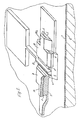
- Figure 2 is a diagrammatic part-sectional, perspective view of an FET fabricated by the method illustrated in Figure 1;
- Figure 3 is a schematic perspective part-sectional view of a modified form in accordance with the invention;
- Figure 4 is a diagrammatic part-sectional perspective view of part of the device shown in Figure 3;
- Figure 5 is a diagrammatic part-sectional perspective view of part of a further modified form of FET in accordance with the invention; and
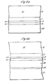
- Figures 6(a) and 6(b) show schematic sectional views illustrating various stages in a modified method of fabricating a FET in accordance with the invention.
- Referring to Figures 1 (a) to 1 (d) a low noise microwave FET is fabricated in accordance with the invention by forming a
buffer layer 1 of GaAIAs having a thickness of the order of 2 to 5 µm, on a first substrate 2 of semi-insulating GaAs, typically about 200 pm thick, and then forming a thin (0.2 to 0.5 µm) layer 4 of high conductivity (n+) GaAs followed by anactive layer 5 of n-type GaAs in the range 0.2 to 1 pm thick, on the surface of thebuffer layer 1. Each of the layers is grown by liquid or vapour phase, or molecular beam epitaxy in accordance with known techniques. - The structure comprising the substrate 2,
buffer layer 1, high conductivity layer 4 andactive layer 5 is then bonded to a second,glass substrate 6, of the order of 2 mm thick. This is effected by coating the free surface of theactive layer 5 with a layer 7 of Si02 applied by chemical vapour deposition to a thickness of the order of 0.2 ,um, to which thesecond substrate 6 is heat bonded at a temperature of about 700°C. A suitable glass for the second substrate is Corning (Registered Trade Mark) glass 7056. - To facilitate subsequent dicing of the substrate into individual device chips, the rear surface of the glass may at this stage be lapped down to a thickness of about 0.4 mm and polished. Slots 8 are then cut into the rear surface at device pitch and parallel to the cleavage planes. Alternatively these slots may be cut into the top surface of the
glass substrate 6 before it is bonded to theactive layer 5. - The first substrate 2 is then removed using a selective etchant comprising a 95:5 mixture of 100V H202 and 35% NH40H which attacks GaAs at a faster rate than it attacks GaAIAs.
- The GaAIAs
buffer layer 1 thus acts as a chemical stop to the etchant used to remove the GaAs substrate 2, so that the etching process stops at the GaAs/GaAIAs interface. The GaAIAsbuffer layer 1 is then removed by a different selective etchant comprising a 50% solution of HF in water, which is capable of etching GaAIAs at a much faster rate than it etches GaAs of which the underlyingepitaxial layers 4, 5 are formed. The HF etching process can thus be made to stop exactly at the interface of the GaAIAsbuffer layer 1 and the high conductivity GaAs layer 4. - The above differential etching procedure is used to effect removal of the first GaAs substrate 2 because it is difficult, using conventional GaAs etching techniques, to etch down evenly to the required accuracy (±0.01 ,um) over a large area when the total etch depth is of the order of several hundred microns.
- Following removal of the first substrate 2 and
buffer layer 1, conventional fabrication procedures may be adopted to complete the device fabrication, the only difference being that the usual semi-insulating GaAs substrate of conventional devices is replaced by a glass substrate having good insulating properties. - Thus, parts of the
active layer 5 and the high conductivity layer 4 are first etched away to leave a separate isolated mesa for each device on the surface of thesecond substrate 6. Ohmic source anddrain contacts 9, 10 are then applied in a conventional manner by first forming a resist mask having holes where the electrode metallisations are to be applied to the surface of the structure, applying a metallisation layer over the surface of the resist mask, floating off the metallisation layer overlying the resist mask, and then annealing at a temperature of about 450°C to form an ohmic contact between thecontact metallisations 9, 10 and the semiconductor mesa. The purpose of the high conductivity semiconductor layer 4 is to improve the quality of the ohmic contact between the source anddrain electrodes 9, 10 and theactive GaAs layer 5 as is known in the art. - It will be seen in Figure 1 (d) that the source and
drain contacts 9, 10 extend over the edge of the mesa structure onto the Si02 layer, 7, overlying the glass substrate, 6, to provide contact pads for external connections to the device. - Following the formation of the source and
drain contacts 9, 10, a groove orrecess 11 is formed in the semiconductor mesa structure in the space between the opposing edges of the source and drain contacts, the groove lying parallel to these two edges and extending to a depth greater than the thickness of the high conductivity layer 4. The groove or recess is formed in conventional manner by applying a resist mask over the surface of the structure having a hole corresponding in shape and position to that of the required groove, and the exposed GaAs removed using a suitable etchant. The etching process is carefully controlled to leave the desired thickness of active GaAs between the floor of thegroove 11 and theglass substrate 6. It is this thickness which determines the channel current of the device and will typically be of the order of 0.1 to 0.3 µm. The resist is then removed and thegate electrode 12 of the device then formed. - The
gate electrode 12, comprising a narrow strip of conductor extending centrally along the floor of thegroove 11 and over the edge of the mesa to terminate in an enlarged contact pad on the surface of the Si02 layer 7 overlying thesubstrate 6, is again formed in conventional manner, conveniently using the same resist mask, to provide a Schottky barrier contact with the active GaAs layer between the source and drain electrodes, 9, 10. - The
glass substrate 6 is then diced up into individual device chips by cleavage along the pre-formed slots 8. - As discussed above, the high conductivity GaAs layer 4 is provided to improve the quality of the ohmic contact between the source and
drain electrodes 9, 10 and theactive GaAs layer 5 is optional, and may be omitted altogether. - A typical completed device structure is shown in Figure 2, from which it will be seen that the etched edges of the mesa and the
gate electrode recess 11 are inclined at an angle determined by the crystal orientation of the GaAs. This is because the particular etchant used, i.e. a 1:10.05 NaOH/5V H202 mixture is orientation sensitive and is thus capable of producing etch grooves which have either a 'V' or 'A' (dovetail) cross-section depending on which face of the GaAs the etchant is applied to. - In the device structure shown, the crystal orientation has been chosen to produce a
groove 11 of 'A'-line or dovetail cross-section so that the edge of the mesa over which thegate electrode 12 passes onto the surface of the substrate slopes outwardly, ensuring continuity of the gate electrode. This also produces an increased resistance between thegate electrode 12 and the ohmic source anddrain contacts 9, 10 due to the increased length of active GaAs between them across the floor of therecess 11. Another consequence of this orientation is that edges of the mesa over which the source anddrain electrodes 9, 10 would normally pass onto the surface of the substrate are undercut. In order to maintain continuity of these electrodes over the mesa edge,castellations 14, 14a are provided as shown, enabling the electrodes to pass continuously onto the substrate over outwardly sloping edges of the mesa. Alternatively, the mesa may be made larger, and the source anddrain electrodes 9, 10 formed wholly on the mesa. - A suitable alternative method of removing the GaAs to form the
recesses 11 and the mesa, is ion milling. As this process is independent of the crystal orientation the above difficulties do not arise. - To reduce the possibility of deterioration of the
active GaAs layer 5 close to its interface with the Si02 layer 7 in the gate region, i.e. underlying the gate electrode, due either to the thermal expansion mismatch between the GaAs and the Si02 orglass substrate 6, or resulting from the bonding process and the subsequent machining of the glass, an air gap may be provided between these surfaces so that the active GaAs layer is interfaced to air in the gate region. This may be achieved either by recessing the glass substrate in the immediate vicinity of the gate region before bonding it to the active layer, or preferably by suitably recessing theactive layer 5 in the gate region as shown in Figure 3 before bonding it to the glass substrate. - This
recess 15 on the free surface of theactive GaAs layer 5 is formed by etching using a resist mask, before application of the SiO2 layer 7. Additionally, before the Si02 layer 7 is applied, alignment holes extending through theactive GaAs layer 5, and the high conductivity layer 4 where provided, are formed to enable the resist mask, applied over the opposite side of the GaAs active layer to form the mesa during later stages in the fabrication, to be aligned with therecess 15. Thus, following removal of the first substrate 2 and thebuffer layer 1, these holes are used to align the mesa etch mask, and the positions of subsequent resist masks used in the formation of the source, gate and drain electrodes can then be aligned with respect to the edges of therecess 15 revealed at the edge of the mesa to ensure registration of the gate electrode with therecess 15. - A disadvantage of this particular process arises from the need to maintain continuity of the
gate electrode 12 as it passes over the mesa edge, so that therecess 15 must terminate short of the mesa edge as illustrated in Figure 4. The distance between the termination of the recess and the edge of the mesa may occupy up to 10% of the total effective gate width (i.e. in its direction of elongation). This results in a shunt path for the device current when the remaining part of the channel is near pinch-off during operation, and hence degrades the mutual conductance characteristics of the device. - This problem may be overcome by a further modification of the above fabrication procedure. This involves forming an additional, non-conducting layer 16 of high resistivity or depleted p-type GaAs or GaAIAs, approximately 0.3 pm thick, on the free surface of the
active GaAs layer 5, and forming a recess 18 (similar to the recess 15) extending through this layer 16 to theactive GaAs layer 5, prior to the formation of the Si02. As before alignment holes extending through the layer 16, theactive layer 5, and the high conductivity layer 4 where provided, are also formed prior to formation of the Si02 to enable alignment of the mesa resist mask with therecess 1 8. - Again the
recess 18 must terminate short of the edge of the mesa at one end to maintain continuity of thegate electrode 12 as it passes over the mesa edge into thesubstrate 6, but the above mentioned shunt path no longer exists due to the presence of the non-conducting layer 16 as seen in Figure 5. - The invention thus provides a low-noise microwave FET structure in which the surface of the active layer in the channel region opposite the gate electrode is interfaced either to a good insulator or to air, so ensuring that the charge carriers are confined to the
active GaAs layer 5 during operation particularly near pinch-off. - However, many other modifications may be made to the above fabrication procedures without departing from the scope of the invention.
- For example the
glass substrate 6 may be applied to the structure comprising the first substrate 2 andactive layer 5 using instead of Si02, a low melting point glass such as borosilicate glass applied for example by sputtering or evaporation. - Alternatively the second substrate, which may be of any suitable insulating material, may be applied using an adhesive, for example a polyimide resin. One particularly suitable polyimide resin is that sold under the name of Kerimid (Registered Trade Mark) 601 as discussed earlier used with an alumina second substrate. An advantage of using such adhesive bonding techniques is that it can be carried out at low temperatures, thus reducing the possibility of degrading the active layer.
- A further method of applying the insulating substrate using an adhesive, but which enables the requirements for the adhesive to be considerably relaxed, involves applying a thin coating of insulating material of the order of 10 to 50 µm thick to the appropriate surface of the structure comprising the first substrate buffer layer and active layer, and then applying the second substrate to this insulating coating using an adhesive. The insulating coating may comprise for example Si02, SI3N4, Alumina, glass, polycrystalline GaAs or a plastics resin, such as polyimide applied using any suitable known technique which does not cause degradation of the active layer. Because the adhesive used need not have such good microwave properties or be such a good expansion match to the active layer and first substrate being relatively remote therefrom, a much wider range of adhesives may be used.
- Various stages in the application of the second substrate by this method prior to removal of the first substrate are illustrated in Figures 6(a) and 6(b). Following formation of the
GaAIAs buffer layer 1, the high conductivity (n+) GaAs layer 4 and theactive layer 5 on one surface of the semi-insulating GaAs first substrate 2, acoating 20 of a suitable insulating material which for the purposes of the present example comprises a polyimide resin such as Kerimid (Registered Trade Mark) 601, is applied to the free surface of theactive layer 5 in liquid form (i.e. in solution). The entire coated structure is then spun at high speed to produce a uniformly thick coating of the polyimide resin of the desired thickness, typically several tens of microns thick although this is not critical. The structure is then heated to about 120°C for 30 minutes to dry the solvent before curing the resin at a temperature of 220°C again for approximately 30 minutes. The result is a substantially bubble-free coating 20 having good mechanical and low-loss microwave properties, thermally and chemically compatible with the GaAsactive layer 5. Alternatively thecoating 20 may be built up from a plurality of successively formed thinner (sub-micron) layers of the coating material. - The
second substrate 21, comprising a plate of glass or any other suitable insulating material, is applied to thepolyimide coating 20 using asuitable adhesive 22. The adhesive used must of course be capable of withstanding the annealing temperature (450°) used in forming the source anddrain contacts loss coating 20 provides a mechanical barrier between the active layer and this adhesive, the requirements of the adhesive in terms of its chemical and thermal compatibility with the active layer, and its microwave properties can be considerably relaxed. - As mentioned above, the coating may alternatively comprise Si02, S13N4, Alumina, glass, or polycrystalline GaAs applied as appropriate by evaporation, sputtering ion deposition or any other process capable of producing a high quality coating having good low-loss microwave properties. The substrate may then be applied to this coating as described above, using an adhesive, or it may be formed in situ by any suitable technique such as by moulding at elevated temperature and pressure. A second substrate of plastic material, e.g. polyimide, may be formed in situ by applying it to the structure in powdered form, and then curing it at elevated temperature and pressure. A second substrate of glass, e.g. borosilicate glass, may be applied by evaporation or sputtering, or as a glass frit, but this latter technique involves a relatively high temperate fusion process.
- The second substrate may also be applied directly to the structure comprising the first substrate, buffer layer and active layer, using a suitable adhesive, e.g. polyimide, but the above initial coating process is preferred as this enables the material interfaced, to the active layer to be inspected for quality.
- Where the second substrate is applied other than by the high temperature bonding process using Si02 or low melting point glass as described with reference to Figure 1 the mesa may be defined before application of the second substrate. This may be achieved either by complete removal of the part of the active and high conductivity GaAs layers 5, 4 surrounding the mesa, so that the mesa is completely isolated before application of the second substrate, or by removing only part of the total thickness of the GaAs layers 4, 5 (or
layer 5 where no high conductivity layer 4 is provided) before application of the second substrate, and then free etching the surface of the GaAs exposed by removal of the first substrate 2 and buffer layer, to complete removal of the reduced thickness of GaAs and thereby completely isolate the mesa. - The mesa thus formed will be embedded in the insulating material used in applying the second substrate, and its top surface will be flush with, or be slightly recessed with respect to the surface of the insulating material. The source, drain and gate electrodes may thus be formed using the same procedures as before, the top surface of the mesa being recessed before formation of the gate electrode therein, without the above difficulties associated with draping the electrodes over the mesa edge.
- The various modifications to the fabrication procedures and device configuration described with reference to Figures 2 to 5 may also similarly be used where this method of applying the second substrate is employed, although the need for doing so may not arise because the temperature involved, and thus the likelihood of degrading the active layer, are considerably lower.
- The first semiconductor substrate on which the active layer is formed, may be removed using any suitable technique capable of effecting the removal without substantially affecting the quality or uniformity of thickness of the active layer. To remove any lattice defects or impurities which may occur in the active layer due to its interface with the relatively impure substrate on which it is formed, in particular where no intermediate high conductivity layer is provided, the active layer may initially be formed thicker than required, and a thin surface layer then removed following removal of the first substrate. Alternatively or additionally, a buffer layer of high quality semiconductor material mey be formed on the surface of the first substrate prior to the formation of the active layer, this buffer layer then being removed following removal of the first substrate. Where differential etching is used to remove the first substrate, as described for example in the above embodiment, this buffer layer (GaAIAs where the substrate and active layer are GaAs) also acts as a chemical stop to the differential etchant used to remove the first substrate. In such a case, removal of a thin surface layer of the active layer at its interface with the buffer layer, after the buffer layer has been removed, may be desirable to effect removal of any lattice defects or impurities due to its interface with the buffer layer.
- An alternative preferential etching technique which may be used to remove the first substrate is described in "Preferential Etch Scheme for GaAs-GaAIAs", C. B. Burstell, R. Y. Hung and P. G. McMullin, IBM Technical Disclosures. Bulletin Vol. 20 No. 6, p. 2451 November 1977.
- As discussed above, following removal of the first substrate and buffer layer where the latter is provided, the subsequently formed device structure may be of any known configuration. For example, two source-drain gaps may be provided between a pair of source electrodes and a single central drain electrode, or vice versa, with a pair of gate electrodes extending from a common connection pad into the said gaps resulting in a reduced gate resistance for a given total gate width (i.e. width in the direction of elongation along the source-drain gap).
- A power FET device comprising a plurality of such FETs connected in parallel, i.e. with their respective source, drain and gate electrodes connected together, may be formed on a common substrate.
- Although it is preferred to fabricate devices in accordance with the present invention using GaAs as the semiconductor material, the invention is not necessarily restricted to the use of this particular material.
Claims (23)
Applications Claiming Priority (2)
| Application Number | Priority Date | Filing Date | Title |
|---|---|---|---|
| GB25553/78A GB1602498A (en) | 1978-05-31 | 1978-05-31 | Fet devices and their fabrication |
| GB2555378 | 1978-05-31 |
Publications (2)
| Publication Number | Publication Date |
|---|---|
| EP0006002A1 EP0006002A1 (en) | 1979-12-12 |
| EP0006002B1 true EP0006002B1 (en) | 1982-05-05 |
Family
ID=10229555
Family Applications (1)
| Application Number | Title | Priority Date | Filing Date |
|---|---|---|---|
| EP79300998A Expired EP0006002B1 (en) | 1978-05-31 | 1979-05-30 | Method of fabricating a field effect transistor |
Country Status (7)
| Country | Link |
|---|---|
| US (1) | US4325073A (en) |
| EP (1) | EP0006002B1 (en) |
| JP (1) | JPS54158882A (en) |
| AU (1) | AU4758479A (en) |
| DE (1) | DE2962684D1 (en) |
| FR (1) | FR2427689A1 (en) |
| GB (1) | GB1602498A (en) |
Families Citing this family (17)
| Publication number | Priority date | Publication date | Assignee | Title |
|---|---|---|---|---|
| US4387386A (en) * | 1980-06-09 | 1983-06-07 | The United States Of America As Represented By The Secretary Of The Army | Microwave controlled field effect switching device |
| US4532695A (en) * | 1982-07-02 | 1985-08-06 | The United States Of America As Represented By The Secretary Of The Air Force | Method of making self-aligned IGFET |
| JPS5910988A (en) * | 1982-07-12 | 1984-01-20 | ホシデン株式会社 | Color liquid crystal display |
| US4507845A (en) * | 1983-09-12 | 1985-04-02 | Trw Inc. | Method of making field effect transistors with opposed source _and gate regions |
| JPS6085567A (en) * | 1983-10-17 | 1985-05-15 | Mitsubishi Electric Corp | Field-effect transistor |
| EP0143656B1 (en) * | 1983-11-29 | 1989-02-22 | Fujitsu Limited | Compound semiconductor device and method of producing it |
| IT1175541B (en) * | 1984-06-22 | 1987-07-01 | Telettra Lab Telefon | PROCEDURE FOR EARTH CONNECTION OF PLANAR DEVICES AND INTEGRATED CIRCUITS AND PRODUCTS SO OBTAINED |
| US4784967A (en) * | 1986-12-19 | 1988-11-15 | American Telephone And Telegraph Company, At&T Bell Laboratories | Method for fabricating a field-effect transistor with a self-aligned gate |
| US4789645A (en) * | 1987-04-20 | 1988-12-06 | Eaton Corporation | Method for fabrication of monolithic integrated circuits |
| JPS6415913A (en) * | 1987-07-09 | 1989-01-19 | Mitsubishi Monsanto Chem | Epitaxial growth method of substrate for high-brightness led |
| US5283201A (en) * | 1988-05-17 | 1994-02-01 | Advanced Power Technology, Inc. | High density power device fabrication process |
| DE59010851D1 (en) * | 1989-04-27 | 1998-11-12 | Max Planck Gesellschaft | Semiconductor structure with a 2D charge carrier layer and manufacturing method |
| US4927782A (en) * | 1989-06-27 | 1990-05-22 | The United States Of America As Represented By The Secretary Of The Navy | Method of making self-aligned GaAs/AlGaAs FET's |
| US5013681A (en) * | 1989-09-29 | 1991-05-07 | The United States Of America As Represented By The Secretary Of The Navy | Method of producing a thin silicon-on-insulator layer |
| US5196358A (en) * | 1989-12-29 | 1993-03-23 | The United States Of America As Represented By The Secretary Of The Navy | Method of manufacturing InP junction FETS and junction HEMTS using dual implantation and double nitride layers |
| US5385865A (en) * | 1990-04-26 | 1995-01-31 | Max-Planck-Gesellschaft Zur Forderung Der Wissenschaften | Method of generating active semiconductor structures by means of starting structures which have a 2D charge carrier layer parallel to the surface |
| JPH08321512A (en) * | 1995-05-25 | 1996-12-03 | Murata Mfg Co Ltd | Field effect transistor and manufacturing method thereof |
Family Cites Families (15)
| Publication number | Priority date | Publication date | Assignee | Title |
|---|---|---|---|---|
| US4193836A (en) * | 1963-12-16 | 1980-03-18 | Signetics Corporation | Method for making semiconductor structure |
| US3332137A (en) * | 1964-09-28 | 1967-07-25 | Rca Corp | Method of isolating chips of a wafer of semiconductor material |
| DE1514943C3 (en) * | 1966-03-18 | 1974-09-12 | Telefunken Patentverwertungsgesellschaft Mbh, 7900 Ulm | Process for the production of semiconductor devices |
| US3621565A (en) * | 1969-06-12 | 1971-11-23 | Nasa | Fabrication of single-crystal film semiconductor devices |
| JPS4914381B1 (en) | 1969-09-01 | 1974-04-06 | ||
| JPS4839868B1 (en) * | 1969-09-19 | 1973-11-27 | ||
| US3914137A (en) * | 1971-10-06 | 1975-10-21 | Motorola Inc | Method of manufacturing a light coupled monolithic circuit by selective epitaxial deposition |
| US3823467A (en) * | 1972-07-07 | 1974-07-16 | Westinghouse Electric Corp | Solid-state circuit module |
| US3972770A (en) * | 1973-07-23 | 1976-08-03 | International Telephone And Telegraph Corporation | Method of preparation of electron emissive materials |
| GB1480592A (en) * | 1973-11-02 | 1977-07-20 | Marconi Co Ltd | Light emitting diodes |
| NL7505134A (en) * | 1975-05-01 | 1976-11-03 | Philips Nv | METHOD FOR MANUFACTURING A SEMI-CONDUCTOR DEVICE. |
| IT1041193B (en) * | 1975-08-08 | 1980-01-10 | Selenia Ind Elettroniche | IMPROVEMENTS IN PROCEDURES FOR THE MANUFACTURE OF SEMICONDUCTOR DEVICES |
| FR2328290A1 (en) * | 1975-10-14 | 1977-05-13 | Thomson Csf | NEW FIELD-EFFECT STRUCTURES |
| FR2328292A1 (en) * | 1975-10-14 | 1977-05-13 | Thomson Csf | NEW FIELD-EFFECT STRUCTURES |
| FR2386903A1 (en) * | 1977-04-08 | 1978-11-03 | Thomson Csf | FIELD EFFECT TRANSISTOR ON LARGE BAND FORBIDDEN SUPPORT |
-
1978
- 1978-05-31 GB GB25553/78A patent/GB1602498A/en not_active Expired
-
1979
- 1979-05-30 DE DE7979300998T patent/DE2962684D1/en not_active Expired
- 1979-05-30 AU AU47584/79A patent/AU4758479A/en not_active Abandoned
- 1979-05-30 EP EP79300998A patent/EP0006002B1/en not_active Expired
- 1979-05-31 FR FR7914018A patent/FR2427689A1/en not_active Withdrawn
- 1979-05-31 JP JP6807479A patent/JPS54158882A/en active Pending
- 1979-05-31 US US06/044,274 patent/US4325073A/en not_active Expired - Lifetime
Also Published As
| Publication number | Publication date |
|---|---|
| EP0006002A1 (en) | 1979-12-12 |
| FR2427689A1 (en) | 1979-12-28 |
| DE2962684D1 (en) | 1982-06-24 |
| GB1602498A (en) | 1981-11-11 |
| JPS54158882A (en) | 1979-12-15 |
| AU4758479A (en) | 1979-12-06 |
| US4325073A (en) | 1982-04-13 |
Similar Documents
| Publication | Publication Date | Title |
|---|---|---|
| US4325073A (en) | Field effect devices and their fabrication | |
| US4317125A (en) | Field effect devices and their fabrication | |
| US4321613A (en) | Field effect devices and their fabrication | |
| US4141021A (en) | Field effect transistor having source and gate electrodes on opposite faces of active layer | |
| US4262296A (en) | Vertical field effect transistor with improved gate and channel structure | |
| US5477066A (en) | Heterojunction bipolar transistor | |
| US20030132463A1 (en) | Schottky gate field effect transistor | |
| JPH03262136A (en) | Improvement of high-performance transistor manufactured of third to fifth group material on silicon board and manufacture thereof | |
| JPH0461729A (en) | Micro-size vacuum tube | |
| EP0178133B1 (en) | Semiconductor integrated circuit device | |
| JPH0656865B2 (en) | Adhesive substrate for high voltage devices | |
| JP2001237250A (en) | Semiconductor device | |
| KR0169553B1 (en) | Manufacturing Method of Semiconductor Layer | |
| US4587540A (en) | Vertical MESFET with mesa step defining gate length | |
| JPH0732257B2 (en) | Monolithic semiconductor structure | |
| JPH0536825A (en) | Cutting method of semiconductor chip | |
| JPS61199666A (en) | Field-effect transistor | |
| JPH0228255B2 (en) | ||
| JPS61278164A (en) | Bidirectional thin film semiconductor device | |
| JPS6129557B2 (en) | ||
| JPH0358169B2 (en) | ||
| JPH11150113A (en) | Manufacture of semiconductor device | |
| CN111627856A (en) | GaN-based semiconductor device and preparation method thereof | |
| EP0410392A1 (en) | Semiconductor device having a high breakdown voltage | |
| JPH027444A (en) | Manufacture of field-effect transistor |
Legal Events
| Date | Code | Title | Description |
|---|---|---|---|
| PUAI | Public reference made under article 153(3) epc to a published international application that has entered the european phase |
Free format text: ORIGINAL CODE: 0009012 |
|
| AK | Designated contracting states |
Designated state(s): DE IT NL |
|
| 17P | Request for examination filed | ||
| ITF | It: translation for a ep patent filed | ||
| GRAA | (expected) grant |
Free format text: ORIGINAL CODE: 0009210 |
|
| AK | Designated contracting states |
Designated state(s): DE IT NL |
|
| PG25 | Lapsed in a contracting state [announced via postgrant information from national office to epo] |
Ref country code: NL Effective date: 19820505 |
|
| REF | Corresponds to: |
Ref document number: 2962684 Country of ref document: DE Date of ref document: 19820624 |
|
| NLV1 | Nl: lapsed or annulled due to failure to fulfill the requirements of art. 29p and 29m of the patents act | ||
| PG25 | Lapsed in a contracting state [announced via postgrant information from national office to epo] |
Ref country code: DE Effective date: 19830301 |
|
| PLBE | No opposition filed within time limit |
Free format text: ORIGINAL CODE: 0009261 |
|
| STAA | Information on the status of an ep patent application or granted ep patent |
Free format text: STATUS: NO OPPOSITION FILED WITHIN TIME LIMIT |