Technisches GebietTechnical area
Die vorliegende Erfindung bezieht sich auf Festkörperbildaufnahmevorrichtungen und insbesondere auf eine verstärkende Festkörperbildaufnahmevorrichtung und ein Ansteuerverfahren dafür.The present invention relates to solid state image pickup devices, and more particularly to a solid state image pickup device and a driving method therefor.
Stand der TechnikState of the art
Heutzutage erregen verstärkende Festkörperbildaufnahmevorrichtungen (nachstehend ”aktive Bildpunktsensoren” genannt; APS: ”active pixel sensors”), die mit signalverstärkenden Funktionen bereitgestellt sind, als Festkörperbildaufnahmevorrichtungen für Bildpunkte Aufmerksamkeit. JP 63-186466 A offenbart die folgende Konfiguration eines APS. Die Steuerelektroden einer Vielzahl von verstärkenden Bipolartransistoren, die in Bildpunkten enthalten sind, die in der Zeilenrichtung angeordnet sind, sind durch Reset-Metalloxidhalbleitertransistoren (MOS: ”metal Oxide semiconductor”) in Reihe geschaltet. In dieser Konfiguration werden Reset-Energieversorgungsleitungen an den Reset-MOS-Transistoren bereitgestellt, die an den Enden angeordnet sind.Nowadays, solid state image pickup amplifying devices (hereinafter called "active pixel sensors") provided with signal amplifying functions are attracting attention as solid image image pickup devices. JP 63-186466 A discloses the following configuration of an APS. The control electrodes of a plurality of amplifying bipolar transistors included in pixels arranged in the row direction are connected in series by reset metal oxide semiconductor (MOS) transistors. In this configuration, reset power supply lines are provided to the reset MOS transistors located at the ends.
In neueren Festkörperbildaufnahmevorrichtungen sind zehn Millionen oder mehr Bildpunkte in einer Matrix angeordnet. Damit die Auslesegeschwindigkeit verbessert wird, wird eine Vielzahl von Bildpunkten, die in der Zeilenrichtung angeordnet sind, im Wesentlichen zum selben Zeitpunkt rückgesetzt, und Signale werden parallel ausgelesen. In der Konfiguration, in welcher die Steuerelektroden einer Vielzahl von verstärkenden Bipolartransistoren durch Reset-MOS-Transistoren in der Zeilenrichtung in Reihe geschaltet sind, wird eine parasitäre Kapazität der Steuerelektroden und der EIN-Widerstand der Reset-MOS-Transistoren um eine Größe erhöht, die ein Vielfaches der Anzahl an Bildpunkten in der Zeilenrichtung ist. Demgemäß verlängert sich die Zeit, die zum Rücksetzen der Steuerelektroden erforderlich ist. Falls eine solche Festkörperbildaufnahmevorrichtung auf einen Bildsensor mit einer großen Anzahl an Bildpunkten in einer Reihe angewendet wird, ist es somit schwierig, mit Beschränkungen der Ansteuerzeit zurechtzukommen.In recent solid state image pickup devices, ten million or more pixels are arranged in a matrix. In order to improve the read-out speed, a plurality of pixels arranged in the row direction are reset at substantially the same time, and signals are read out in parallel. In the configuration in which the control electrodes of a plurality of amplifying bipolar transistors are serially connected by reset MOS transistors in the row direction, parasitic capacitance of the control electrodes and the on-resistance of the reset MOS transistors are increased by a magnitude is a multiple of the number of pixels in the row direction. Accordingly, the time required to reset the control electrodes increases. Thus, if such a solid state image pickup device is applied to an image sensor having a large number of pixels in a row, it is difficult to cope with drive time limitations.
Zusammenfassung der ErfindungSummary of the invention
Gemäß einem Aspekt der vorliegenden Erfindung wird bereitgestellt: eine Festkörperbildaufnahmevorrichtung, aufweisend: eine Vielzahl von in einer Matrix angeordneten Bildpunkten, wobei jeder eine fotoelektrische Umwandlungseinheit und einen Verstärkungstransistor mit einer Steuerelektrode aufweist, an welche eine in der fotoelektrischen Umwandlungseinheit erzeugte elektrische Ladung übertragen wird; eine Vielzahl von Ausgabeleitungen, wobei Signale von zumindest zwei Bildpunkten der Vielzahl von Bildpunkten an die Vielzahl von Ausgabeleitungen parallel ausgegeben werden; eine erste Reset-Energieversorgungseinheit und eine zweite Reset-Energieversorgungseinheit, die konfiguriert sind, um eine Spannung zum Rücksetzen der Steuerelektrode des Verstärkungstransistors anzulegen; und einen ersten Reset-Transistor, einen zweiten Reset-Transistor und einen dritten Reset-Transistor. Die Vielzahl von Bildpunkten umfasst einen ersten Bildpunkt und einen zweiten Bildpunkt, wobei Signale von dem ersten Bildpunkt und dem zweiten Bildpunkt nicht parallel ausgegeben werden. Der erste Reset-Transistor steuert eine elektrische Verbindung zwischen der ersten Reset-Energieversorgungseinheit und der Steuerelektrode des Verstärkungstransistors des ersten Bildpunkts. Der zweite Reset-Transistor steuert eine elektrische Verbindung zwischen der Steuerelektrode des Verstärkungstransistors des ersten Bildpunkts und der Steuerelektrode des Verstärkungstransistors des zweiten Bildpunkts. Der dritte Reset-Transistor steuert eine elektrische Verbindung zwischen der Steuerelektrode des Verstärkungstransistors des zweiten Bildpunkts und der zweiten Reset-Energieversorgungseinheit.According to one aspect of the present invention, there is provided a solid state image pickup device comprising: a plurality of pixels arranged in a matrix each having a photoelectric conversion unit and a gain transistor having a control electrode to which an electric charge generated in the photoelectric conversion unit is transferred; a plurality of output lines, wherein signals of at least two pixels of the plurality of pixels are output to the plurality of output lines in parallel; a first reset power supply unit and a second reset power supply unit configured to apply a voltage for resetting the control electrode of the amplification transistor; and a first reset transistor, a second reset transistor, and a third reset transistor. The plurality of pixels comprises a first pixel and a second pixel, wherein signals from the first pixel and the second pixel are not output in parallel. The first reset transistor controls an electrical connection between the first reset power supply unit and the control electrode of the amplification transistor of the first pixel. The second reset transistor controls an electrical connection between the control electrode of the amplification transistor of the first pixel and the control electrode of the amplification transistor of the second pixel. The third reset transistor controls an electrical connection between the control electrode of the amplification transistor of the second pixel and the second reset power supply unit.
Gemäß einem weiteren Aspekt der vorliegenden Erfindung wird bereitgestellt: eine Festkörperbildaufnahmevorrichtung, aufweisend: einen ersten Bildpunkt und einen zweiten Bildpunkt, wobei jeder eine fotoelektrische Umwandlungseinheit und einen Verstärkungstransistor umfasst, der eine Steuerelektrode aufweist, an welche eine in der fotoelektrischen Umwandlungseinheit erzeugte elektrische Ladung übertragen wird; eine Ausgabeleitung, an welche Signale von dem ersten Bildpunkt und dem zweiten Bildpunkt ausgegeben werden; eine erste Reset-Energieversorgungseinheit und eine zweite Reset-Energieversorgungseinheit, die konfiguriert sind, um eine Spannung zum Rücksetzen der Steuerelektrode des Verstärkungstransistors anzulegen; einen ersten Reset-Transistor, der konfiguriert ist, um eine elektrische Verbindung zwischen der ersten Reset-Energieversorgungseinheit und der Steuerelektrode des Verstärkungstransistors des ersten Bildpunkts zu steuern; einen zweiten Reset-Transistor, der konfiguriert ist, um eine elektrische Verbindung zwischen der Steuerelektrode des Verstärkungstransistors des ersten Bildpunkts und der Steuerelektrode des Verstärkungstransistors des zweiten Bildpunkts zu steuern; und einen dritten Reset-Transistor, der konfiguriert ist, um eine elektrische Verbindung zwischen der Steuerelektrode des Verstärkungstransistors des zweiten Bildpunkts und der zweiten Reset-Energieversorgungseinheit zu steuern.According to another aspect of the present invention, there is provided a solid state image pickup device comprising: a first pixel and a first pixel a second pixel, each comprising a photoelectric conversion unit and a gain transistor having a control electrode to which an electric charge generated in the photoelectric conversion unit is transferred; an output line to which signals are output from the first pixel and the second pixel; a first reset power supply unit and a second reset power supply unit configured to apply a voltage for resetting the control electrode of the amplification transistor; a first reset transistor configured to control an electrical connection between the first reset power supply unit and the control electrode of the amplification transistor of the first pixel; a second reset transistor configured to control an electrical connection between the control electrode of the amplifying transistor of the first pixel and the control electrode of the amplifying transistor of the second pixel; and a third reset transistor configured to control an electrical connection between the control electrode of the amplifying transistor of the second pixel and the second reset power supply unit.
Gemäß einem weiteren Aspekt der vorliegenden Erfindung wird bereitgestellt: ein Ansteuerverfahren für eine Festkörperbildaufnahmevorrichtung, welche umfasst: einen ersten Bildpunkt und einen zweiten Bildpunkt, wobei jeder eine fotoelektrische Umwandlungseinheit und einen Verstärkungstransistor umfasst, der eine Steuerelektrode aufweist, an welche eine in der fotoelektrischen Umwandlungseinheit erzeugte elektrische Ladung übertragen wird; eine Ausgabeleitung, an welche Signale von dem ersten Bildpunkt und dem zweiten Bildpunkt ausgegeben werden; eine erste Reset-Energieversorgungseinheit und eine zweite Reset-Energieversorgungseinheit, die konfiguriert sind, um eine Spannung zum Rücksetzen der Steuerelektrode des Verstärkungstransistors anzulegen; einen ersten Reset-Transistor, der konfiguriert ist, um eine elektrische Verbindung zwischen der ersten Reset-Energieversorgungseinheit und der Steuerelektrode des Verstärkungstransistors des ersten Bildpunkts zu steuern; einen zweiten Reset-Transistor, der konfiguriert ist, um eine elektrische Verbindung zwischen der Steuerelektrode des Verstärkungstransistors des ersten Bildpunkts und der Steuerelektrode des Verstärkungstransistors des zweiten Bildpunkts zu steuern; und einen dritten Reset-Transistor, der konfiguriert ist, um eine elektrische Verbindung zwischen der Steuerelektrode des Verstärkungstransistors des zweiten Bildpunkts und der zweiten Reset-Energieversorgungseinheit zu steuern. Der Verstärkungstransistor ist aus einem ersten Leitfähigkeitstyp und der erste Reset-Transistor und der zweite Reset-Transistor sind aus einem zweiten Leitfähigkeitstyp, welcher dem ersten Leitfähigkeitstyp entgegengesetzt ist, und die Steuerelektrode des Verstärkungstransistors des ersten Bildpunkts ist mit einer Hauptelektrode des ersten Reset-Transistors und einer Hauptelektrode des zweiten Reset-Transistors verbunden. Das Ansteuerverfahren umfasst: wenn die elektrische Ladung an die Steuerelektrode des Verstärkungstransistors des ersten Bildpunkts übertragen wird, ein Einstellen der Steuerelektrode des Verstärkungstransistors des ersten Bildpunkts in einem elektrisch schwebenden (erdfreien) Zustand durch Einstellen des ersten Reset-Transistors und des zweiten Reset-Transistors, um in einem nicht leitenden Zustand zu sein; und ein Anlegen einer Reset-Spannung an die Steuerelektrode des Verstärkungstransistors des zweiten Bildpunkts durch Einstellen des dritten Reset-Transistors, um in einem leitenden Zustand zu sein.According to another aspect of the present invention, there is provided a driving method for a solid-state image pickup device comprising: a first pixel and a second pixel, each comprising a photoelectric conversion unit and a gain transistor having a control electrode to which a photoelectric conversion unit generates electrical charge is transferred; an output line to which signals are output from the first pixel and the second pixel; a first reset power supply unit and a second reset power supply unit configured to apply a voltage for resetting the control electrode of the amplification transistor; a first reset transistor configured to control an electrical connection between the first reset power supply unit and the control electrode of the amplification transistor of the first pixel; a second reset transistor configured to control an electrical connection between the control electrode of the amplifying transistor of the first pixel and the control electrode of the amplifying transistor of the second pixel; and a third reset transistor configured to control an electrical connection between the control electrode of the amplifying transistor of the second pixel and the second reset power supply unit. The amplifying transistor is of a first conductivity type, and the first reset transistor and the second reset transistor are of a second conductivity type opposite to the first conductivity type, and the control electrode of the amplifying transistor of the first pixel is connected to a main electrode of the first reset transistor and a main electrode of the second reset transistor. The driving method includes: when the electric charge is transmitted to the control electrode of the amplifying transistor of the first pixel, setting the control electrode of the amplifying transistor of the first pixel in an electrically floating (grounded) state by adjusting the first reset transistor and the second reset transistor, to be in a non-conductive state; and applying a reset voltage to the control electrode of the amplification transistor of the second pixel by adjusting the third reset transistor to be in a conductive state.
Die vorliegende Erfindung stellt eine Festkörperbildaufnahmevorrichtung bereit, die ein schnelles Rücksetzen erzielen kann.The present invention provides a solid state image pickup device that can achieve a fast reset.
Weitere Merkmale der vorliegenden Erfindung werden aus der folgenden Beschreibung von exemplarischen Ausführungsbeispielen mit Bezug auf die angefügten Zeichnungen ersichtlich.Further features of the present invention will become apparent from the following description of exemplary embodiments with reference to the attached drawings.
Kurze Beschreibung der ZeichnungenBrief description of the drawings
1 ist ein äquivalentes Schaltungsdiagram, das Bildpunkte einer Festkörperbildaufnahmevorrichtung gemäß einem ersten Ausführungsbeispiel der vorliegenden Erfindung darstellt. 1 Fig. 12 is an equivalent circuit diagram illustrating pixels of a solid-state imaging device according to a first embodiment of the present invention.
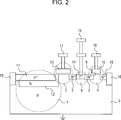
2 ist eine Schnittansicht, die die Struktur eines Bildpunkts der Festkörperbildaufnahmevorrichtung gemäß dem ersten Ausführungsbeispiel der vorliegenden Erfindung darstellt. 2 FIG. 10 is a sectional view illustrating the structure of a pixel of the solid state image pickup device according to the first embodiment of the present invention. FIG.
3 ist ein äquivalentes Schaltungsdiagram, das Bildpunkte einer Festkörperbildaufnahmevorrichtung gemäß einem zweiten Ausführungsbeispiel der vorliegenden Erfindung darstellt. 3 Fig. 12 is an equivalent circuit diagram illustrating pixels of a solid state imaging device according to a second embodiment of the present invention.
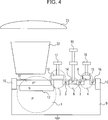
4 ist eine Schnittansicht, die die Struktur eines Bildpunkts einer Festkörperbildaufnahmevorrichtung gemäß einem dritten Ausführungsbeispiel der vorliegenden Erfindung darstellt. 4 FIG. 10 is a sectional view illustrating the structure of a pixel of a solid-state image sensing device according to a third embodiment of the present invention. FIG.
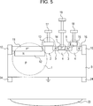
5 ist eine Schnittansicht, die die Struktur eines Bildpunkts einer Festkörperbildaufnahmevorrichtung gemäß einem vierten Ausführungsbeispiel der vorliegenden Erfindung darstellt. 5 FIG. 10 is a sectional view illustrating the structure of a pixel of a solid state image pickup device according to a fourth embodiment of the present invention. FIG.
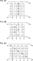
6A ist eine schematische Ansicht, die eine Anordnung von Bildpunkten einer Festkörperbildaufnahmevorrichtung gemäß der vorliegenden Erfindung darstellt. 6A Fig. 12 is a schematic view illustrating an arrangement of pixels of a solid state image pickup device according to the present invention.
6B ist eine schematische Ansicht, die eine andere Anordnung von Bildpunkten einer Festkörperbildaufnahmevorrichtung gemäß der vorliegenden Erfindung darstellt. 6B Fig. 10 is a schematic view illustrating another arrangement of pixels of a solid-state image pickup device according to the present invention.
6C ist eine schematische Ansicht, die eine andere Anordnung von Bildpunkten einer Festkörperbildaufnahmevorrichtung gemäß der vorliegenden Erfindung darstellt. 6C Fig. 10 is a schematic view illustrating another arrangement of pixels of a solid-state image pickup device according to the present invention.
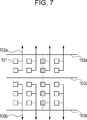
7 ist eine schematische Ansicht, die eine andere Anordnung von Bildpunkten einer Festkörperbildaufnahmevorrichtung gemäß der vorliegenden Erfindung darstellt. 7 Fig. 10 is a schematic view illustrating another arrangement of pixels of a solid-state image pickup device according to the present invention.
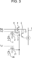
8 ist ein Ablaufdiagram, das Impulse zum Ansteuern der Festkörperbildaufnahmevorrichtung gemäß dem ersten Ausführungsbeispiel der vorliegenden Erfindung darstellt. 8th FIG. 10 is a flow chart illustrating pulses for driving the solid-state image pickup device according to the first embodiment of the present invention. FIG.
Beschreibung von AusführungsbeispielenDescription of exemplary embodiments
Ausführungsbeispiele der vorliegenden Erfindung werden nachstehend mit Bezug auf die Zeichnungen detailliert beschrieben. 1 ist ein äquivalentes Schaltungsdiagram, das eine Festkörperbildaufnahmevorrichtung gemäß einem ersten Ausführungsbeispiel der vorliegenden Erfindung darstellt. In 1 sind die Elemente, die von der gestrichelten Linie umgeben sind, in einem Bildpunkt 10a enthalten. Das äquivalente Schaltungsdiagram in 1 zeigt eine Konfiguration, in welcher sechs Bildpunkte in drei Zeilen und zwei Spalten angeordnet sind. Die Elemente mit ähnlichen Funktionen in jedem Bildpunkt 10 sind durch dieselben Bezugszeichen gekennzeichnet, und werden durch Hinzufügen unterschiedlicher alphabetischer Buchstaben zu den entsprechenden Zahlen für die Elemente der einzelnen Bildpunkte 10 unterschieden. Die vorliegende Erfindung ist auf die vorstehend beschriebene Anzahl an Bildpunkten nicht beschränkt, und es reicht aus, dass eine Vielzahl von Bildpunkten in einer Matrix angeordnet ist.Embodiments of the present invention will be described below in detail with reference to the drawings. 1 Fig. 12 is an equivalent circuit diagram illustrating a solid-state imaging device according to a first embodiment of the present invention. In 1 are the elements that are surrounded by the dashed line, in one pixel 10a contain. The equivalent circuit diagram in 1 shows a configuration in which six Pixels are arranged in three rows and two columns. The elements with similar functions in each pixel 10 are denoted by the same reference numerals, and become the corresponding numbers for the elements of the individual pixels by adding different alphabetic letters 10 distinguished. The present invention is not limited to the above-described number of pixels, and it is sufficient that a plurality of pixels are arranged in a matrix.
Die in 1 gezeigten Elemente, die jeden Bildpunkt 10 der Festkörperbildaufnahmevorrichtung ausbilden, werden nachstehend beschrieben. Eine fotoelektrische Umwandlungseinheit 1, wie beispielsweise eine Fotodiode, erzeugt eine elektrische Ladung. Ein Transfer-MOS-Transistor 2 überträgt eine in der fotoelektrischen Umwandlungseinheit 1 erzeugte elektrische Ladung. Eine Steuerelektrode 3 eines Verstärkungstransistors 6 empfängt eine in der fotoelektrischen Umwandlungseinheit 1 erzeugte elektrische Ladung. Ein Reset-MOS-Transistor 4 wird zum Anlegen einer Reset-Spannung an die Steuerelektrode 3 verwendet. Der Transfer-MOS-Transistor 2 und der Reset-MOS-Transistor 4 sind vom N-Leitfähigkeitstyp. Der Verstärkungstransistor 6, wie beispielsweise ein P-Typ-Sperrschichtfeldeffekttransistor (nachstehend JFET genannt; JFET: ”junction field effect transistor”), verstärkt eine in der fotoelektrischen Umwandlungseinheit 1 erzeugte Signalladung. Ein Koppelkondensator 8 ist zwischen dem Gate des Reset-MOS-Transistors 4 und der Steuerelektrode 3 angeordnet. Eine Ausgabesignalleitung 7 ist mit einer Konstantstromquelle I verbunden und bildet zusammen mit dem Verstärkungstransistor 6, welcher ein P-Typ-JFET ist, einen Sourcefolger.In the 1 shown elements representing each pixel 10 of the solid state image pickup device will be described below. A photoelectric conversion unit 1 , such as a photodiode, generates an electrical charge. A transfer MOS transistor 2 transmits one in the photoelectric conversion unit 1 generated electric charge. A control electrode 3 an amplification transistor 6 receives one in the photoelectric conversion unit 1 generated electric charge. A reset MOS transistor 4 is used to apply a reset voltage to the control electrode 3 used. The transfer MOS transistor 2 and the reset MOS transistor 4 are of the N-conductivity type. The amplification transistor 6 such as a P-type junction field-effect transistor (hereinafter called JFET: junction field effect transistor) amplifies one in the photoelectric conversion unit 1 generated signal charge. A coupling capacitor 8th is between the gate of the reset MOS transistor 4 and the control electrode 3 arranged. An output signal line 7 is connected to a constant current source I and forms together with the amplification transistor 6 , which is a P-type JFET, a source follower.
Ein Reset-Impuls Res wird in das Gate des Reset-MOS-Transistors 4 eingegeben, während ein Übertragungsimpuls Tx in das Gate des Transfer-MOS-Transistors 2 eingegeben wird. Der Reset-MOS-Transistor 4 und der Transfer-MOS-Transistor 2 können jeweils durch den Reset-Impuls Res und den Transfer-Impuls Tx gesteuert werden, um entweder in dem leitenden Zustand oder in dem nichtleitenden Zustand zu sein. Reset-Energieversorgungsleitungen VRES1 und VRES2 werden für die Bildpunkte 10, die an den Enden einer Matrix in der Spaltenrichtung angeordnet sind, bereitgestellt, um eine Reset-Spannung zum Rücksetzen der Steuerelektroden 3 anzulegen. Die Reset-Energieversorgungsleitungen VRES1 und VRES2 können auch zum Rücksetzen der fotoelektrischen Umwandlungseinheit 1 verwendet werden.A reset pulse Res is placed in the gate of the reset MOS transistor 4 while a transfer pulse Tx enters the gate of the transfer MOS transistor 2 is entered. The reset MOS transistor 4 and the transfer MOS transistor 2 can each be controlled by the reset pulse Res and the transfer pulse Tx to be either in the conducting state or in the non-conducting state. Reset power supply lines VRES1 and VRES2 are used for the pixels 10 provided at the ends of a matrix in the column direction, provided with a reset voltage for resetting the control electrodes 3 to apply. The reset power supply lines VRES1 and VRES2 may also be used to reset the photoelectric conversion unit 1 be used.
Eine Signalausgabe von dem Verstärkungstransistor 6 von jedem Bildpunkt 10 wird an die Ausgabesignalleitung 7 ausgelesen. Um eine schnelle Signalverarbeitung zu erzielen, werden in diesem Ausführungsbeispiel Signale von den Bildpunkten 10a und 10b, welche in der Zeilenrichtung angeordnet sind, jeweils an die Ausgabesignalleitungen 7x und 7y parallel ausgelesen. In ähnlicher Weise werden Signale von den Bildpunkten 10c und 10d jeweils an die Ausgabesignalleitungen 7x und 7y parallel ausgelesen, und dann werden Signale von den Bildpunkten 10e und 10f jeweils an die Ausgabesignalleitungen 7x und 7y parallel ausgelesen. Signale von den Bildpunkten 10a, 10c und 10e, welche in der Spaltenrichtung angeordnet sind, werden nicht parallel ausgelesen.A signal output from the amplification transistor 6 from every pixel 10 is applied to the output signal line 7 read. In order to achieve a fast signal processing, in this embodiment, signals from the pixels 10a and 10b which are arranged in the row direction, respectively to the output signal lines 7x and 7y read in parallel. Similarly, signals from the pixels 10c and 10d each to the output signal lines 7x and 7y read in parallel, and then signals from the pixels 10e and 10f each to the output signal lines 7x and 7y read in parallel. Signals from the pixels 10a . 10c and 10e which are arranged in the column direction are not read in parallel.
In diesem Ausführungsbeispiel ist der Reset-MOS-Transistor 4a jeweils in einem elektrischen Pfad zwischen den Steuerelektroden 3a und 3c der Verstärkungstransistoren 6a und 6c der beiden Bildpunkte 10a und 10c angeordnet, welche in der Spaltenrichtung angeordnet sind. Der Reset-MOS-Transistor 4a steuert eine elektrische Verbindung zwischen der Steuerelektrode 3a des Verstärkungstransistors 6a und der Steuerelektrode 3c des Verstärkungstransistors 6c. Ein Reset-MOS-Transistor 4x ist in einem elektrischen Pfad zwischen der Steuerelektrode 3a des Verstärkungstransistors 6a und der Reset-Energieversorgungsleitung VRES1 angeordnet. Der Reset-MOS-Transistor 4x steuert eine elektrische Verbindung zwischen dem Steueranschluss 3a des Verstärkungstransistor 6a und der Reset-Energieversorgungsleitung VRES1. Ein Reset-MOS-Transistor 4c ist in einem elektrischen Pfad zwischen der Steuerelektrode 3c des Verstärkungstransistors 6c und der Reset-Energieversorgungsleitung VRES2 angeordnet. Der Reset-MOS-Transistor 4c steuert eine elektrische Verbindung zwischen der Steuerelektrode 3c des Verstärkungstransistors 6c und der Reset-Energieversorgungsleitung VRES2. In ähnlicher Weise ist ein Reset-MOS-Transistor zwischen den Steuerelektroden der in benachbarten Bildpunkten enthaltenden Verstärkungstransistoren oder zwischen der Steuerelektrode und der entsprechenden Reset-Energieversorgungsleitung angeordnet, um die Steuerelektroden der benachbarten Bildpunkte oder die Steuerelektrode und die Reset-Energieversorgungsleitung elektrisch zu verbinden.In this embodiment, the reset MOS transistor 4a each in an electrical path between the control electrodes 3a and 3c the amplification transistors 6a and 6c of the two pixels 10a and 10c arranged, which are arranged in the column direction. The reset MOS transistor 4a controls an electrical connection between the control electrode 3a the amplification transistor 6a and the control electrode 3c the amplification transistor 6c , A reset MOS transistor 4x is in an electrical path between the control electrode 3a the amplification transistor 6a and the reset power supply line VRES1. The reset MOS transistor 4x controls an electrical connection between the control terminal 3a the amplification transistor 6a and the reset power supply line VRES1. A reset MOS transistor 4c is in an electrical path between the control electrode 3c the amplification transistor 6c and the reset power supply line VRES2. The reset MOS transistor 4c controls an electrical connection between the control electrode 3c the amplification transistor 6c and the reset power supply line VRES2. Similarly, a reset MOS transistor is disposed between the control electrodes of the amplifying transistors included in adjacent pixels or between the control electrode and the corresponding reset power supply line to electrically connect the control electrodes of the adjacent pixels or the control electrode and the reset power supply line.
Auf diese Weise werden die Steuerelektroden 3 der in einer Vielzahl von Bildpunkten enthaltenen Verstärkungstransistoren 6, aus welchen Signale nicht parallel ausgelesen werden, durch die Reset-MOS-Transistoren 4 in der Spaltenrichtung in Reihe geschaltet. Unter der Vielzahl von in Reihe geschalteten Steuerelektroden 3 werden die an den Enden in der Spaltenrichtung angeordneten Steuerelektroden 3 mit den Reset-Energieversorgungsleitungen VRES1 und VRES2 durch die unterschiedlichen Reset-MOS-Transistoren 4 verbunden. Deshalb kann in diesem Ausführungsbeispiel die Steuerelektrode 3 von jedem Bildpunkt sowohl mit der ersten Reset-Energieversorgungseinheit (Reset-Energieversorgungsleitung VRES1) als auch der zweiten Reset-Energieversorgungseinheit (Reset-Energieversorgungsleitung VRES2) über einen oder mehrere Reset-MOS-Transistoren 4 elektrisch verbunden werden. Die Anzahl an Reset-MOS-Transistoren 4 ist um eins größer als die Anzahl an in jeder Spalte enthaltenen Bildpunkten.In this way, the control electrodes 3 the amplification transistors included in a plurality of pixels 6 from which signals are not read in parallel, by the reset MOS transistors 4 connected in series in the column direction. Among the plurality of control electrodes connected in series 3 become the control electrodes arranged at the ends in the column direction 3 with the reset power supply lines VRES1 and VRES2 through the different reset MOS transistors 4 connected. Therefore, in this embodiment, the control electrode 3 from each pixel both with the first reset power supply unit (reset Power supply line VRES1) and the second reset power supply unit (reset power supply line VRES2) via one or more reset MOS transistors 4 be electrically connected. The number of reset MOS transistors 4 is one greater than the number of pixels in each column.
In dem elektrischen Pfad zwischen der Steuerelektrode 3c und der Reset-Energieversorgungsleitung VRES2 wird die Steuerelektrode 3a und der Reset-MOS-Transistor 4e zusätzlich zu dem Reset-MOS-Transistor 4c, wie in 1 gezeigt, angeordnet. Auf diese Weise können in dem elektrischen Pfad, für welchen der Reset-MOS-Transistor 4c eine elektrische Verbindung steuert, andere Elemente angeordnet werden. Beispielsweise können in einer Festkörperbildaufnahmevorrichtung, in welcher zehn Millionen oder mehr Bildpunkte in einer Matrix angeordnet sind, zwischen der Steuerelektrode eines bestimmten Bildpunkts und einer Reset-Energieversorgungseinheit die Steuerelektroden von Verstärkungstransistoren und Reset-Transistoren, die in mehreren tausend Bildpunkten enthalten sind, angeordnet werden.In the electrical path between the control electrode 3c and the reset power supply line VRES2 becomes the control electrode 3a and the reset MOS transistor 4e in addition to the reset MOS transistor 4c , as in 1 shown, arranged. In this way, in the electrical path for which the reset MOS transistor 4c controls an electrical connection, other elements are arranged. For example, in a solid state image pickup device in which ten million or more pixels are arranged in a matrix, between the control electrode of a certain pixel and a reset power supply unit, the control electrodes of amplifying transistors and reset transistors included in several thousands of pixels may be arranged.
Mit der Konfiguration, die die in 1 gezeigten Steuerelektroden 3 und die Reset-MOS-Transistoren 4 aufweist, wenn ein Rücksetzen durchgeführt wird, genügt es, dass lediglich eine Steuerelektrode in jeder Spalte rückgesetzt wird. Somit sind eine parasitäre Kapazität und ein Streuwiderstand klein. Dies wird nachstehend detailliert diskutiert.With the configuration that the in 1 shown control electrodes 3 and the reset MOS transistors 4 When a reset is performed, it is sufficient that only one control electrode in each column is reset. Thus, a parasitic capacitance and a stray resistance are small. This will be discussed in detail below.
2 ist ein Schnittdiagram, das ein Bildpunktgebiet in der Festkörperbildaufnahmevorrichtung gemäß diesem Ausführungsbeispiel darstellt. Die Elemente, die den in 1 gezeigten entsprechen, sind durch dieselben Bezugszeichen gekennzeichnet. Der Bildpunktbereich ist ein Bereich, in welchem Bildpunkte in einer Matrix auf einem Halbleitersubstrat angeordnet sind. Der Bildpunktbereich kann ein Teil des Halbleitersubstrats oder die Gesamtheit des Halbleitersubstrats sein. 2 FIG. 10 is a sectional diagram illustrating a pixel area in the solid-state imaging device according to this embodiment. FIG. The elements that make up the in 1 shown are indicated by the same reference numerals. The pixel area is a region in which pixels are arranged in a matrix on a semiconductor substrate. The pixel region may be a part of the semiconductor substrate or the entirety of the semiconductor substrate.
In 2 wird ein P-Typ-Halbleiterbereich 9, aus einem Isolator ausgebildete Vorrichtungsisolationsabschnitte 10, ein P-Typ-Halbleiterbereich 11, der auf der lichteinfallenden Oberfläche angeordnet ist, und ein N-Typ-Halbleiterbereich 12, der darin eine Signalladung speichert, gezeigt. Jeder der P-Typ-Halbleiterbereiche 9 und 11 bildet eine PN-Sperrschicht mit dem N-Typ-Halbleiterbereich 12 aus, und die P-Typ-Halbleiterbereiche 9 und 11 und der N-Typ-Halbleiterbereich 12 bilden die fotoelektrische Umwandlungseinheit 1 aus. In 2 wird auch eine Gate-Elektrode 13 des Transfer-MOS-Transistors 2 gezeigt.In 2 becomes a P-type semiconductor region 9 , device isolation sections formed of an insulator 10 , a P-type semiconductor region 11 which is disposed on the light-incident surface, and an N-type semiconductor region 12 showing a signal charge stored therein. Each of the P-type semiconductor regions 9 and 11 forms a PN junction with the N-type semiconductor region 12 out, and the P-type semiconductor regions 9 and 11 and the N-type semiconductor region 12 form the photoelectric conversion unit 1 out. In 2 will also be a gate electrode 13 of the transfer MOS transistor 2 shown.
Die in 1 gezeigte Steuerelektrode 3 ist aus einem N-Typ-Halbleiterbereich ausgebildet, und der N-Typ-Halbleiterbereich, der der Steuerelektrode 3 entspricht, ist durch dasselbe Bezugszeichen in 2 gekennzeichnet. Nachstehend wird in dieser Beschreibung, wenn die Steuerelektrode einen Schaltungsknoten darstellt, er als die Steuerelektrode bezeichnet, und wenn die Steuerelektrode einen Halbleiterbereich eines Bildpunkts in einem Querschnitt darstellt, er als der Steuerelektrodenbereich bezeichnet. Ein P-Typ-Halbleiterbereich 14 ist von dem Steuerelektrodenbereich 3 in der Ebene auf derselben Höhe wie die Substratoberfläche umgeben. Der Verstärkungstransistor 6, welcher ein P-Typ-JFET ist, ist aus dem P-Typ-Halbleiterbereich 14 ausgebildet, welcher ein Source-Bereich ist, dem Steuerelektrodenbereich 3 und dem P-Typ-Halbleiterbereich 9, welcher ein Drain-Bereich ist. Der P-Typ-Halbleiterbereich 9 kann das Halbleitersubstrat selbst oder ein in dem Halbleitersubstrat ausgebildeter Quellenbereich sein.In the 1 shown control electrode 3 is formed of an N-type semiconductor region, and the N-type semiconductor region, that of the control electrode 3 is the same reference numeral in FIG 2 characterized. Hereinafter, in this specification, when the control electrode represents a circuit node, it is referred to as the control electrode, and when the control electrode represents a semiconductor region of a pixel in a cross section, it is referred to as the control electrode region. A P-type semiconductor region 14 is from the control electrode area 3 surrounded in the plane at the same height as the substrate surface. The amplification transistor 6 which is a P-type JFET is of the P-type semiconductor region 14 formed, which is a source region, the control electrode region 3 and the P-type semiconductor region 9 , which is a drain region. The P-type semiconductor region 9 may be the semiconductor substrate itself or a source region formed in the semiconductor substrate.
In 2 wird auch eine Gate-Elektrode 15 des Reset-MOS-Transistors 4 und ein Steuerelektrodenbereich 16 eines benachbarten Bildpunkts in der Spaltenrichtung gezeigt. In diesem Ausführungsbeispiel dient in dem Reset-MOS-Transistor 4, der die Steuerelektroden 3 von benachbarten Bildpunkten verbindet, der Steuerelektrodenbereich 3 eines Bildpunkts als der Sourcebereich des MOS-Transistors 4, und der Steuerelektrodenbereich 16 des anderen Bildpunkts dient als der Drain-Bereich des MOS-Transistors 4.In 2 will also be a gate electrode 15 of the reset MOS transistor 4 and a control electrode area 16 of an adjacent pixel in the column direction. In this embodiment, in the reset MOS transistor is used 4 , the control electrodes 3 from adjacent pixels, the control electrode area 3 of a pixel as the source region of the MOS transistor 4 , and the control electrode area 16 the other pixel serves as the drain region of the MOS transistor 4 ,
Der Koppelkondensator 8 wird in dem überlappenden Abschnitt zwischen der Gate-Elektrode 15 des Reset-MOS-Transistors 4 und dem Steuerelektrodenbereich 3 erzeugt, und enthält den Gate-Oxidfilm des Reset-MOS-Transistors 4. Eine Steuerleitung 17 zum Übertragen eines Transfer-Impulses Tx ist mit der Gate-Elektrode 13 verbunden. Eine Steuerleitung 18 zum Übertragen eines Reset-Impulses Res ist mit der Gate-Elektrode 15 verbunden. Eine Signalleitung 19 ist mit dem P-Typ-Halbleiterbereich 14 verbunden, welcher den Source-Bereich des Verstärkungstransistors 6 darstellt. Die Signalleitung 19 bildet eine Ausgabesignalleitung aus, an welche Signale von den Verstärkungstransistoren 6 ausgelesen werden. Die Steuerleitungen 17 und 18 sind in der Zeilenrichtung angeordnet.The coupling capacitor 8th is in the overlapping portion between the gate electrode 15 of the reset MOS transistor 4 and the control electrode area 3 and contains the gate oxide film of the reset MOS transistor 4 , A control line 17 for transmitting a transfer pulse Tx is with the gate electrode 13 connected. A control line 18 for transmitting a reset pulse Res is connected to the gate electrode 15 connected. A signal line 19 is with the P-type semiconductor region 14 connected to the source region of the amplification transistor 6 represents. The signal line 19 forms an output signal line to which signals from the amplification transistors 6 be read out. The control lines 17 and 18 are arranged in the row direction.
In diesem Ausführungsbeispiel sind, wie in 1 gezeigt, die Reset-Energieversorgungsleitungen VRES1 und VRES2 für die Bildpunkte bereitgestellt, die an den Enden einer Matrix in der Spaltenrichtung angeordnet sind. Mit der Konfiguration, in welcher Reset-Energieversorgungseinheiten wie in diesem Ausführungsbeispiel außerhalb des Bildpunktbereichs angeordnet sind, ist es nicht erforderlich, eine Verdrahtung zum Bereitstellen einer Reset-Energieversorgung für den Bildpunktbereich anzuordnen.In this embodiment, as in FIG 1 shown, the reset power supply lines VRES1 and VRES2 provided for the pixels, which are arranged at the ends of a matrix in the column direction. With the configuration in which reset power supply units are arranged outside the pixel area as in this embodiment, it is not necessary to arrange a wiring for providing a reset power supply to the pixel area.
Nachstehend wird der Betrieb der Festkörperbildaufnahmevorrichtung gemäß diesem Ausführungsbeispiel beschrieben. In diesem Ausführungsbeispiel wird angenommen, dass in dem Initialisierungszustand alle Bildpunkte 10 rückgesetzt sind. D. h., in diesem Zustand befinden sich alle Reset-MOS-Transistoren 4 in dem leitenden Zustand, und eine Reset-Spannung ist an die Steuerelektroden 3 aller Bildpunkte 10 angelegt. Dann wird eine Zeile ausgewählt, von welcher Signale ausgelesen werden, und Signale, die von den Bildpunkten 10 ausgelesen werden, die in der ausgewählten Zeile enthalten sind, werden an die entsprechende Ausgabesignalleitung 7 ausgelesen. Next, the operation of the solid-state image pickup device according to this embodiment will be described. In this embodiment, it is assumed that all the pixels in the initialization state 10 are reset. That is, in this state, all reset MOS transistors are located 4 in the conducting state, and a reset voltage is applied to the control electrodes 3 all pixels 10 created. Then a line is selected from which signals are read out and signals from the pixels 10 which are included in the selected row are applied to the corresponding output signal line 7 read.
Der spezifische Betrieb wird nachstehend mit Bezug auf 8 beschrieben. 8 zeigt Reset-Impulse Res0, Res1, Res2 und Res3, die in die Gates der Reset-MOS-Transistoren 4 eingegeben werden, und Transfer-Impulse Tx1, Tx2 und Tx3, die in die Gates der Transfer-MOS-Transistoren 2 eingegeben werden. Jeder Impuls wird in das Gate des entsprechenden in 1 gezeigten Transistors eingegeben. Eine Spannung zum Bewirken, dass sich der Reset-MOS-Transistor 4 und der Transfer-MOS-Transistor 2 in dem leitenden Zustand befinden, wird als der Hochpegel bezeichnet, und eine Spannung zum Bewirken, dass sich der Reset-MOS-Transistor 4 und der Transfer-MOS-Transistor 2 in dem nichtleitenden Zustand befinden, wird als der Niedrigpegel bezeichnet. Der Hochpegel wird eingestellt, um beispielsweise das Energieversorgungspotential VDD darzustellen. Der Niedrigpegel wird eingestellt, um beispielsweise das GND-Potential oder das negative Potential darzustellen. In 8 werden Potentialänderungen V1, V2, und V3 jeweils der Steuerelektroden 3a, 3c, und 3e schematisch gezeigt.The specific operation will be described below with reference to FIG 8th described. 8th shows reset pulses Res0, Res1, Res2 and Res3, which are in the gates of the reset MOS transistors 4 are input, and transfer pulses Tx1, Tx2 and Tx3, which are in the gates of the transfer MOS transistors 2 be entered. Each impulse is in the gate of the corresponding in 1 shown transistor entered. A voltage to cause the reset MOS transistor 4 and the transfer MOS transistor 2 are in the conductive state is referred to as the high level, and a voltage for causing the reset MOS transistor 4 and the transfer MOS transistor 2 in the non-conductive state is referred to as the low level. The high level is set to represent, for example, the power supply potential VDD. The low level is set to represent, for example, the GND potential or the negative potential. In 8th Potential changes V1, V2, and V3 are respectively the control electrodes 3a . 3c , and 3e shown schematically.
Der Betrieb zum Auswählen einer Zeile von Bildpunkten 10, aus welchen Signale ausgegeben werden, wird zunächst nachstehend beschrieben. Es ist erforderlich, dass sich das Potential der Steuerelektroden 3 der Verstärkungstransistoren 6, die in den Bildpunkten 10 in der ausgewählten Zeile enthalten sind, in dem schwebenden (erdfreien) Zustand befinden. Da die Verstärkungstransistoren 6 von dem P-Typ sind, ist es in diesem Ausführungsbeispiel auch erforderlich, dass unter den Steuerelektroden 3 der Verstärkungstransistoren 6 der Vielzahl von Bildpunkten 10, die mit der gemeinsamen Ausgabesignalleitung 7 verbunden sind, das Potential der Steuerelektrode 3 des Verstärkungstransistor 6 des Bildpunkts 10 in der ausgewählten Zeile das niedrigste ist. In diesem Zustand fließt der von der Ausgabesignalleitung 7 zugeführte konstante Strom lediglich in den Verstärkungstransistor 6 des ausgewählten Bildpunkts 10, und das dem Potential der Steuerelektrode 3 des Verstärkungstransistors 6 des ausgewählten Bildpunkts 10 entsprechende Potential wird an die Ausgabesignalleitung 7 durch den Sourcefolgerbetrieb des Verstärkungstransistors 6 und der Ausgabesignalleitung 7 ausgegeben. Falls der Verstärkungstransistor 6 von dem N-Typ ist, ist es erforderlich, dass unter den Steuerelektroden 3 der Verstärkungstransistoren 6 der Vielzahl von Bildpunkten 10, die mit der gemeinsamen Ausgabesignalleitung 7 verbunden sind, das Potential der Steuerelektrode 3 des Verstärkungstransistors 6 des Bildpunkts 10 in der ausgewählten Zeile das höchste ist.The operation of selecting a row of pixels 10 from which signals are output will first be described below. It is necessary that the potential of the control electrodes 3 the amplification transistors 6 that in the pixels 10 contained in the selected line are in the floating (floating) state. Since the amplification transistors 6 of the P-type, it is also required in this embodiment that under the control electrodes 3 the amplification transistors 6 the multitude of pixels 10 connected to the common output signal line 7 connected, the potential of the control electrode 3 the amplification transistor 6 of the pixel 10 in the selected line is the lowest. In this state, the current flows from the output signal line 7 supplied constant current only in the amplifying transistor 6 of the selected pixel 10 , and that the potential of the control electrode 3 the amplification transistor 6 of the selected pixel 10 corresponding potential is applied to the output signal line 7 by the source follower operation of the amplification transistor 6 and the output signal line 7 output. If the amplification transistor 6 of the N type, it is necessary that under the control electrodes 3 the amplification transistors 6 the multitude of pixels 10 connected to the common output signal line 7 connected, the potential of the control electrode 3 the amplification transistor 6 of the pixel 10 in the selected line is the highest.
In diesem Ausführungsbeispiel ist das Reset-Potential VRES das Potential zwischen dem GND-Potential und dem Energieversorgungspotential VDD. Bevor eine Zeile ausgewählt wird, befinden sich alle Reset-Impulse auf dem Hochpegel und alle Reset-MOS-Transistoren 4 befinden sich in dem leitenden Zustand. Demgemäß werden die Potentiale der Steuerelektroden 3 aller Bildpunkte 10 eingestellt, um auf dem Reset-Potential VRES zu sein.In this embodiment, the reset potential VRES is the potential between the GND potential and the power supply potential VDD. Before a row is selected, all reset pulses are high and all reset MOS transistors 4 are in the conductive state. Accordingly, the potentials of the control electrodes become 3 all pixels 10 set to be at the reset potential VRES.
Wenn eine bestimmte Zeile von Bildpunkten 10 ausgewählt ist, werden die Reset-Impulse, die in das Paar von Reset-MOS-Transistoren 4 eingegeben sind, die die Steuerelektrode 3 des Bildpunkts 10 in der ausgewählten Zeile umgeben, eingestellt, um auf dem Niedrigpegel zu sein. Wenn beispielsweise die Bildpunkte 10c und 10d in der zweiten Zeile ausgewählt sind, werden die Reset-Impulse RES1 und RES2 von dem Hochpegel auf den Niedrigpegel geändert, und die Reset-Impulse Res0 und Res3 werden, wie durch den Zeitpunkt T1 in 8 angezeigt, auf dem Hochpegel gehalten. Es wird bewirkt, dass die Reset-MOS-Transistoren 4a und 4b, in welche der Reset-Impuls Res1 eingegeben ist, in dem nichtleitenden Zustand eingestellt sind, und dass die Reset-MOS-Transistoren 4c und 4d, in welche der Reset-Impuls Res2 eingegeben ist, auch in dem nichtleitenden Zustand eingestellt sind. Demgemäß wird bewirkt, dass sich die Potentiale der Steuerelektroden 3 der Bildpunkte 10 in der zweiten Zeile in dem schwebenden (erdfreien) Zustand befinden.If a particular line of pixels 10 is selected, the reset pulses that are in the pair of reset MOS transistors 4 are entered, which are the control electrode 3 of the pixel 10 Surrounded in the selected line, set to be at the low level. For example, if the pixels 10c and 10d are selected in the second row, the reset pulses RES1 and RES2 are changed from the high level to the low level, and the reset pulses Res0 and Res3 become as indicated by the time T1 in FIG 8th displayed, kept at the high level. It causes the reset MOS transistors 4a and 4b in which the reset pulse Res1 is input are set in the non-conductive state, and that the reset MOS transistors 4c and 4d into which the reset pulse Res2 is input are also set in the non-conductive state. Accordingly, causes the potentials of the control electrodes 3 of the pixels 10 in the second row in the floating (floating) state.
In diesem Ausführungsbeispiel sind die Reset-MOS-Transistoren 4 von dem N-Typ, und das Potential des Niedrigpegels ist niedriger als das Potential des Hochpegels. Wenn die Reset-Impulse Res1 und Res2 auf den Niedrigpegel geändert werden, wird das Potential der Steuerelektroden 3 der in der zweiten Zeile enthaltenen Bildpunkte 10 über die Koppelkondensatoren 8 verringert (V2 in 8). Die Potentiale der Steuerelektroden 3 der in der ersten Zeile und der neben der zweiten Zeile liegenden dritten Zeile enthaltenen Bildpunkte 10 werden auch augenblicklich verringert, indem sie durch die Potentialänderung aufgrund der Reset-Impulse Res1 und Res2 beeinflusst werden (V1 und V3 in 8). Da jedoch die Reset-Impulse Res0 und Res3 auf dem Hochpegel gehalten werden, kehren die Potentiale der Steuerelektroden 3 der neben dem ausgewählten Bildpunkt 10 liegenden Bildpunkte 10 auf das Reset-Potential VRES zurück. Unter den Potentialen der mit der gemeinsamen Ausgabesignalleitung 7 verbundenen Bildpunkte 10 wird das Potential der Steuerelektrode 3 des Verstärkungstransistors 6 des in der zweiten Zeile enthaltenen Bildpunkts 10 das niedrigste. Indem der vorstehend beschriebene Betrieb durchgeführt wird, wird die zweite Zeile ausgewählt.In this embodiment, the reset MOS transistors 4 of the N-type, and the potential of the low level is lower than the potential of the high level. When the reset pulses Res1 and Res2 are changed to the low level, the potential of the control electrodes becomes 3 the pixels contained in the second line 10 over the coupling capacitors 8th reduced (V2 in 8th ). The potentials of the control electrodes 3 the pixels contained in the first line and the third line adjacent to the second line 10 are also momentarily reduced by being affected by the potential change due to the reset pulses Res1 and Res2 (V1 and V3 in FIG 8th ). However, since the reset pulses Res0 and Res3 are maintained at the high level, the potentials of the control electrodes are reversed 3 the next to the selected pixel 10 lying pixels 10 on the reset Potential VRES back. Among the potentials of the common output signal line 7 connected pixels 10 becomes the potential of the control electrode 3 the amplification transistor 6 of the pixel contained in the second line 10 the lowest. By performing the above-described operation, the second line is selected.
In diesem Ausführungsbeispiel wird bewirkt, dass sich die beiden Reset-MOS-Transistoren 4, die direkt mit der Steuerelektrode 3 des ausgewählten Bildpunkts verbunden sind, in dem nichtleitenden Zustand befinden, und dass sich die anderen Reset-MOS-Transistoren 4 in dem leitenden Zustand befinden, wodurch das Potential der Steuerelektrode 3 des ausgewählten Bildpunkts 10 über den Koppelkondensator 8 gesteuert werden kann.In this embodiment, causes the two reset MOS transistors 4 which is directly connected to the control electrode 3 of the selected pixel are in the non-conductive state, and that the other reset MOS transistors 4 in the conductive state, whereby the potential of the control electrode 3 of the selected pixel 10 over the coupling capacitor 8th can be controlled.
Nach dem Auswählen der Bildpunkte 10 in der zweiten Zeile wird zum Zeitpunkt T2 in 8 ein Hochpegelimpuls dem Transferimpuls Tx2 zugeführt, und eine elektrische Ladung in der fotoelektrischen Umwandlungseinheit 1 wird an die Steuerelektrode 3 übertragen. Die Größe, um welche sich das Potential der Steuerelektrode 3 verringert, wird durch die Größe der in der fotoelektrischen Umwandlungseinheit 1 erzeugten elektrischen Ladung bestimmt. Die den Transfer-MOS-Transistoren 2 zugeführten Transferimpulse lauten von unten in 1 gesehen Tx1, Tx2, und Tx3. Nach der Übertragung einer elektrischen Ladung an die Steuerelektrode 3 wird die Ausgabe gemäß dem Potential der Steuerelektrode 3 an die Ausgabesignalleitung 7 ausgelesen.After selecting the pixels 10 in the second line, at time T2 in 8th a high-level pulse is supplied to the transfer pulse Tx2, and an electric charge in the photoelectric conversion unit 1 goes to the control electrode 3 transfer. The size by which the potential of the control electrode 3 is reduced by the size of the in the photoelectric conversion unit 1 determined electrical charge generated. The transfer MOS transistors 2 supplied transfer pulses are from below in 1 seen Tx1, Tx2, and Tx3. After transferring an electrical charge to the control electrode 3 the output becomes according to the potential of the control electrode 3 to the output signal line 7 read.
Nachstehend wird der Rücksetzbetrieb für jeden Bildpunkt beschrieben. Das Potential der Reset-Energieversorgungsleitungen ist das Potential VRES zwischen dem Hochpegel und dem Niedrigpegel.Hereinafter, the reset operation for each pixel will be described. The potential of the reset power supply lines is the potential VRES between the high level and the low level.
Wie vorstehend beschrieben wird der Hochpegelimpuls an die Gates der Reset-MOS-Transistoren 4 angelegt, mit Ausnahme von den neben dem ausgewählten Bildpunkt 10 angeordneten Reset-MOS-Transistoren 4. Insbesondere sind die Reset-Impulse Res0 und Res3 während der Periode zwischen T1 und T3 in 8 auf dem Hochpegel, während die Reset-Impulse Res1 und Res2, die den Reset-MOS-Transistoren 4 neben dem ausgewählten Bildpunkt 10 angelegt werden, auf dem Niedrigpegel sind. Demgemäß befinden sich die Reset-MOS-Transistoren 4x, 4y, 4e und 4f in 1 in dem leitenden Zustand, während die Potentiale der Steuerelektroden 3 (V1 und V3) der Bildpunkte 10, welche nicht ausgewählt sind, auf dem Reset-Potential VRES gehalten werden.As described above, the high level pulse is applied to the gates of the reset MOS transistors 4 created, except for those next to the selected pixel 10 arranged reset MOS transistors 4 , In particular, the reset pulses Res0 and Res3 are in during the period between T1 and T3 8th at the high level, while the reset pulses Res1 and Res2, which are the reset MOS transistors 4 next to the selected pixel 10 which are at a low level. Accordingly, the reset MOS transistors are located 4x . 4y . 4e and 4f in 1 in the conducting state, while the potentials of the control electrodes 3 (V1 and V3) of the pixels 10 , which are not selected, are kept at the reset potential VRES.
Auf eine Beendigung des Auslesebetriebs der ausgewählten Zeile zum Zeitpunkt T3 in 8 hin wird bewirkt, dass sich das Paar der Reset-MOS-Transistoren 4, die den Bildpunkt 10 in der Zeile umgeben, für welche der Auslesebetrieb vervollständigt worden ist, in dem leitenden Zustand befindet. Dadurch wird ermöglicht, dass das Potential der Steuerelektrode 3 des Bildpunkts 10 zurückgesetzt wird, von welchem das Signal auf das Reset-Potential VRES ausgelesen worden ist.Upon completion of the read-out operation of the selected row at time T3 in FIG 8th This will cause the pair of reset MOS transistors 4 that the pixel 10 surrounded in the row for which the readout operation has been completed is in the conductive state. This will allow the potential of the control electrode 3 of the pixel 10 is reset, from which the signal has been read to the reset potential VRES.
Zum Zeitpunkt T4 in 8 wird das Gate-Potential eines Paars an Reset-MOS-Transistoren 4, die den Bildpunkt 10 in einer nachfolgenden Zeile umgeben, auf den Niedrigpegel geändert. In diesem Ausführungsbeispiel werden, um die dritte Zeile auszuwählen, die Reset-Impulse Res2 und Res3 auf den Niedrigpegel geändert, und die anderen Reset-Impulse Res0 und Res1 werden auf dem Hochpegel gehalten.At time T4 in 8th becomes the gate potential of a pair of reset MOS transistors 4 that the pixel 10 surrounded in a subsequent line, changed to low level. In this embodiment, to select the third row, the reset pulses Res2 and Res3 are changed to the low level, and the other reset pulses Res0 and Res1 are kept high.
Danach wird zum Zeitpunkt T5 in 8 eine Signalladung von den fotoelektrischen Umwandlungseinheiten 1 übertragen, und die Signale von den in der dritten Zeile enthaltenen Bildpunkten 10 werden parallel ausgelesen. Dann werden zum Zeitpunkt T6 in 8 die Reset-Impulse Res2 und Res3 auf den Hochpegel geändert, wodurch die Steuerelektroden 3 der in der dritten Zeile enthaltenen Bildpunkte 10 zurückgesetzt werden.Thereafter, at time T5 in 8th a signal charge from the photoelectric conversion units 1 and the signals from the pixels contained in the third line 10 are read in parallel. Then at time T6 in 8th the reset pulses Res2 and Res3 are changed to high, causing the control electrodes 3 the pixels contained in the third line 10 be reset.
Auf diese Weise wird der Rücksetzbetrieb für jede Zeile parallel durchgeführt. Jedoch ist es hinsichtlich jeder Spalte ausreichend, dass nur eine Steuerelektrode 3 auf das Reset-Potential VRES zu einem Zeitpunkt zurückgesetzt wird. Somit sind eine parasitäre Kapazität und der EIN-Widerstand des Reset-MOS-Transistors 4 pro Bildpunkt klein, wodurch ein schneller Rücksetzbetrieb erzielt wird.In this way, the reset operation is performed in parallel for each line. However, with respect to each column, it is sufficient that only one control electrode 3 is reset to the reset potential VRES at a time. Thus, a parasitic capacitance and the ON resistance of the reset MOS transistor 4 small per pixel, resulting in faster reset operation.
Ein Übertragen der Signalladung von der fotoelektrischen Umwandlungseinheit 1 zu der Steuerelektrode 3 durch den Transfer-MOS-Transistor 2 und ein Eliminieren von Rauschen, das durch die Offset-Variation in den einzelnen Bildpunkten verursacht worden ist, oder durch den Rücksetzbetrieb verursacht worden ist, kann unter Verwendung einer bekannten Technik durchgeführt werden, und auf eine Erklärung davon wird somit verzichtet.Transmitting the signal charge from the photoelectric conversion unit 1 to the control electrode 3 through the transfer MOS transistor 2 and eliminating noise caused by the offset variation in the individual pixels or caused by the reset operation can be performed by using a known technique, and an explanation thereof is thus omitted.
Wie vorstehend beschrieben, ist in diesem Ausführungsbeispiel ein Reset-MOS-Transistor 4 in dem elektrischen Pfad zwischen den Steuerelektroden 3 von zwei Bildpunkten 10 angeordnet, die dem Auslesebetrieb nicht zum selben Zeitpunkt ausgesetzt sind. Dann ist ein Reset-MOS-Transistor 4 in dem elektrischen Pfad zwischen der Steuerelektrode 3 des ersten Bildpunkts und der ersten Reset-Energieversorgungseinheit angeordnet, und ein Reset-MOS-Transistor 4 ist in dem elektrischen Pfad zwischen der Steuerelektrode 3 des zweiten Bildpunkts und der zweiten Reset-Energieversorgungseinheit angeordnet. Mit dieser Konfiguration kann bewirkt werden, dass eine parasitäre Kapazität und ein Streuwiderstand klein sind, die erzeugt werden, wenn die Steuerelektroden 3 der Verstärkungstransistoren 6 zurückgesetzt werden, wodurch ein schneller Rücksetzbetrieb erzielt wird.As described above, in this embodiment, a reset MOS transistor 4 in the electrical path between the control electrodes 3 of two pixels 10 arranged that are not exposed to the readout operation at the same time. Then there is a reset MOS transistor 4 in the electrical path between the control electrode 3 of the first pixel and the first reset power supply unit, and a reset MOS transistor 4 is in the electrical path between the control electrode 3 of the second pixel and the second reset power supply unit. With this configuration, one can cause a parasitic capacitance and a Strain resistance are small, which are generated when the control electrodes 3 the amplification transistors 6 be reset, whereby a fast reset operation is achieved.
In diesem Ausführungsbeispiel sind die Reset-Energieversorgungsleitungen nicht in dem Bildpunktbereich angeordnet. Demgemäß kann bewirkt werden, dass das Gebiet der fotoelektrischen Umwandlungseinheit, wie etwa eine Fotodiode, groß wird. Zusätzlich kann mit einer kleinen Anzahl von Verdrahtungsleitungen bewirkt werden, dass die Apertur der fotoelektrischen Umwandlungseinheit groß wird. Mit dieser Konfiguration kann die Empfindlichkeit der Bildpunkte verbessert werden.In this embodiment, the reset power supply lines are not arranged in the pixel area. Accordingly, the area of the photoelectric conversion unit, such as a photodiode, can be caused to become large. In addition, with a small number of wiring lines, the aperture of the photoelectric conversion unit can be made large. With this configuration, the sensitivity of the pixels can be improved.
In diesem Ausführungsbeispiel dient, wie in 2 gezeigt, der P-Typ-Halbleiterbereich 9 als der Drain-Bereich des Verstärkungstransistors 6, welcher ein P-Typ-JFET ist. Das GND-Potential, d. h. das Drain-Potential des Verstärkungstransistors 6, wird von dem Halbleitersubstrat zugeführt. Mit dieser Konfiguration ist es nicht erforderlich, dass eine Drain-Energieversorgungsleitung zum Anlegen einer Spannung an den Drain des Verstärkungstransistors 6 für die Oberfläche des Bildpunktbereichs bereitgestellt wird, wodurch die Empfindlichkeit der Bildpunkte weiterhin verbessert wird.In this embodiment, as in FIG 2 shown, the P-type semiconductor region 9 as the drain region of the amplification transistor 6 , which is a P-type JFET. The GND potential, ie the drain potential of the amplification transistor 6 , is supplied from the semiconductor substrate. With this configuration, it is not necessary for a drain power supply line to apply a voltage to the drain of the amplification transistor 6 is provided for the surface of the pixel area, whereby the sensitivity of the pixels is further improved.
In diesem Ausführungsbeispiel werden JFETs als die Verstärkungstransistoren 6 verwendet. Im Allgemeinen ist 1/f-Rauschen von JFETs kleiner als das von MOS-Transistoren. Mit dieser Konfiguration können Bilder mit einem niedrigen Rauschen erfasst werden.In this embodiment, JFETs become the amplification transistors 6 used. In general, 1 / f noise of JFETs is smaller than that of MOS transistors. With this configuration, images with low noise can be detected.
Gemäß dem ersten Ausführungsbeispiel der vorliegenden Erfindung ist es möglich, eine schnelle, verstärkende Festkörperbildaufnahmevorrichtung mit einer hohen Empfindlichkeit und einem niedrigen Rauschen bereitzustellen.According to the first embodiment of the present invention, it is possible to provide a fast, solid-state image pickup device having a high sensitivity and a low noise.
Bezüglich des ersten Ausführungsbeispiels gemachte Modifikationen werden nachstehend beschrieben.Modifications made with respect to the first embodiment will be described below.
Die Festkörperbildaufnahmevorrichtung gemäß dem ersten Ausführungsbeispiel der vorliegenden Erfindung umfasst Bildpunkte. Jeder Bildpunkt umfasst eine fotoelektrische Umwandlungseinheit, wie etwa eine Fotodiode, und einen Verstärkungstransistor zum Verstärken eines in der fotoelektrischen Umwandlungseinheit erzeugten Signals. Jeder Bildpunkt kann auch einen Transfertransistor zum Übertragen einer in der Fotodiode gespeicherten Signalladung, wie in dem ersten Ausführungsbeispiel als Beispiel beschrieben, umfassen. Jeder Bildpunkt kann auch einen Auswahltransistor zum selektiven Ausgeben eines Signals von dem Verstärkungstransistor umfassen.The solid-state imaging device according to the first embodiment of the present invention includes pixels. Each pixel comprises a photoelectric conversion unit, such as a photodiode, and a gain transistor for amplifying a signal generated in the photoelectric conversion unit. Each pixel may also include a transfer transistor for transferring a signal charge stored in the photodiode as exemplified in the first embodiment. Each pixel may also include a selection transistor for selectively outputting a signal from the amplification transistor.
In dem ersten Ausführungsbeispiel werden die Reset-Energieversorgungsleitungen VRES1 und VRES2 zum Anlegen von Reset-Spannungen als die Reset-Spannungsversorgungseinheiten verwendet.In the first embodiment, the reset power supply lines VRES1 and VRES2 for applying reset voltages are used as the reset power supply units.
Jedoch können die Reset-Spannungsversorgungseinheiten aus Kontaktelektroden ausgebildet sein, und Energie kann extern zugeführt werden.However, the reset power supply units may be formed of contact electrodes, and power may be externally supplied.
Als die Verstärkungstransistoren 6 können zumindest MOS-Transistoren, Bipolartransistoren, JFETs und statische Induktionstransistoren (nachstehend „SITs” genannt, SIT: ”static induction transistor”) ausgewählt werden. Der Verstärkungstransistor 6 kann vorzugsweise ein Transistor sein, dessen Steuerelektrodenbereich ein Halbleiterbereich ist, das als eine Steuerelektrode direkt verwendet werden kann, insbesondere kann der Verstärkungstransistor 6 vorzugsweise ein JFET oder ein SIT sein.As the amplification transistors 6 For example, at least MOS transistors, bipolar transistors, JFETs and static induction transistors (hereinafter called "SITs", SIT: "static induction transistor") can be selected. The amplification transistor 6 may preferably be a transistor whose control electrode region is a semiconductor region that can be directly used as a control electrode, in particular, the amplification transistor 6 preferably a JFET or a SIT.
In dem ersten Ausführungsbeispiel ist, wie in 2 gezeigt, die Steuerelektrode 3 des Verstärkungstransistors 6 selbst ein Halbleiterbereich, der die Steuerelektrode 3 ausbildet. Die Steuerelektrode 3 des Verstärkungstransistors 6 kann derart konfiguriert sein, dass eine Elektrode aus einem leitfähigen Material, die aus einem leitfähigen Material, wie etwa ein Metall oder ein Polysilizium, hergestellt ist, mit einer schwebenden Diffusion (nachstehend ”FD” genannt, FD: ”floating diffusion”) verbunden ist, die aus einem Halbleiterbereich ausgebildet ist. Falls beispielsweise der Verstärkungstransistor 6 aus einem MOS-Transistor ausgebildet ist, ist er ausgebildet, indem eine FD und eine Gate-Elektrode verbunden sind.In the first embodiment, as in FIG 2 shown the control electrode 3 the amplification transistor 6 itself a semiconductor region, which is the control electrode 3 formed. The control electrode 3 the amplification transistor 6 may be configured such that an electrode made of a conductive material made of a conductive material such as a metal or a polysilicon is connected to a floating diffusion (hereinafter called "FD") formed of a semiconductor region. For example, if the amplification transistor 6 is formed of a MOS transistor, it is formed by an FD and a gate electrode are connected.
Falls ein JFET oder ein SIT als der Verstärkungstransistor 6 verwendet wird, kann eine in der fotoelektrischen Umwandlungseinheit 1 gespeicherte Signalladung vorzugweise dieselbe wie der Majoritätsladungsträger des Steuerelektrodenbereichs des Verstärkungstransistors 6 sein. Falls der Leitfähigkeitstyp von einer der Hauptelektroden der Transfertransistoren 2 von dem der anderen verschieden ist, ist es schwierig, die Transfertransistoren 2 auszubilden. Demgemäß ist der Leitfähigkeitstyp des Transfertransistors 2 dem des Verstärkungstransistors 6 entgegengesetzt.If a JFET or a SIT as the amplification transistor 6 can be used in the photoelectric conversion unit 1 stored signal charge preferably the same as the majority charge carrier of the control electrode region of the amplification transistor 6 be. If the conductivity type of one of the main electrodes of the transfer transistors 2 different from the others, it is difficult to use the transfer transistors 2 train. Accordingly, the conductivity type of the transfer transistor 2 that of the amplification transistor 6 opposed.
Falls ein MOS-Transistor als der Verstärkungstransistor 6 verwendet wird, um zu bewirken, dass der Leitfähigkeitstyp des Verstärkungstransistors 6 dem des Reset-Transistors 4 entgegengesetzt ist, werden unterschiedliche Leitfähigkeitstypquellen in jedem Bildpunkt ausgebildet, und unterschiedliche Leitfähigkeitstyp-MOS-Transistoren werden in den Quellen angeordnet. Es kann aufgrund einer räumlichen Begrenzung schwierig sein, eine solche Struktur in einem kleinen Bildpunkt auszubilden. Falls die Größe eines Bildpunkts groß ist, kann der Verstärkungstransistor 6 ein MOS-Transistor sein, der einen Leitfähigkeitstyp aufweist, der dem eines Reset-Transistors 4 entgegengesetzt ist.If a MOS transistor as the amplification transistor 6 is used to cause the conductivity type of the amplification transistor 6 that of the reset transistor 4 is opposite, different conductivity type sources are formed in each pixel, and different conductivity type MOS transistors are arranged in the sources. It may be difficult to form such a structure in a small pixel due to a spatial limitation. If the size of a pixel is large, the amplifying transistor 6 a MOS transistor having a conductivity type, that of a reset transistor 4 is opposite.
In der vorliegenden Erfindung ist der Leitfähigkeitstyp des Verstärkungstransistors 6 nicht besonders beschränkt. Falls der N-Typ-Verstärkungstransistor verwendet wird, ist die Auslesegeschwindigkeit höher als die des P-Typ-Verstärkungstransistors.In the present invention, the conductivity type of the amplification transistor is 6 not particularly limited. If the N-type amplifying transistor is used, the read-out speed is higher than that of the P-type amplifying transistor.
Die Festkörperbildaufnahmevorrichtung gemäß dem ersten Ausführungsbeispiel der vorliegenden Erfindung umfasst eine Vielzahl von Reset-Transistoren 4 zum Rücksetzen der Steuerelektrode 3 des Verstärkungstransistors 6 von jedem Bildpunkt. Obwohl in dem ersten Ausführungsbeispiel die Reset-Transistoren 4 MOS-Transistoren sind, kann ein anderer Typ eines Transistors verwendet werden. Bezüglich der Anordnung der Reset-Transistoren 4 gemachte Modifikationen werden nachstehend beschrieben.The solid-state imaging device according to the first embodiment of the present invention includes a plurality of reset transistors 4 for resetting the control electrode 3 the amplification transistor 6 from every pixel. Although in the first embodiment, the reset transistors 4 MOS transistors are another type of transistor can be used. Regarding the arrangement of the reset transistors 4 Modifications made are described below.
Die Reset-Transistoren 4 können vorzugsweise so angeordnet sein, dass sie mit den Steuerelektroden 3 einer Vielzahl von Verstärkungstransistoren 6 in Reihe geschalten sind, von welchen Signale an eine Ausgabesignalleitung 7 ausgelesen werden. Falls unter einer Vielzahl von in einer Matrix angeordneten Bildpunkten eine Vielzahl von in einer Spalte enthaltenen Bildpunkten mit zwei oder mehreren Ausgabesignalleitungen verbunden ist, sind die Reset-Transistoren 4 so angeordnet, dass sie mit den Steuerelektroden 3 der Verstärkungstransistoren 6 einer Vielzahl von Bildpunkten in Reihe geschaltet sind, von welchen Signale nicht parallel ausgelesen werden.The reset transistors 4 Preferably, they may be arranged to communicate with the control electrodes 3 a plurality of amplification transistors 6 connected in series, from which signals to an output signal line 7 be read out. If, among a plurality of pixels arranged in a matrix, a plurality of pixels contained in one column are connected to two or more output signal lines, the reset transistors are 4 arranged so that they are connected to the control electrodes 3 the amplification transistors 6 a plurality of pixels are connected in series, of which signals are not read in parallel.
6A, 6B und 6C sind schematische Diagramme, die die Anordnungen von Bildpunkten und die Verbindungen zwischen den einzelnen Bildpunkten und Ausgabesignalleitungen darstellen. Ein Bildpunkt 101 entspricht beispielsweise dem in 1 gezeigten Bildpunkt 10a. In den 6A, 6B und 6C ist die Konfiguration, in welcher eine Vielzahl von Bildpunkten in einer Matrix angeordnet ist, als Beispiel gezeigt. Eine Vielzahl von Ausgabesignalleitungen 102 ist so angeordnet, dass Signale von einer Vielzahl von in einer Zeile enthaltenen Bildpunkten parallel ausgelesen werden können. In 6A, 6B und 6C ist auch eine erste und eine zweite Reset-Energieversorgungsleitung 103a und 103b gezeigt. 6A . 6B and 6C Fig. 10 are schematic diagrams illustrating the arrangements of pixels and the connections between the individual pixels and output signal lines. A pixel 101 corresponds to the example in 1 shown pixel 10a , In the 6A . 6B and 6C For example, the configuration in which a plurality of pixels are arranged in a matrix is shown as an example. A plurality of output signal lines 102 is arranged so that signals from a plurality of pixels contained in a line can be read in parallel. In 6A . 6B and 6C is also a first and a second reset power supply line 103a and 103b shown.
Eine Vielzahl von Bildpunkten, deren Steuerelektroden der Verstärkungstransistoren über die Vielzahl von Reset-Transistoren (nicht gezeigt) in Reihe geschaltet sind, wird durch die schraffierten Abschnitte angezeigt, sodass sie von den andern Bildpunkten unterschieden werden können. Die unterbrochenen Linien zeigen an, dass die Steuerelektroden der Verstärkungstransistoren von bestimmten Bildpunkten über die Vielzahl von Reset-Transistoren miteinander verbunden sind. Die Steuerelektroden der Verstärkungstransistoren einer Vielzahl von Bildpunkten, aus welchen Signale an eine Ausgabesignalleitung ausgelesen werden, sind über die Vielzahl von Reset-Transistoren, wie in 6A gezeigt, in Reihe geschaltet. Als ein Beispiel einer solchen Anordnung sind in 6A die Steuerelektroden der Verstärkungstransistoren einer Vielzahl von in jeder Spalte enthaltenen Bildpunkten über die Vielzahl von entsprechenden Reset-Transistoren in Reihe geschaltet.A plurality of pixels whose control electrodes of the amplifying transistors are connected in series via the plurality of reset transistors (not shown) are indicated by the hatched portions so that they can be discriminated from the other pixels. The broken lines indicate that the control electrodes of the amplifying transistors of certain pixels are connected to each other via the plurality of reset transistors. The control electrodes of the amplifying transistors of a plurality of pixels from which signals are output to an output signal line are connected through the plurality of reset transistors as in FIG 6A shown connected in series. As an example of such an arrangement are in 6A the control electrodes of the amplifying transistors of a plurality of pixels included in each column are connected in series through the plurality of respective reset transistors.
Alternativ können, wie in 6B und 6C gezeigt, die Steuerelektrodenbereiche der Verstärkungstransistoren von Bildpunkten, die nicht mit denselben Ausgabesignalleitungen verbunden sind, in Reihe geschaltet sein. D. h., unter einer Vielzahl von Bildpunkten sind die Steuerelektroden der Verstärkungstransistoren von Bildpunkten, aus welchen Signale nicht parallel ausgelesen werden, miteinander in Reihe geschaltet. Anders ausgedrückt, eine Vielzahl von Reset-Transistoren ist so angeordnet, dass sie mit den Steuerelektroden der Verstärkungstransistoren einer vorbestimmten Anzahl von Bildpunkten in Reihe geschaltet sind.Alternatively, as in 6B and 6C 2, the control electrode regions of the amplifying transistors are connected in series with pixels not connected to the same output signal lines. That is, among a plurality of pixels, the control electrodes of the amplifying transistors of pixels from which signals are not read out in parallel are connected in series with each other. In other words, a plurality of reset transistors are arranged so as to be connected in series with the control electrodes of the amplification transistors of a predetermined number of pixels.
Unter einer Vielzahl von in Reihe geschalteten Bildpunkten sind die Steuerelektroden der Verstärkungstransistoren der beiden an den Enden angeordneten Bildpunkte mit der ersten und zweiten Reset-Energieversorgungsleitung über unterschiedliche Reset-Transistoren verbunden. Eine Spannung zum Rücksetzen der Steuerelektroden der Verstärkungstransistoren der Bildpunkte wird an die erste und zweite Reset-Energieversorgungsleitung angelegt.Among a plurality of pixels connected in series, the control electrodes of the amplification transistors of the two pixels arranged at the ends are connected to the first and second reset power supply lines via different reset transistors. A voltage for resetting the control electrodes of the amplifying transistors of the pixels is applied to the first and second reset power supply lines.
Ferner sind, wie in 7 gezeigt, drei Reset-Energieversorgungsleitungen 103a, 103b und 103c angeordnet, und die Steuerelektroden der Verstärkungstransistoren der zwischen den Reset-Energieversorgungsleitungen angeordneten Bildpunkte können über die Reset-Transistoren in Reihe geschaltet sein. In einer solchen Konfiguration ist eine Reset-Energieversorgungsleitung in dem Bildpunktbereich angeordnet.Furthermore, as in 7 shown, three reset power supply lines 103a . 103b and 103c and the control electrodes of the amplifying transistors of the pixels arranged between the reset power supply lines may be connected in series via the reset transistors. In such a configuration, a reset power supply line is arranged in the pixel area.
In der in 7 gezeigten Konfiguration ist unter Bildpunkten, die in einer Spalte enthalten sind, eine Ausgabesignalleitung 102a, an welche Signale einiger Bildpunkte in einer Spalte ausgelesen werden, von einer anderen Ausgabesignalleitung 102b verschieden, an welche Signale der anderen Bildpunkte in derselben Spalte ausgelesen werden. Demgemäß können einige Bildpunkte, die in einer Spalte enthalten sind, parallel ausgelesen werden. Beispielsweise kann in 7 ein Signal von dem Bildpunkt in der zweiten Zeile von oben zusammen mit einem Signal von dem Bildpunkt in einer der dritten bis fünften Zeile von oben parallel ausgelesen werden.In the in 7 the configuration shown is an output signal line among pixels contained in a column 102 to which signals of some pixels in a column are read from another output signal line 102b differently, to which signals of the other pixels in the same column are read out. Accordingly, some pixels included in a column may be read out in parallel. For example, in 7 a signal from the pixel in the second row from the top together with a signal from the pixel in one of the third to fifth rows are read out from above in parallel.
Alternativ kann eine Vielzahl von Ausgabesignalleitungen für eine Spalte angeordnet sein. Beispielsweise werden eine erste Ausgabesignalleitung und eine zweite Ausgabesignalleitung für die erste Spalte angeordnet. Unter der Vielzahl von in der ersten Spalte enthaltenen Bildpunkten werden Signale von den Bildpunkten in den ungeraden Zeilen an die erste Ausgabesignalleitung ausgelesen, während Signale von den Bildpunkten in den geraden Zeilen an die zweite Ausgabesignalleitung ausgelesen werden. Mit dieser Konfiguration können Signale von in einer Vielzahl von Zeilen enthaltenen Bildpunkten parallel ausgelesen werden. Somit kann sogar ein schnellerer Auslesebetrieb erzielt werden.Alternatively, a plurality of output signal lines may be arranged for one column. For example, a first output signal line and a second output signal line for the first column are arranged. Among the plurality of pixels included in the first column, signals from the pixels in the odd rows are read out to the first output signal line, while signals from the pixels in the even lines are read out to the second output signal line. With this configuration, signals from pixels included in a plurality of lines can be read in parallel. Thus, even a faster readout operation can be achieved.
In der Konfiguration, in welcher eine Vielzahl von Ausgabesignalleitungen für eine Spalte bereitgestellt wird, können zwei Bildpunkte vorliegen, welche in unterschiedlichen Zeilen enthalten sind, aber parallel ausgelesen werden. Demgemäß kann der Fall vorliegen, dass die Steuerelektroden der Verstärkungstransistoren von Bildpunkten, aus welchen Signale parallel ausgelesen werden, über die Reset-Transistoren verbunden sind. Sogar in diesem Fall, falls unter einer Vielzahl von Bildpunkten, deren Steuerelektroden der Verstärkungstransistoren über die Reset-Transistoren in Reihe geschaltet sind, liegen zwei Bildpunkte vor, aus welchen Signale nicht parallel ausgelesen werden, wobei die Vorteile der vorliegenden Erfindung immer noch erzielt werden können. Das liegt daran, dass eine parasitäre Kapazität und ein Streuwiderstand kleiner als diese sein können, wenn die Steuerelektroden der Verstärkungstransistoren aller Bildpunkte zum selben Zeitpunkt zurückgesetzt werden. Somit kann ein schneller Rücksetzbetrieb implementiert werden.In the configuration in which a plurality of output signal lines are provided for one column, there may be two pixels included in different lines but read in parallel. Accordingly, there may be the case that the control electrodes of the amplification transistors of pixels from which signals are read out in parallel are connected via the reset transistors. Even in this case, if among a plurality of pixels whose control electrodes of the amplifying transistors are connected in series through the reset transistors, there are two pixels from which signals are not read in parallel, and the advantages of the present invention can still be obtained , This is because a parasitic capacitance and a stray resistance may be smaller than these if the control electrodes of the amplification transistors of all the pixels are reset at the same time. Thus, a fast reset operation can be implemented.
Reset-Transistoren sind so angeordnet, um die Steuerelektroden von Verstärkungstransistoren in Reihe zu schalten. Um eine solche Anordnung zu implementieren, kann die folgende Konfiguration verwendet werden. Die Steuerelektroden der Verstärkungstransistoren von zwei Bildpunkten können durch einen Reset-Transistor verbunden sein. Zusätzlich ist die Steuerelektrode des Verstärkungstransistors von jedem der beiden Bildpunkte über unterschiedliche Reset-Transistoren mit der Steuerelektrode des Verstärkungstransistors von einem anderen Bildpunkt oder mit einer Reset-Energieversorgungsleitung verbunden. Vorzugsweise können eine Vielzahl von Reset-Transistoren und die Steuerelektroden der Verstärkungstransistoren der einzelnen Bildpunkte alternierend verbunden werden, und die Steuerelektroden der Verstärkungstransistoren der an den Enden angeordneten Bildpunkte sind mit den Reset-Energieversorgungsleitungen über die entsprechenden Reset-Transistoren verbunden.Reset transistors are arranged to serially couple the gates of amplifying transistors. To implement such an arrangement, the following configuration can be used. The control electrodes of the amplification transistors of two pixels may be connected by a reset transistor. In addition, the control electrode of the amplifying transistor of each of the two pixels is connected via different reset transistors to the control electrode of the amplifying transistor from another pixel or to a reset power supply line. Preferably, a plurality of reset transistors and the control electrodes of the amplifying transistors of the individual pixels may be alternately connected, and the control electrodes of the amplifying transistors of the pixels disposed at the ends are connected to the reset power supply lines through the respective reset transistors.
Wie in 2 gezeigt, können der Source-Bereich und der Drain-Bereich des Reset-MOS-Transistors 4 in demselben Halbleiterbereich wie der Steuerelektrodenbereich des Verstärkungstransistors 6 ausgebildet sein. Alternativ kann der Steuerelektrodenbereich des Verstärkungstransistors 6 mit dem Source-Bereich oder dem Drain-Bereich des Reset-MOS-Transistors 4 mit einer Verdrahtung verbunden sein.As in 2 shown, the source region and the drain region of the reset MOS transistor 4 in the same semiconductor region as the control electrode region of the amplification transistor 6 be educated. Alternatively, the control electrode region of the amplification transistor 6 to the source region or the drain region of the reset MOS transistor 4 be connected to a wiring.
Nachstehend werden Beispiele von Modifikationen für die Betriebsart der Auswahl an Bildpunkten beschrieben. In dem ersten Ausführungsbeispiel ist der Leitfähigkeitstyp des Reset-MOS-Transistors 4 dem Leitfähigkeitstyp des Verstärkungstransistors 6 entgegengesetzt. Der Koppelkondensator 8 ist zwischen der Gate-Elektrode des Reset-MOS-Transistors 4 und der Steuerelektrode 3 angeordnet. Die Potentialänderung der Gate-Elektrode des Reset-MOS-Transistors 4 ändert das Potential der Steuerelektrode 3 des Verstärkungstransistors 6 über den Koppelkondensator 8. Es ist zu beachten, dass der Leitfähigkeitstyp eines Transistors den Leitfähigkeitstyp der Hauptelektroden meint. Für Transistoren mit demselben Leitfähigkeitstyp sind die Typen von Trägern, die den Hauptelektrodenstrom tragen, auch dieselben. Alternativ können der Reset-MOS-Transistor 4 und der Verstärkungstransistor 6 aus demselben Leitfähigkeitstyp sein, und die Auswahl an Bildpunkten kann durch einen Auswahltransistor durchgeführt werden.Hereinafter, examples of modifications to the pixel selection mode will be described. In the first embodiment, the conductivity type of the reset MOS transistor is 4 the conductivity type of the amplification transistor 6 opposed. The coupling capacitor 8th is between the gate of the reset MOS transistor 4 and the control electrode 3 arranged. The potential change of the gate electrode of the reset MOS transistor 4 changes the potential of the control electrode 3 the amplification transistor 6 over the coupling capacitor 8th , It should be noted that the conductivity type of a transistor means the conductivity type of the main electrodes. For transistors of the same conductivity type, the types of carriers carrying the main electrode current are the same as well. Alternatively, the reset MOS transistor 4 and the amplification transistor 6 may be of the same conductivity type, and the selection of pixels may be performed by a selection transistor.
Dann werden nachstehend Beispiele von Modifikationen für das Ansteuerverfahren beschrieben. In dem ersten Ausführungsbeispiel werden nach dem Auslesen eines Signals aus einem ausgewählten Bildpunkt sowohl die Reset-MOS-Transistoren 4a und 4c, die mit der Steuerelektrode 3c des ausgewählten Bildpunkts direkt verbunden sind, in dem leitenden Zustand zum Zeitpunkt T3 in 8 eingestellt. Jedoch kann nur einer eines Paars an Reset-MOS-Transistoren 4, die die Steuerelektrode 3 eines ausgewählten Bildpunkts umgeben, in dem leitenden Zustand eingestellt werden. Dieser Betriebstyp ist für den Fall bevorzugt, in dem beispielsweise Signale aus Bildpunkten Zeile für Zeile sequenziell ausgelesen werden. Insbesondere wird der Reset-Impuls Res2 auf dem Niedrigpegel während der Periode zwischen T3 und T4 in 8 gehalten.Then, examples of modifications to the driving method will be described below. In the first embodiment, after reading out a signal from a selected pixel, both the reset MOS transistors become 4a and 4c connected to the control electrode 3c of the selected pixel are in the conductive state at time T3 in FIG 8th set. However, only one of a pair of reset MOS transistors 4 that the control electrode 3 surrounded by a selected pixel, are set in the conductive state. This type of operation is preferred in the case where, for example, signals from pixels are read out line by line sequentially. Specifically, the reset pulse Res2 becomes low during the period between T3 and T4 in FIG 8th held.
In dem Ansteuerbetrieb gemäß den in 8 gezeigten Impulsen werden Bildpunkte Zeile für Zeile sequenziell ausgewählt. Jedoch können Bildpunktzeilen zufällig ausgewählt werden.In the driving operation according to the in 8th shown pulses, pixels are selected sequentially line by line. However, pixel lines can be selected at random.
3 ist ein äquivalentes Schaltungsdiagram, das Bildpunkte in einer Festkörperbildaufnahmevorrichtung gemäß einem zweiten Ausführungsbeispiel der vorliegenden Erfindung darstellt. In 3 wird eine Fotodiode 20 und ein Transfer-MOS-Transistor 21 gezeigt. Die Elemente mit denselben Funktionen wie den in 1 gezeigten werden durch dieselben Bezugszeichen gekennzeichnet, und auf eine detaillierte Beschreibung davon wird somit verzichtet. 3 is an equivalent circuit diagram showing pixels in one Solid state image pickup device according to a second embodiment of the present invention. In 3 becomes a photodiode 20 and a transfer MOS transistor 21 shown. The elements with the same functions as those in 1 are shown by the same reference numerals, and a detailed description thereof will be omitted.
In diesem Ausführungsbeispiel sind die beiden Fotodioden 1 und 20 mit der Steuerelektrode 3 jeweils über die Transfer-MOS-Transistoren 2 und 21 verbunden. D. h., in diesem Ausführungsbeispiel teilen sich zwei Bildpunkte, von denen jeder eine Fotodiode aufweist, einen Verstärkungstransistor. In der Anordnung der Bildpunkte in diesem Ausführungsbeispiel wird die durch die gestrichelte Linie in 1 umgebene Schaltung mit der in 3 gezeigten Schaltung ersetzt.In this embodiment, the two photodiodes 1 and 20 with the control electrode 3 each via the transfer MOS transistors 2 and 21 connected. That is, in this embodiment, two pixels each having a photodiode share an amplification transistor. In the arrangement of the pixels in this embodiment, the dashed line in FIG 1 surrounded circuit with the in 3 replaced circuit shown.
Die Auswahl eines einem Auslesebetrieb auszusetzenden Bildpunkts kann auf eine ähnliche Weise durchgeführt werden wie in dem ersten Ausführungsbeispiel. D. h., die Reset-MOS-Transistoren 4, die die Steuerelektrode 3 eines auszuwählenden Bildpunkts umgeben, werden in dem nichtleitenden Zustand eingestellt, um zu bewirken, dass sich das Potential der Steuerelektrode 3 in dem schwebenden (erdfreien) Zustand befindet, wodurch eine Zeile von Bildpunkten ausgewählt wird.The selection of a pixel to be exposed to a read-out operation may be performed in a similar manner as in the first embodiment. That is, the reset MOS transistors 4 that the control electrode 3 of a pixel to be selected are set in the non-conductive state to cause the potential of the control electrode 3 is in the floating (floating) state, whereby a row of pixels is selected.
In diesem Zustand wird einer der Transfer-MOS-Transistoren 2 und 21 in dem leitenden Zustand eingestellt, wodurch ein Signal von einer der beiden Fotodioden 1 und 20 ausgegeben werden kann, in welchem Fall die Fotodioden 1 und 20 als zwei unterschiedliche Bildpunkte betrachtet werden. Alternativ werden die beiden Transfer-MOS-Transistoren 2 und 21 in dem leitenden Zustand eingestellt, wodurch Signale von den beiden Fotodioden 1 und 20 ausgegeben werden können, in welchem Fall die Fotodioden 1 und 20 als ein Bildpunkt betrachtet werden.In this state, one of the transfer MOS transistors 2 and 21 set in the conductive state, whereby a signal from one of the two photodiodes 1 and 20 can be output, in which case the photodiodes 1 and 20 considered as two different pixels. Alternatively, the two transfer MOS transistors 2 and 21 set in the conducting state, thereby producing signals from the two photodiodes 1 and 20 can be output, in which case the photodiodes 1 and 20 be considered as a pixel.
Das Rücksetzen der Steuerelektroden 3 von Bildpunkten kann auf eine ähnliche Weise wie die in dem ersten Ausführungsbeispiel durchgeführt werden. Einer oder beide der Reset-MOS-Transistoren 4, die die Steuerelektrode 3 eines Bildpunkts umgeben, aus welchem ein Signal ausgelesen worden ist, wird/werden in dem leitenden Zustand eingestellt, sodass ein Reset-Potential an die Steuerelektrode 3 angelegt wird.Resetting the control electrodes 3 of pixels may be performed in a similar manner as that in the first embodiment. One or both of the reset MOS transistors 4 that the control electrode 3 Surrounding a pixel from which a signal has been read out is set in the conductive state, so that a reset potential to the control electrode 3 is created.
In 3 teilen sich ein Satz der Fotodiode 1 und des Transfer-MOS-Transistors 2 und ein anderer Satz der Fotodiode 20 und des Transfer-MOS-Transistors 21, d. h., zwei Sätze an Fotodioden und Transfer-MOS-Transistoren, dieselbe Steuerelektrode 3. Jedoch können sich drei oder mehrere Sätze an Fotodioden und Transfer-MOS-Transistoren eine Steuerelektrode teilen.In 3 share a set of photodiode 1 and the transfer MOS transistor 2 and another set of the photodiode 20 and the transfer MOS transistor 21 ie, two sets of photodiodes and transfer MOS transistors, the same control electrode 3 , However, three or more sets of photodiodes and transfer MOS transistors may share a control electrode.
In diesem Ausführungsbeispiel teilen sich zwei Sätze an Fotodioden und Transfer-MOS-Transistoren eine Steuerelektrode. Mit dieser Konfiguration kann das Gebiet der fotoelektrischen Umwandlungseinheiten relativ groß gemacht werden, da es ausreicht, dass nur ein Verstärkungstransistor für eine Vielzahl von fotoelektrischen Umwandlungseinheiten, d. h. Fotodioden, bereitgestellt ist. Demgemäß kann die Empfindlichkeit von Bildpunkten verbessert werden. Insbesondere ist in einer Festkörperbildaufnahmevorrichtung mit einem kleinen Bildpunktgebiet der Vorteil der Verbesserung einer Empfindlichkeit erkennbar, weil die Apertur einer Verdrahtung aufgrund einer kleineren Anzahl an Verdrahtungsleitungen groß gemacht werden kann. Es ist somit möglich, eine verstärkende Festkörperbildaufnahmevorrichtung mit einer hohen Empfindlichkeit und einem geringen Rauschen bereitzustellen.In this embodiment, two sets of photodiodes and transfer MOS transistors share a control electrode. With this configuration, the area of the photoelectric conversion units can be made relatively large, since it is sufficient that only one amplification transistor for a plurality of photoelectric conversion units, i. H. Photodiodes, is provided. Accordingly, the sensitivity of pixels can be improved. In particular, in a solid-state image pickup device having a small pixel area, the advantage of improving a sensitivity can be recognized because the aperture of a wiring can be made large due to a smaller number of wiring lines. It is thus possible to provide a reinforcing solid-state image pickup device with high sensitivity and low noise.
4 ist eine Schnittansicht, die den Bildpunktbereich in einer Festkörperbildaufnahmevorrichtung gemäß einem dritten Ausführungsbeispiel der vorliegenden Erfindung schematisch darstellt. In diesem Ausführungsbeispiel wird eine Lichtleitung zum Leiten von einfallendem Licht über der fotoelektrischen Umwandlungseinheit 1 bereitgestellt. Eine Lichtleitung 22 zum effizienten Leiten von einfallendem Licht zu der Oberfläche der Fotodiode 1 wird bereitgestellt. Eine Mikrolinse 23 zum Konvergieren von einfallendem Licht, das dem Bildpunkt auf der Lichtleitung 22 zugeführt wird, wird auch oberhalb der Lichtleitung 22 bereitgestellt. Die Elemente mit ähnlichen Funktionen zu den in 2 gezeigten werden durch dieselben Bezugszeichen gekennzeichnet. Auf eine detaillierte Beschreibung wird somit verzichtet. 4 FIG. 10 is a sectional view schematically illustrating the pixel area in a solid-state image pickup device according to a third embodiment of the present invention. FIG. In this embodiment, a light pipe for guiding incident light over the photoelectric conversion unit 1 provided. A light pipe 22 for efficiently directing incident light to the surface of the photodiode 1 will be provided. A microlens 23 for converging incident light to the pixel on the light pipe 22 is fed, is also above the light pipe 22 provided. The elements with similar functions to those in 2 are indicated by the same reference numerals. A detailed description is thus omitted.
In allgemeinen Festkörperbildaufnahmevorrichtungen wird die multibeschichtete Verdrahtungsstruktur verwendet, in welcher Verdrahtungsleitungen in einer Vielzahl von Schichten angeordnet sind. Wie in 4 gezeigt, werden die Steuerleitungen 17 und 18 in einer Verdrahtungsschicht angeordnet, die von der Verdrahtungsschicht verschieden ist, in welcher die Signalleitung 19 angeordnet ist. Ein Zwischenschichtisolierfilm wird zwischen diesen Verdrahtungsschichten angeordnet.In general solid state image pickup devices, the multi-layered wiring structure in which wiring lines are arranged in a plurality of layers is used. As in 4 shown are the control lines 17 and 18 disposed in a wiring layer different from the wiring layer in which the signal line 19 is arranged. An interlayer insulating film is disposed between these wiring layers.
In diesem Ausführungsbeispiel wird als die Lichtleitung 33 zum effizienten Leiten von einfallendem Licht an die Fotodioden 1 der einzelnen Bildpunkte ein Bauelement mit einem Indexpegel, der höher als der des umgebenen Zwischenschichtisolierfilms ist, über der Fotodiode 1 angeordnet. Um eine solche Struktur herzustellen, nachdem der auf der Fotodiode 1 angeordnete Zwischenschichtisolierfilm in der Form einer Quelle geöffnet ist, kann ein Bauelement mit einem höheren Indexpegel als der Zwischenschichtisolierfilm in der Öffnung vergraben werden. Hinsichtlich der Leichtigkeit einer Herstellung dieser quellenartigen Lichtleitung 22 und der höheren Lichtkonvergenzeffizienz ist es wünschenswert, dass die Tiefe der Quelle mit Bezug auf den Durchmesser der Quelle klein ist.In this embodiment, as the light pipe 33 for efficiently directing incident light to the photodiodes 1 of the individual pixels, a device having an index level higher than that of the surrounding interlayer insulating film over the photodiode 1 arranged. To make such a structure, after the on the photodiode 1 When the interlayer insulating film disposed in the form of a source is opened, a device having a higher index level than the interlayer insulating film may be buried in the opening. Regarding the ease of production of this source-like light pipe 22 and the higher one Light convergence efficiency, it is desirable that the depth of the source with respect to the diameter of the source is small.
Wenn diese Lichtleiterstruktur auf ein APS angewendet wird, ist es wichtig, dass sich die Anzahl an Verdrahtungsleitungen pro Bildpunkt im Hinblick auf eine Reduzierung von Lichtverlusten aufgrund der Interferenz der Verdrahtungsschichten verringert. Falls viele Verdrahtungsleitungen bereitgestellt werden, wird der Durchmesser der Quelle kleiner, da die Verdrahtungsapertur eng ist, oder die Tiefe der Quelle wird größer, da viele Verdrahtungsschichten ausgebildet werden.When this optical fiber structure is applied to an APS, it is important that the number of wiring lines per pixel be reduced from the viewpoint of reducing light losses due to the interference of the wiring layers. If many wiring lines are provided, the diameter of the source becomes smaller because the wiring aperture is narrow, or the depth of the source becomes larger because many wiring layers are formed.
Wie vorstehend beschrieben ist in diesem Ausführungsbeispiel der Lichtleiter 22 über der fotoelektrischen Umwandlungseinheit 1 angeordnet. Mit dieser Konfiguration wird die Quantität von auf der fotoelektrischen Umwandlungseinheit 1 einfallendem Licht erhöht, wodurch die Empfindlichkeit verbessert wird.As described above, in this embodiment, the optical fiber 22 above the photoelectric conversion unit 1 arranged. With this configuration, the quantity of on the photoelectric conversion unit 1 increased incident light, whereby the sensitivity is improved.
Wie in dem ersten und zweiten Ausführungsbeispiel sind die Reset-Energieversorgungsleitungen in dem dritten Ausführungsbeispiel in dem Bildpunktbereich nicht angeordnet. Wie aus 4 ersichtlich ist, wird in diesem Ausführungsbeispiel das GND-Potential, d. h. das Drain-Potential des P-Typ-JFETs 6 von dem Halbleitersubstrat zugeführt. Mit dieser Konfiguration kann die Anzahl an Verdrahtungsleitungen verringert werden, wodurch die Tiefe der Quelle mit Bezug auf den Durchmesser der Quelle klein gemacht werden kann. Demgemäß kann einfallendes Licht zu der Fotodiode 1 effizient geleitet werden, und somit kann die Empfindlichkeit von Bildpunkten verbessert werden. Insbesondere in kleinen Bildpunkten ist der Vorteil der Verbesserung einer Empfindlichkeit erkennbar.As in the first and second embodiments, the reset power supply lines in the third embodiment are not arranged in the pixel area. How out 4 is apparent, in this embodiment, the GND potential, that is, the drain potential of the P-type JFETs 6 supplied from the semiconductor substrate. With this configuration, the number of wiring lines can be reduced, whereby the depth of the source with respect to the diameter of the source can be made small. Accordingly, incident light to the photodiode 1 efficiently, and thus the sensitivity of pixels can be improved. Especially in small pixels, the advantage of improving a sensitivity can be seen.
5 ist eine Schnittansicht, die den Bildpunktbereich in einer Festkörperbildaufnahmevorrichtung gemäß einem vierten Ausführungsbeispiel der vorliegenden Erfindung schematisch darstellt. Elemente mit denselben Funktionen wie den in 4 gezeigten werden durch dieselben Bezugszeichen gekennzeichnet, und auf eine detaillierte Beschreibung wird somit verzichtet. 5 FIG. 10 is a sectional view schematically illustrating the pixel area in a solid-state image pickup device according to a fourth embodiment of the present invention. FIG. Elements with the same functions as those in 4 are shown by the same reference numerals, and a detailed description is thus omitted.
In der Festkörperbildaufnahmevorrichtung dieses Ausführungsbeispiels fällt Licht auf die fotoelektrische Umwandlungseinheit 1 ein, d. h. eine Fotodiode, durch die zweite Hauptoberfläche (Rückseite) des Halbleitersubstrats, welches der ersten Hauptoberfläche (Vorderseite) entgegengesetzt ist, auf welcher Verdrahtungsleitungen, wie etwa Ausgabesignalleitungen, angeordnet sind. D. h., dieser Typ eines Sensors ist ein rückbeleuchteter Sensor. Insbesondere wird die Mikrolinse 23 zum Konvergieren von einfallendem Licht auf die Fotodiode 1 auf der zweiten Hauptoberfläche (Rückseite) des Halbleitersubstratbereichs 9 ausgebildet. Zwischenbildpunktisolationsverdrahtungsmuster 24 werden zum Isolieren der Bildpunkte angeordnet, und dienen auch als GND-Energieversorgungsleitungen zum Anlegen des GND-Potentials an den Halbleitersubstratbereich 9.In the solid state image pickup device of this embodiment, light is incident on the photoelectric conversion unit 1 a, ie, a photodiode, through the second main surface (back side) of the semiconductor substrate, which is opposite to the first main surface (front side) on which wiring lines, such as output signal lines, are arranged. That is, this type of sensor is a backlit sensor. In particular, the microlens 23 for converging incident light onto the photodiode 1 on the second main surface (back side) of the semiconductor substrate region 9 educated. Between pixel isolation wiring pattern 24 are arranged to isolate the pixels, and also serve as GND power supply lines for applying the GND potential to the semiconductor substrate region 9 ,
Da in diesem Ausführungsbeispiel die Festkörperbildaufnahmevorrichtung als ein rückbeleuchteter Sensor ausgebildet ist, kann die Apertur groß gemacht werden. Mit dieser Konfiguration kann zusätzlich zu den durch das erste Ausführungsbeispiel erreichten Vorteilen die Empfindlichkeit von Bildpunkten weiterhin verbessert werden. Insbesondere in einer Festkörperbildaufnahmevorrichtung mit einem kleinen Bildpunktbereich ist der Vorteil der Verbesserung der Empfindlichkeit erkennbar.In this embodiment, since the solid-state image pickup device is formed as a back-lit sensor, the aperture can be made large. With this configuration, in addition to the advantages achieved by the first embodiment, the sensitivity of pixels can be further improved. Especially in a solid-state image pickup device having a small pixel area, the advantage of improving the sensitivity can be seen.
Die Leitfähigkeitstypen der Elemente, welche die Bildpunkte ausbilden, können zu den in den vorstehenden Ausführungsbeispielen angeordneten entgegengesetzt sein. D. h., Träger, die als ein Signal in der Fotodiode 1 gespeichert sind, sind Löcher, die Transfer-MOS-Transistoren 2 sind von dem P-Leitfähigkeitstyp, die Steuerelektroden 3 sind von dem P-Leitfähigkeitstyp, die Reset-MOS-Transistoren 4 sind von dem P-Leitfähigkeitstyp und die JFETS 6 sind von dem N-Leitfähigkeitstyp. Eine Festkörperbildaufnahmevorrichtung mit solchen Bildpunkten bildet auch die vorliegende Erfindung aus.The conductivity types of the elements forming the pixels may be opposite to those arranged in the above embodiments. That is, carriers that act as a signal in the photodiode 1 are holes that are transfer MOS transistors 2 are of the P conductivity type, the control electrodes 3 are of the P-type conductivity, the reset MOS transistors 4 are of the P conductivity type and the JFETs 6 are of the N-conductivity type. A solid state image pickup device with such pixels also constitutes the present invention.
Zusätzlich ist in den vorstehenden Ausführungsbeispielen der Transfertransistor 2 in dem Pfad zwischen der Fotodiode 1 und der Steuerelektrode 3 angeordnet. Jedoch können die Fotodiode 1 und die Steuerelektrode 3 direkt miteinander verbunden sein. Eine solche Konfiguration ist auch auf die vorliegende Erfindung anwendbar.In addition, in the above embodiments, the transfer transistor 2 in the path between the photodiode 1 and the control electrode 3 arranged. However, the photodiode can 1 and the control electrode 3 be directly connected. Such a configuration is also applicable to the present invention.
Wie vorstehend beschrieben ist in der Festkörperbildaufnahmevorrichtung der vorliegenden Erfindung der erste Reset-Transistor in dem elektrischen Pfad zwischen der ersten Reset-Energieversorgungsleitung und der Steuerelektrode des ersten Bildpunkts angeordnet. Der zweite Reset-Transistor ist in dem elektrischen Pfad zwischen der Steuerelektrode des ersten Bildpunkts und der Steuerelektrode des zweiten Bildpunkts angeordnet. Der dritte Reset-Transistor ist in dem elektrischen Pfad zwischen der Steuerelektrode des zweiten Bildpunkts und der zweiten Reset-Energieversorgungsleitung angeordnet. Signale von dem ersten Bildpunkt und dem zweiten Bildpunkt werden nicht parallel ausgelesen. Mit dieser Konfiguration sind die Reset-Transistoren 4 in dem leitenden Zustand eingestellt, wodurch das Potential der Steuerelektrode 3 von jedem Bildpunkt auf dem Potential der Reset-Energieversorgung gehalten werden kann. Dann wird ein Paar an Reset-Transistoren 4, die die Steuerelektrode 3 des Bildpunkts einer auszuwählenden Zeile umgeben, auf den nichtleitenden Zustand eingestellt, wodurch ein Signal von dem Bildpunkt ausgelesen werden kann. In dem Rücksetzbetrieb nach dem Auslesen eines Signals reicht es aus, dass der Steuerelektrodenbereich 3 des Verstärkungstransistors 6 von nur einem Bildpunkt auf das Reset-Potential zurückgesetzt wird. Demgemäß kann eine parasitäre Kapazität und ein Streuwiderstand klein sein. Somit kann ein schneller Rücksetzbetrieb implementiert werden.As described above, in the solid state imaging device of the present invention, the first reset transistor is disposed in the electrical path between the first reset power supply line and the control electrode of the first pixel. The second reset transistor is disposed in the electrical path between the control electrode of the first pixel and the control electrode of the second pixel. The third reset transistor is disposed in the electrical path between the control electrode of the second pixel and the second reset power supply line. Signals from the first pixel and the second pixel are not read in parallel. With this configuration are the reset transistors 4 set in the conductive state, whereby the potential of the control electrode 3 from each pixel can be kept at the potential of the reset power supply. Then a pair of reset transistors 4 that the control electrode 3 of Surround pixel of a line to be selected, set to the non-conductive state, whereby a signal can be read from the pixel. In the reset mode after reading a signal, it suffices that the control electrode area 3 the amplification transistor 6 is reset from one pixel to the reset potential. Accordingly, a parasitic capacitance and a stray resistance can be small. Thus, a fast reset operation can be implemented.
In der Festkörperbildaufnahmevorrichtung der vorliegenden Erfindung ist es nicht erforderlich, eine Reset-Energieversorgungsleitung für jeden Bildpunkt bereitzustellen. Demgemäß kann das Gebiet der fotoelektrischen Umwandlungseinheit, wie etwa eine Fotodiode, groß gemacht werden. Zusätzlich kann mit einer kleinen Anzahl an Verdrahtungsleitungen die Apertur groß gemacht werden. Mit dieser Konfiguration kann die Empfindlichkeit von Bildpunkten verbessert werden.In the solid state imaging device of the present invention, it is not necessary to provide a reset power supply line for each pixel. Accordingly, the area of the photoelectric conversion unit, such as a photodiode, can be made large. In addition, with a small number of wiring lines, the aperture can be made large. With this configuration, the sensitivity of pixels can be improved.
In den vorstehend beschriebenen Ausführungsbeispielen ist der Leitfähigkeitstyp des Reset-Transistors 4 dem Leitfähigkeitstyp des Verstärkungstransistors 6 entgegengesetzt. Eine an die Gate-Elektrode des Reset-Transistors 4 über den Koppelkondensator 8, der zwischen der Steuerelektrode 3 des Verstärkungstransistors 6 und der Gate-Elektrode des Reset-Transistors 4 angeordnet ist, angelegte Spannung kann das Potential der Steuerelektrode 3 des Verstärkungstransistors 6 steuern. Mit dieser Konfiguration kann ein Bildpunkt, aus welchem ein Signal ausgelesen wird, ausgewählt werden, ohne dass die Anzahl an Transistoren erhöht wird, wodurch bewirkt wird, dass das Gebiet der Fotodiode 1 groß ist. Somit kann die Empfindlichkeit der Bildpunkte verbessert werden.In the embodiments described above, the conductivity type of the reset transistor 4 the conductivity type of the amplification transistor 6 opposed. One to the gate of the reset transistor 4 over the coupling capacitor 8th that is between the control electrode 3 the amplification transistor 6 and the gate of the reset transistor 4 is arranged, applied voltage may be the potential of the control electrode 3 the amplification transistor 6 Taxes. With this configuration, a pixel from which a signal is read out can be selected without increasing the number of transistors, thereby causing the region of the photodiode 1 is great. Thus, the sensitivity of the pixels can be improved.
Im Allgemeinen weisen N-Typ-MOS-Transistoren, die als Verstärkungstransistoren eines komplementären MOS-(CMOS-)Sensors (CMOS: ”complementary MOS”) verwendet werden, ein hohes 1/f-Rauschen auf. Unter Verwendung der N-Typ-MOS-Transistoren wird Rauschen, das aus der Verwendung solcher Verstärkungstransistoren resultiert, zu Signalen hinzugefügt, die aus Bildpunkten ausgelesen sind. In der Festkörperbildaufnahmevorrichtung der vorliegenden Erfindung können die Verstärkungstransistoren aus dem P-Leitfähigkeitstyp sein. Mit dieser Konfiguration kann das 1/f-Rauschen im Vergleich zu dem unter Verwendung der N-Typ-MOS-Transistoren kleiner sein, und somit können Bilder mit niedrigem Rauschen erfasst werden.In general, N-type MOS transistors used as complementary MOS (CMOS) sensor (CMOS) amplification transistors have high 1 / f noise. Using the N-type MOS transistors, noise resulting from the use of such amplification transistors is added to signals read out from pixels. In the solid-state imaging device of the present invention, the amplification transistors may be of the P-type conductivity. With this configuration, the 1 / f noise can be smaller as compared with that using the N-type MOS transistors, and thus low noise images can be detected.
Falls JFETs, SITs oder Bipolartransistoren als die Verstärkungstransistoren 6 verwendet werden, können die Steuerelektroden 3 der Verstärkungstransistoren 6 direkt aus dem Halbleiterbereich ausgebildet werden, zu welchem eine elektrische Ladung von den fotoelektrischen Umwandlungseinheiten 1 übertragen wird. Demgemäß ist es nicht erforderlich, eine Verdrahtung bereitzustellen, die den Halbleiterbereich und die Steuerelektroden 3 der Verstärkungstransistoren 6 verbindet, wodurch ermöglicht wird, dass der Bereich der Fotodioden groß gemacht wird. Somit kann die Empfindlichkeit von Bildpunkten verbessert werden.If JFETs, SITs or bipolar transistors as the amplification transistors 6 can be used, the control electrodes 3 the amplification transistors 6 are formed directly from the semiconductor region, to which an electric charge from the photoelectric conversion units 1 is transmitted. Accordingly, it is not necessary to provide a wiring including the semiconductor region and the control electrodes 3 the amplification transistors 6 , thereby allowing the area of the photodiodes to be made large. Thus, the sensitivity of pixels can be improved.
Falls ferner die Verstärkungstransistoren 6 JFETs oder SITs sind, ist ein 1/f-Rauschen im Vergleich zu dem unter Verwendung von N-Typ-MOS-Transistoren kleiner. Somit können Bilder mit niedrigem Rauschen erfasst werden.If further, the amplification transistors 6 JFETs or SITs, 1 / f noise is smaller compared to that using N-type MOS transistors. Thus, images with low noise can be detected.
Falls zusätzlich die Verstärkungstransistoren 6 JFETs oder SITs sind, wird im Gegensatz zu Bipolartransistoren der nicht-destruktive Auslesebetrieb implementiert. Unter Verwendung von Bipolartransistoren, die einen destruktiven Auslesebetrieb aufgrund der Verwendung eines Basisstroms durchführen, tritt Rauschen aufgrund von Fluktuationen eines destruktiven Signals auf. Für den Fall von JFETs oder SITs ist jedoch durch Signalfluktuationen verursachtes Rauschen klein. Somit können Bilder mit niedrigem Rauschen erfasst werden.In addition, if the gain transistors 6 JFETs or SITs, unlike bipolar transistors, non-destructive read-out operation is implemented. Using bipolar transistors that perform a destructive read operation due to the use of a base current, noise occurs due to fluctuations of a destructive signal. However, in the case of JFETs or SITs, noise caused by signal fluctuations is small. Thus, images with low noise can be detected.
Mit der Struktur, in welcher JFET oder SITs als die Verstärkungstransistoren 6 verwendet werden, ist es möglich, eine verstärkende Festkörperbildaufnahmevorrichtung bereitzustellen, die ein hohes Signal-zu-Rauschverhältnis aufweist, sogar falls die Größe der Bildpunkte klein ist.With the structure in which JFET or SITs as the amplification transistors 6 can be used, it is possible to provide a solid-state image pickup amplifying device having a high signal-to-noise ratio even if the size of the pixels is small.
Falls Bipolartransistoren, JFETs oder SITs als die Verstärkungstransistoren 6 verwendet werden, kann einer der Hauptelektrodenbereiche des Verstärkungstransistors 6 in dem Halbleitersubstratbereich ausgebildet werden. Das GND-Potential kann auch von dem Halbleitersubstrat zugeführt werden. Demgemäß kann die Bereitstellung einer Energieversorgungsverdrahtung unnötig gemacht werden. Mit dieser Konfiguration ist die Anzahl an Elementen, die einen Bildpunkt ausbilden, im Vergleich zu bekannten Konfigurationen von Bildpunkten kleiner, und somit kann das Gebiet der Fotodiode 1 und der Verdrahtungsapertur größer gemacht werden.If bipolar transistors, JFETs or SITs as the amplification transistors 6 may be used, one of the main electrode regions of the amplification transistor 6 be formed in the semiconductor substrate region. The GND potential may also be supplied from the semiconductor substrate. Accordingly, the provision of power supply wiring can be made unnecessary. With this configuration, the number of elements forming a pixel is smaller in comparison with known configurations of pixels, and thus the area of the photodiode 1 and the wiring aperture are made larger.
Während die vorliegende Erfindung mit Bezug auf exemplarische Ausführungsbeispiele beschrieben worden ist, ist zu verstehen, dass die Erfindung auf die offenbarten exemplarischen Ausführungsbeispiele nicht beschränkt ist. Dem Umfang der folgenden Patentansprüche ist die breiteste Interpretation beizumessen, um alle derartigen Modifikationen und äquivalenten Strukturen und Funktionen zu umfassen.While the present invention has been described with reference to exemplary embodiments, it is to be understood that the invention is not limited to the disclosed exemplary embodiments. The scope of the following claims is to be accorded the broadest interpretation so as to encompass all such modifications and equivalent structures and functions.
Diese Anmeldung beansprucht die Priorität der japanischen Patentanmeldung Nr. 2010-108786 , eingereicht am 10. Mai 2010, welche hiermit in ihrer Gesamtheit durch Bezugnahme enthalten ist.This application claims the priority of Japanese Patent Application No. 2010-108786 . filed on May 10, 2010, which is hereby incorporated by reference in its entirety.
ZITATE ENTHALTEN IN DER BESCHREIBUNG QUOTES INCLUDE IN THE DESCRIPTION
Diese Liste der vom Anmelder aufgeführten Dokumente wurde automatisiert erzeugt und ist ausschließlich zur besseren Information des Lesers aufgenommen. Die Liste ist nicht Bestandteil der deutschen Patent- bzw. Gebrauchsmusteranmeldung. Das DPMA übernimmt keinerlei Haftung für etwaige Fehler oder Auslassungen.This list of the documents listed by the applicant has been generated automatically and is included solely for the better information of the reader. The list is not part of the German patent or utility model application. The DPMA assumes no liability for any errors or omissions.
Zitierte PatentliteraturCited patent literature
-
JP 63-186466 A [0002] JP 63-186466 A [0002]
-
JP 2010-108786 [0105] JP 2010-108786 [0105]