DE10340711A1 - Electronic device containing organic semiconductors - Google Patents
Electronic device containing organic semiconductors Download PDFInfo
- Publication number
- DE10340711A1 DE10340711A1 DE2003140711 DE10340711A DE10340711A1 DE 10340711 A1 DE10340711 A1 DE 10340711A1 DE 2003140711 DE2003140711 DE 2003140711 DE 10340711 A DE10340711 A DE 10340711A DE 10340711 A1 DE10340711 A1 DE 10340711A1
- Authority
- DE
- Germany
- Prior art keywords
- electronic device
- buffer layer
- organic
- layer
- atoms
- Prior art date
- Legal status (The legal status is an assumption and is not a legal conclusion. Google has not performed a legal analysis and makes no representation as to the accuracy of the status listed.)
- Withdrawn
Links
Classifications
-
- H—ELECTRICITY
- H10—SEMICONDUCTOR DEVICES; ELECTRIC SOLID-STATE DEVICES NOT OTHERWISE PROVIDED FOR
- H10K—ORGANIC ELECTRIC SOLID-STATE DEVICES
- H10K10/00—Organic devices specially adapted for rectifying, amplifying, oscillating or switching; Organic capacitors or resistors having a potential-jump barrier or a surface barrier
-
- H—ELECTRICITY
- H10—SEMICONDUCTOR DEVICES; ELECTRIC SOLID-STATE DEVICES NOT OTHERWISE PROVIDED FOR
- H10K—ORGANIC ELECTRIC SOLID-STATE DEVICES
- H10K71/00—Manufacture or treatment specially adapted for the organic devices covered by this subclass
- H10K71/20—Changing the shape of the active layer in the devices, e.g. patterning
- H10K71/211—Changing the shape of the active layer in the devices, e.g. patterning by selective transformation of an existing layer
-
- H—ELECTRICITY
- H10—SEMICONDUCTOR DEVICES; ELECTRIC SOLID-STATE DEVICES NOT OTHERWISE PROVIDED FOR
- H10K—ORGANIC ELECTRIC SOLID-STATE DEVICES
- H10K50/00—Organic light-emitting devices
- H10K50/10—OLEDs or polymer light-emitting diodes [PLED]
- H10K50/17—Carrier injection layers
-
- H—ELECTRICITY
- H10—SEMICONDUCTOR DEVICES; ELECTRIC SOLID-STATE DEVICES NOT OTHERWISE PROVIDED FOR
- H10K—ORGANIC ELECTRIC SOLID-STATE DEVICES
- H10K85/00—Organic materials used in the body or electrodes of devices covered by this subclass
- H10K85/10—Organic polymers or oligomers
- H10K85/111—Organic polymers or oligomers comprising aromatic, heteroaromatic, or aryl chains, e.g. polyaniline, polyphenylene or polyphenylene vinylene
- H10K85/115—Polyfluorene; Derivatives thereof
-
- H—ELECTRICITY
- H10—SEMICONDUCTOR DEVICES; ELECTRIC SOLID-STATE DEVICES NOT OTHERWISE PROVIDED FOR
- H10K—ORGANIC ELECTRIC SOLID-STATE DEVICES
- H10K85/00—Organic materials used in the body or electrodes of devices covered by this subclass
- H10K85/10—Organic polymers or oligomers
- H10K85/151—Copolymers
-
- H—ELECTRICITY
- H10—SEMICONDUCTOR DEVICES; ELECTRIC SOLID-STATE DEVICES NOT OTHERWISE PROVIDED FOR
- H10K—ORGANIC ELECTRIC SOLID-STATE DEVICES
- H10K85/00—Organic materials used in the body or electrodes of devices covered by this subclass
- H10K85/60—Organic compounds having low molecular weight
- H10K85/631—Amine compounds having at least two aryl rest on at least one amine-nitrogen atom, e.g. triphenylamine
-
- H—ELECTRICITY
- H10—SEMICONDUCTOR DEVICES; ELECTRIC SOLID-STATE DEVICES NOT OTHERWISE PROVIDED FOR
- H10K—ORGANIC ELECTRIC SOLID-STATE DEVICES
- H10K2102/00—Constructional details relating to the organic devices covered by this subclass
- H10K2102/10—Transparent electrodes, e.g. using graphene
- H10K2102/101—Transparent electrodes, e.g. using graphene comprising transparent conductive oxides [TCO]
- H10K2102/103—Transparent electrodes, e.g. using graphene comprising transparent conductive oxides [TCO] comprising indium oxides, e.g. ITO
-
- H—ELECTRICITY
- H10—SEMICONDUCTOR DEVICES; ELECTRIC SOLID-STATE DEVICES NOT OTHERWISE PROVIDED FOR
- H10K—ORGANIC ELECTRIC SOLID-STATE DEVICES
- H10K85/00—Organic materials used in the body or electrodes of devices covered by this subclass
- H10K85/10—Organic polymers or oligomers
- H10K85/111—Organic polymers or oligomers comprising aromatic, heteroaromatic, or aryl chains, e.g. polyaniline, polyphenylene or polyphenylene vinylene
- H10K85/113—Heteroaromatic compounds comprising sulfur or selene, e.g. polythiophene
- H10K85/1135—Polyethylene dioxythiophene [PEDOT]; Derivatives thereof
-
- Y—GENERAL TAGGING OF NEW TECHNOLOGICAL DEVELOPMENTS; GENERAL TAGGING OF CROSS-SECTIONAL TECHNOLOGIES SPANNING OVER SEVERAL SECTIONS OF THE IPC; TECHNICAL SUBJECTS COVERED BY FORMER USPC CROSS-REFERENCE ART COLLECTIONS [XRACs] AND DIGESTS
- Y02—TECHNOLOGIES OR APPLICATIONS FOR MITIGATION OR ADAPTATION AGAINST CLIMATE CHANGE
- Y02E—REDUCTION OF GREENHOUSE GAS [GHG] EMISSIONS, RELATED TO ENERGY GENERATION, TRANSMISSION OR DISTRIBUTION
- Y02E10/00—Energy generation through renewable energy sources
- Y02E10/50—Photovoltaic [PV] energy
- Y02E10/549—Organic PV cells
-
- Y—GENERAL TAGGING OF NEW TECHNOLOGICAL DEVELOPMENTS; GENERAL TAGGING OF CROSS-SECTIONAL TECHNOLOGIES SPANNING OVER SEVERAL SECTIONS OF THE IPC; TECHNICAL SUBJECTS COVERED BY FORMER USPC CROSS-REFERENCE ART COLLECTIONS [XRACs] AND DIGESTS
- Y10—TECHNICAL SUBJECTS COVERED BY FORMER USPC
- Y10T—TECHNICAL SUBJECTS COVERED BY FORMER US CLASSIFICATION
- Y10T428/00—Stock material or miscellaneous articles
- Y10T428/26—Web or sheet containing structurally defined element or component, the element or component having a specified physical dimension
- Y10T428/263—Coating layer not in excess of 5 mils thick or equivalent
- Y10T428/264—Up to 3 mils
- Y10T428/265—1 mil or less
-
- Y—GENERAL TAGGING OF NEW TECHNOLOGICAL DEVELOPMENTS; GENERAL TAGGING OF CROSS-SECTIONAL TECHNOLOGIES SPANNING OVER SEVERAL SECTIONS OF THE IPC; TECHNICAL SUBJECTS COVERED BY FORMER USPC CROSS-REFERENCE ART COLLECTIONS [XRACs] AND DIGESTS
- Y10—TECHNICAL SUBJECTS COVERED BY FORMER USPC
- Y10T—TECHNICAL SUBJECTS COVERED BY FORMER US CLASSIFICATION
- Y10T428/00—Stock material or miscellaneous articles
- Y10T428/26—Web or sheet containing structurally defined element or component, the element or component having a specified physical dimension
- Y10T428/269—Web or sheet containing structurally defined element or component, the element or component having a specified physical dimension including synthetic resin or polymer layer or component
-
- Y—GENERAL TAGGING OF NEW TECHNOLOGICAL DEVELOPMENTS; GENERAL TAGGING OF CROSS-SECTIONAL TECHNOLOGIES SPANNING OVER SEVERAL SECTIONS OF THE IPC; TECHNICAL SUBJECTS COVERED BY FORMER USPC CROSS-REFERENCE ART COLLECTIONS [XRACs] AND DIGESTS
- Y10—TECHNICAL SUBJECTS COVERED BY FORMER USPC
- Y10T—TECHNICAL SUBJECTS COVERED BY FORMER US CLASSIFICATION
- Y10T428/00—Stock material or miscellaneous articles
- Y10T428/31504—Composite [nonstructural laminate]
- Y10T428/31511—Of epoxy ether
Abstract
Description
Elektrische oder elektronische Vorrichtungen, welche organische, metallorganische oder polymere Halbleiter, bzw. auch Verbindungen aus verschiedenen dieser drei Gruppen enthalten, werden immer häufiger in kommerziellen Produkten verwendet oder stehen kurz vor der Markteinführung. Als Beispiele für bereits kommerzielle Produkte seien hier Ladungstransportmaterialien auf organischer Basis (in der Regel Lochtransporter auf Triarylaminbasis) in Kopiergeräten und organische oder polymere Leuchtdioden (OLEDs oder PLEDs) in Anzeige- oder Display-Vorrichtungen genannt. Organische Solarzellen (O-SC), organische Feldeffekt-Transistoren (O-FET), organische Schaltelemente (O-IC), organische optische Verstärker oder organische Laserdioden (O-Laser) sind in einem Forschungsstadium weit fortgeschritten und könnten in der Zukunft große Bedeutung erlangen.electrical or electronic devices which are organic, organometallic or polymeric semiconductors, or compounds of different These three groups are becoming more common in commercial products used or are about to be launched. As examples of already commercial Products here are charge transport materials on organic Base (usually triarylamine-based hole transports) in photocopiers and organic or polymeric light-emitting diodes (OLEDs or PLEDs) in display or display devices called. Organic solar cells (O-SC), organic field-effect transistors (O-FET), organic switching elements (O-IC), organic optical amplifiers or Organic laser diodes (O-lasers) are in a research stage far advanced and could great importance in the future gain.
Viele dieser Vorrichtungen weisen nun, unabhängig vom Verwendungszweck, folgenden allgemeinen Schichtaufbau auf, der für die einzelnen Anwendungen entsprechend angepasst wird:
- (1) Substrat
- (2) Kontaktierung: leitfähige Substanz, Elektrode; häufig metallisch oder anorganisch, aber auch aus organischen bzw. polymeren leitfähigen Materialien
- (3) Eventuell Ladungsinjektionsschicht bzw. Zwischenschicht zum Ausgleich von Unebenheiten der Elektrode („Planarisation Layer"), häufig aus einem leitfähigen, dotierten Polymer
- (4) Organischer Halbleiter
- (5) Eventuell Isolierschicht
- (6) Zweite Kontaktierung: wie (2); zweite Elektrode, Materialien wie unter (2) genannt
- (7) Verschaltung
- (8) Verkapselung.
- (1) Substrate
- (2) contacting: conductive substance, electrode; often metallic or inorganic, but also of organic or polymeric conductive materials
- (3) Possibly charge injection layer or intermediate layer for compensating unevenness of the electrode ("planarization layer"), often of a conductive, doped polymer
- (4) Organic Semiconductor
- (5) Possibly insulating layer
- (6) Second contact: as (2); second electrode, materials as mentioned under (2)
- (7) Interconnection
- (8) Encapsulation.
Ein Vorteil, den viele dieser organischen Vorrichtungen, v. a. solche, welche auf polymeren bzw. dendrimeren oder oligomeren Halbleitern basieren, besitzen, ist, dass diese aus Lösung hergestellt werden können, was mit geringerem technischen und Kostenaufwand verbunden ist als Vakuumprozesse, wie sie im Allgemeinen für niedermolekulare Verbindungen durchgeführt werden. So können beispielsweise einfarbige elektrolumineszierende Vorrichtungen vergleichsweise einfach erzeugt werden, indem die Materialien durch Flächenbeschichtung aus Lösung (wie z. B. durch Spin-Coating, Rackel-Techniken, etc.) verarbeitet werden. Üblicherweise wird hier die Strukturierung, d. h. die Ansteuerung der einzelnen Bildpunkte, bei den "Zuleitungen", d. h. beispielsweise bei den Elektroden, durchgeführt. Dies kann z. B. durch Schattenmasken nach Art einer Schablone erfolgen. Ähnlich kann auch die Strukturierung organischer Schaltkreise und teilweise organischer Solarzellen-Panels bzw. Laser-Arrays erfolgen. Für die industrielle Massenfertigung ergeben sich hieraus jedoch deutliche Nachteile: Die Masken sind nach ein- oder mehrmaliger Benutzung unbrauchbar durch Belagbildung und müssen aufwändig regeneriert werden. Für die Produktion wäre es daher wünschenswert, einen Prozess zur Verfügung zu haben, für den keine Schattenmasken benötigt werden. Flächenbeschichtungen und Strukturierung durch Schattenmasken können außerdem nicht ohne Weiteres angewandt werden, wenn beispielsweise Vollfarbdisplays oder organische Schaltkreise mit unterschiedlichen Schaltelementen erzeugt werden sollen. Für Vollfarbdisplays müssen die drei Grundfarben (ROT, GRÜN, BLAU) in einzelnen Pixels (Bildpunkten) mit hoher Auflösung nebeneinander aufgebracht werden. Analoges gilt für elektronische Schaltkreise mit unterschiedlichen Schaltelementen. Während bei niedermolekularen aufdampfbaren Molekülen die einzelnen Bildpunkte durch das Aufdampfen der einzelnen Farben durch Schattenmasken erzeugt werden können (mit den oben bereits erwähnten damit verbundenen Schwierigkeiten), ist dies für polymere und aus Lösung verarbeitete Materialien nicht möglich, und die Strukturierung kann nicht mehr alleinig durch Strukturierung der Elektroden erfolgen. Hier besteht ein Ausweg darin, die aktive Schicht (beispielsweise: die Licht emittierende Schicht in OLEDs/PLEDs; Analoges gilt für Laser bzw. Ladungstransportschichten in allen Anwendungen) direkt strukturiert aufzubringen. Dass dies erhebliche Probleme bereitet, ist alleine schon aus den Dimensionen verständlich: Es müssen Strukturen im Bereich von einigen 10 um bei Schichtdicken im Bereich von weniger als 100 nm bis zu wenigen μm geschaffen werden. In letzter Zeit wurden hierfür insbesondere verschiedene Drucktechniken in Erwägung gezogen, wie beispielsweise Tintenstrahldrucken, Off-Set-Drucken, etc.. Jedoch hat jede dieser Drucktechniken ihre eigenen Probleme, und keine ist bislang soweit ausgereift, dass sie für einen Massenfertigungsprozess anwendbar wäre. Außerdem wird hier (im Bereich der OLEDs) für die Elektroden die oben bereits geschilderte Maskentechnologie verwendet. Diese bringt jedoch auch hier die oben geschilderten Probleme der Belagbildung mit sich. Deshalb muss die Strukturierbarkeit durch Drucktechniken derzeit noch als ungelöstes Problem angesehen werden.One Advantage that many of these organic devices, v. a. such, which on polymeric or dendrimeric or oligomeric semiconductors own, is that these can be made out of solution, what with less technical and costs associated with vacuum processes, as they generally are for low molecular weight Connections performed become. So can For example, monochrome electroluminescent devices comparatively can be easily generated by coating the materials by surface coating out of solution processed (such as by spin coating, rackel techniques, etc.) become. Usually Here is the structuring, d. H. the control of the individual Pixels, at the "leads", d. H. for example at the electrodes. This can be z. B. done by shadow masks in the manner of a template. Similarly also the structuring of organic circuits and partially organic solar cell panels or laser arrays respectively. For however, industrial mass production results clearly Disadvantages: The masks are after single or multiple use unusable due to deposit formation and must be regenerated consuming. For the production would it be therefore desirable a process available to have for which does not require shadow masks become. surface coatings and structuring through shadow masks also can not be easy applied when, for example, full-color displays or organic Circuits are generated with different switching elements should. For Full color displays need the three basic colors (RED, GREEN, BLUE) in individual pixels (pixels) with high resolution next to each other be applied. The same applies to electronic circuits with different switching elements. While at low molecular weight vaporisable molecules the individual pixels by the evaporation of the individual colors can be generated by shadow masks (with those already above mentioned associated difficulties), this is for polymeric and solution processed Materials not possible and structuring can no longer be done by structuring alone the electrodes take place. Here is a way out, the active one Layer (for example: the light-emitting layer in OLEDs / PLEDs; The same applies to Laser or charge transport layers in all applications) directly structured to apply. That this causes significant problems alone is understandable from the dimensions: there must be structures in the range of several tens of microns with layer thicknesses in the range of less than 100 nm up to a few μm be created. Lately, in particular, various printing techniques have been used for this purpose considering drawn, such as inkjet printing, off-set printing, etc. However, each of these printing techniques has its own problems, and none is so far mature that they are for one Mass production process would be applicable. In addition, here (in the area the OLEDs) for the electrodes uses the above-described mask technology. However, this also brings the above-mentioned problems of Covering with itself. Therefore, the structurability must be through Printing techniques are currently still considered an unsolved problem.
Ein anderer Ansatz zur Strukturierbarkeit wurde in WO 02/10129 und Nature 2003, 421, 829 vorgeschlagen. Dort werden strukturierbare Materialien beschrieben, die zur Verwendung in strukturierten Vorrichtungen, wie OLEDs, PLEDs, organischen Lasern, organischen Schaltelementen oder organischen Solarzellen geeignet sind. Es handelt sich dabei um organische Materialien, insbesondere elektrolumineszierende Materialien, die mindestens eine zur Vernetzung befähigte Oxetangruppe enthalten, deren Vernetzungsreaktion gezielt ausgelöst und gesteuert werden kann. In Macromol. Rapid Commun. 1999, 20, 225 sind mit Oxetangruppen funktionalisierte N,N,N',N'-Tetraphenylbenzidine beschrieben, die photoinduziert vernetzbar sind. Diese Verbindungsklasse wird als strukturierbarer Lochleiter direkt auf der Anode der organischen elektronischen Vorrichtungen eingesetzt. Dabei wird den Materialien zur Vernetzung mindestens ein Photoinitiator zugemischt. Durch Bestrahlung mit aktinischer Strahlung wird eine Säure erzeugt, die durch kationische, ringöffnende Polymerisation eine Vernetzungsreaktion auslöst. Durch strukturierte Bestrahlung kann so ein Muster von Bereichen mit vernetztem und Bereichen mit unvernetztem Material erhalten werden. Durch geeignete Operationen (z. B. Spülen mit geeigneten Lösemitteln) können dann die Bereiche mit unvernetztem Material entfernt werden. Dies führt zu der gewünschten Strukturierung. So kann das nachfolgende Aufbringen der verschiedenen Schichten (bzw. anderer Materialien, die in Nachbarschaft zum ersten Material aufgebracht werden sollen) nach erfolgter Vernetzung durchgeführt werden. Die Bestrahlung, wie sie zur Strukturierung angewandt wird, ist ein Standardprozess der heutigen Elektronik und kann z. B. mit Lasern oder durch flächige Bestrahlung durch eine entsprechende Photomaske erfolgen. Diese Maske birgt hier keine Gefahr der Belegung, da hier ja nur Strahlung und kein Materialfluss durch die Maske zu verzeichnen ist. In ChemPhysChem 2000, 207 wird eine solche vernetzte Triarylamin-Schicht als Zwischenschicht zwischen einem leitfähigen dotierten Polymer und einem organischen lumineszierenden Halbleiter eingebracht. Dabei wird eine höhere Effizienz erhalten. Auch hier wird für die Vernetzung eine Photosäure verwendet. Dies scheint notwendig zu sein für die vollständige Vernetzung der Triarylaminschicht. Jedoch verbleiben die Photosäure bzw. deren Reaktionsprodukte nach der Vernetzung als Verunreinigung in der elektronischen Vorrichtung. Es ist allgemein anerkannt, dass sowohl organische wie auch anorganische Verunreinigungen den Betrieb organischer elektronischer Vorrichtungen stören können. Deshalb wäre es wünschenswert, die Verwendung der Photosäure weitestmöglich reduzieren zu können.One Another approach to structurability has been described in WO 02/10129 and Nature 2003, 421, 829. There are structurable materials described for use in structured devices, like OLEDs, PLEDs, organic lasers, organic switching elements or organic solar cells are suitable. These are organic materials, in particular electroluminescent materials, which contain at least one oxetane group capable of crosslinking, whose crosslinking reaction can be triggered and controlled in a targeted manner. In Macromol. Rapid Commun. 1999, 20, 225 are with oxetane groups functionalized N, N, N ', N'-tetraphenylbenzidines described which are photoinduced crosslinkable. This class of connection is used as a structurable hole conductor directly on the anode of the organic used electronic devices. It is the materials for crosslinking at least one photoinitiator mixed. By irradiation With actinic radiation, an acid is generated by cationic, ring-opening Polymerization triggers a crosslinking reaction. Through structured irradiation can use such a pattern of areas with networked and areas with uncrosslinked material. Through suitable operations (eg rinsing with suitable solvents) can then the areas with uncrosslinked material are removed. This leads to the desired Structuring. Thus, the subsequent application of the various Layers (or other materials that are adjacent to the first Material to be applied) are carried out after networking. The irradiation as used for structuring is a standard process of today's electronics and can z. B. with lasers or by areal Irradiation by a corresponding photomask done. These Mask holds no danger of occupancy, since here only radiation and no material flow through the mask is recorded. In ChemPhysChem 2000, 207, such a crosslinked triarylamine layer as an intermediate layer between a conductive doped polymer and an organic luminescent semiconductor brought in. This is a higher Efficiency received. Again, a photoacid is used for crosslinking. This seems to be necessary for the complete Crosslinking of the triarylamine layer. However, the photoacid or their reaction products after crosslinking as an impurity in the electronic device. It is generally accepted that both organic and inorganic contaminants operate organic electronic devices. That's why it would be desirable the use of the photoacid reduce as much as possible to be able to.
In
In Vorrichtungen für die organische Elektronik wird häufig zwischen die Elektrode (insbesondere die Anode) und das Funktionsmaterial eine Zwischenschicht aus einem leitfähigen, dotierten Polymer eingebracht, die als Ladungsinjektionsschicht fungiert (Appl. Phys. Lett. 1997, 70, 2067–2069). Alternativ kann auch ein leitfähiges, dotiertes Polymer direkt als Anode (oder je nach Anwendung auch als Kathode) verwendet werden. Die geläufigsten dieser Polymere sind Polythiophenderivate (z. B. Poly-ethylendioxythiophen, PEDOT) und Polyanilin (PANI), die in der Regel mit Polystryrolsulfonsäure oder anderen polymergebundenen Brönstedt-Säuren dotiert und so in einen leitfähigen Zustand gebracht werden. Ohne in der nachfolgenden Erfindung an die Richtigkeit dieser speziellen Theorie gebunden sein zu wollen, vermuten wir, dass aus den sauren Gruppen bei Betreiben der Vorrichtung Protonen oder andere Verunreinigungen in die funktionelle Schicht diffundieren, die im Verdacht stehen, dort die Funktionalität der Vorrichtung bedeutend zu stören. So wird vermutet, dass diese Verunreinigungen die Effizienz wie auch die Lebensdauer der Vorrichtungen reduzieren. Insbesondere negativ wirken sich Protonen oder kationische Verunreinigungen dann aus, wenn die auf diese Schicht aufgebrachte funktionelle Halbleiterschicht kationisch vernetzbar ist und, wie oben beschrieben, strukturiert werden soll. Wir vermuten, dass durch die Anwesenheit von Protonen die funktionelle Schicht bereits teilweise oder vollständig vernetzt wird, ohne dass die Möglichkeit zur kontrollierten Vernetzung, beispielsweise durch aktinische Strahlung, gegeben ist. Damit geht der Vorteil der gezielten Strukturierbarkeit verloren. So bieten kationisch vernetzbare Materialien zwar prinzipiell die Möglichkeit zur Strukturierung und somit eine Alternative zu Drucktechniken. Jedoch ist die technische Anwendung dieser Materialien bislang nicht möglich, da das Problem der unkontrollierten Vernetzung noch nicht gelöst ist.In devices for organic electronics, an intermediate layer of a conductive, doped polymer which acts as a charge injection layer is frequently introduced between the electrode (in particular the anode) and the functional material (Appl Phys Lett. 1997, 70, 2067-2069). Alternatively, a conductive, doped polymer can be used directly as the anode (or, depending on the application, as the cathode). The most common of these polymers are polythiophene derivatives (eg, polyethylenedioxythiophene, PEDOT) and polyaniline (PANI), which are typically doped with polystyrenesulfonic acid or other polymer-bound Bronsted acids to render them conductive. Without wishing to be bound by the truth of this particular theory in the present invention, we suspect that from the acidic groups, upon operation of the device, protons or other contaminants which are suspected to diffuse into the functional layer significantly increase the functionality of the device to disturb. Thus, it is believed that these contaminants reduce the efficiency as well as the life of the devices. In particular, protons or cationic impurities have a negative effect if the functional semiconductor layer applied to this layer is cationically crosslinkable and should be structured as described above. We suspect that the presence of protons already partially or fully cross-links the functional layer, without the possibility of controlled cross-linking, for example by actinic radiation. Thus, the advantage of targeted structurability is lost. So Although cationically crosslinkable materials do in principle offer the possibility of structuring and thus an alternative to printing techniques. However, the technical application of these materials is not yet possible because the problem of uncontrolled networking is not yet solved.
Überraschend wurde nun gefunden, dass die elektronischen Eigenschaften der Vorrichtungen deutlich verbessert werden können, wenn zwischen die dotierte Zwischenschicht und die funktionelle organischen Halbleiterschicht mindestens eine Pufferschicht eingebracht wird, die kationisch vernetzbar ist. Besonders gute Eigenschaften werden erhalten bei einer Pufferschicht, deren kationische Vernetzung thermisch induziert wird, d. h. durch Temperaturerhöhung auf 50–250°C, bevorzugt auf 80–200°C und der keine Photosäure zugesetzt wird. Ein weiterer Vorteil dieser Pufferschicht besteht darin, dass die nicht kontrollierbare Vernetzung eines kationisch vernetzbaren Halbleiters durch Verwendung der Pufferschicht vermieden werden kann.Surprised has now been found that the electronic properties of the devices can be significantly improved, if between the doped interlayer and the functional organic semiconductor layer at least one buffer layer introduced which is cationically crosslinkable. Especially good properties are obtained in a buffer layer whose cationic crosslinking thermally induced, d. H. by raising the temperature 50-250 ° C, preferred at 80-200 ° C and the no photoacid is added. Another advantage of this buffer layer is in that the uncontrollable crosslinking of a cationic crosslinkable semiconductor avoided by using the buffer layer can be.
Gegenstand der Erfindung sind daher elektronische Vorrichtungen, enthaltend mindestens eine Schicht eines leitfähigen, dotierten Polymers und eine Schicht eines organischen Halbleiters, dadurch gekennzeichnet, dass zwischen diese beiden Schichten mindestens eine leitende oder halbleitende organische Pufferschicht eingebracht ist, welche kationisch polymerisierbar ist und der weniger als 0,5% einer Photosäure zugemischt ist.object The invention therefore includes electronic devices containing at least one layer of a conductive, doped polymer and a layer of an organic semiconductor, characterized that between these two layers at least one conductive or semiconducting organic buffer layer is introduced which cationic is polymerizable and the less than 0.5% of a photoacid mixed is.
Bevorzugt ist dabei, wenn der halbleitenden organischen Pufferschicht keine Photosäure zugemischt ist.Prefers is there when the semiconducting organic buffer layer no Photo acid is mixed.
Weiterhin bevorzugt ist eine organische Pufferschicht, deren Vernetzung in der entsprechenden Device-Anordnung thermisch, d. h. durch Temperaturerhöhung auf 50–250°C, bevorzugt auf 80–200°C, ohne Zusatz weiterer Hilfsstoffe, wie beispielsweise Photosäuren, induziert werden kann.Farther preferred is an organic buffer layer whose crosslinking in the corresponding device arrangement thermally, d. H. by raising the temperature 50-250 ° C, preferred at 80-200 ° C, without additive other adjuvants, such as photoacids, can be induced.
Eine
Photosäure
ist eine Verbindung, die bei Bestrahlung mit aktinischer Strahlung
durch photochemische Reaktion eine protische Säure freisetzt. Beispiele für Photosäuren sind
4-(Thio-phenoxyphenyl)-diphenylsulfonium hexafluoroantimonat oder
{4-[(2-Hydroxytetradecyl)-oxyl]-phenyl}-phenyliodonium hexafluoroantimonat
und andere, wie in
Elektronische
Vorrichtungen im Sinne dieser Erfindung sind organische oder polymere
Leuchtdioden (OLEDs, PLEDs, vgl. z. B.
Die elektronische Vorrichtung ist im einfachsten Fall aufgebaut aus Substrat (üblicherweise Glas oder eine Kunststofffolie), Elektrode, Zwischenschicht aus einem leitfähigen, dotierten Polymer, erfindungsgemäße kationisch vernetzbare Pufferschicht, organischer Halbleiter und Gegenelektrode. Diese Vorrichtung wird entsprechend (je nach Anwendung) strukturiert, kontaktiert und schließlich hermetisch versiegelt, da sich die Lebensdauer derartiger Vorrichtungen bei Anwesenheit von Wasser und/oder Luft drastisch verkürzt. Dabei kann es auch bevorzugt sein, als Elektrodenmaterial für eine oder beide Elektroden direkt ein leitfähiges, dotiertes Polymer zu verwenden und dann keine Zwischenschicht aus leitfähigem, dotiertem Polymer einzubringen. Für Anwendungen in O-FETs ist es außerdem nötig, dass der Aufbau außer Elektrode und Gegenelektrode (Source und Drain) noch eine weitere Elektrode (Gate) enthält, die durch eine Isolatorschicht mit einer in der Regel hohen Dielektrizitätskonstante vom organischen Halbleiter abgetrennt ist. Außerdem kann es sinnvoll sein, in die Vorrichtung noch weitere Schichten einzubringen.The electronic device is constructed in the simplest case Substrate (usually Glass or a plastic film), electrode, intermediate layer a conductive, doped polymer, cationic according to the invention crosslinkable buffer layer, organic semiconductor and counter electrode. This device is structured accordingly (depending on the application), contacted and finally Hermetically sealed, as the life of such devices drastically shortened in the presence of water and / or air. there it may also be preferred as an electrode material for one or both electrodes directly to a conductive, doped polymer too use and then no intermediate layer of conductive, doped To introduce polymer. For applications in O-FETs it is as well necessary, that the construction except Electrode and counter electrode (source and drain) yet another Contains electrode (gate), through an insulator layer with a generally high dielectric constant separated from the organic semiconductor. Besides, it may make sense to bring in the device even more layers.
Die Elektroden werden so gewählt, dass ihr Potential möglichst gut mit dem Potential der angrenzenden organischen Schicht übereinstimmt, um eine möglichst effiziente Elektronen- bzw. Lochinjektion zu gewährleisten. Soll die Kathode Elektronen injizieren, wie dies beispielsweise in OLEDs/PLEDs oder n-leitenden O-FETs der Fall ist, oder Löcher aufnehmen, wie dies beispielsweise in O-SCs der Fall ist, sind als Kathode Metalle mit geringer Austrittsarbeit, Metalllegierungen oder mehrlagige Strukturen mit verschiedenen Metallen bevorzugt, wie beispielsweise Erdalkalimetalle, Alkalimetalle, Hauptgruppenmetalle oder Lanthanide (z. B. Ca, Ba, Mg, Al, In, Mg, Yb, Sm etc.). Bei mehrlagigen Strukturen können auch zusätzlich zu den vorgenannten Metallen weitere Metalle verwendet werden, die eine relativ hohe Austrittsarbeit aufweisen, wie z. B. Ag, wobei dann in der Regel Kombinationen der Metalle, wie beispielsweise Ca/Ag oder Ba/Ag verwendet werden. Die Kathoden sind üblicherweise zwischen 10 und 10000 nm, bevorzugt zwischen 20 und 1000 nm, dick.The electrodes are chosen so that their potential matches as well as possible with the potential of the adjacent organic layer in order to ensure the most efficient electron or hole injection possible. If the cathode is to inject electrons, as is the case, for example, in OLEDs / PLEDs or n-type O-FETs, or to record holes, as is the case, for example, in O-SCs, the cathode Low work function metals, metal alloys or multilayer structures with various metals are preferred, such as alkaline earth metals, alkali metals, main group metals or lanthanides (eg Ca, Ba, Mg, Al, In, Mg, Yb, Sm etc.). In multilayer structures, in addition to the aforementioned metals other metals can be used which have a relatively high work function, such as. B. Ag, which then usually combinations of metals, such as Ca / Ag or Ba / Ag are used. The cathodes are usually between 10 and 10,000 nm, preferably between 20 and 1000 nm, thick.
Es kann auch bevorzugt sein, zwischen einer metallischen Kathode und dem organischen Halbleiter (bzw. anderen funktionellen Schichten, die gegebenenfalls anwesend sind) eine dünne Zwischenschicht eines Materials mit einer hohen Dielektrizitätskonstanten einzubringen. Hierfür kommen beispielsweise Alkalimetall- oder Erdalkalimetallfluoride, aber auch die entsprechenden -oxide in Frage (z. B. LiF, Li2O, BaF2, MgO, NaF, etc.). Die Schichtdicke dieser dielektrischen Schicht beträgt bevorzugt zwischen 1 und 10 nm. Wenn das Potential der Kathode keine entscheidende Rolle in der Funktion der Vorrichtung spielt, wie beispielsweise bei p-leitenden O-FETs, kommen auch andere Kathodenmaterialen in Frage, wie beispielsweise solche, die unten als Anodenmaterialien näher ausgeführt werden.It may also be preferred to introduce a thin intermediate layer of a high dielectric constant material between a metallic cathode and the organic semiconductor (or other functional layers which may be present). Suitable examples of these are alkali metal or alkaline earth metal fluorides, but also the corresponding oxides (for example LiF, Li 2 O, BaF 2 , MgO, NaF, etc.). The layer thickness of this dielectric layer is preferably between 1 and 10 nm. If the potential of the cathode does not play a decisive role in the function of the device, as for example with p-type O-FETs, other cathode materials are also suitable, such as for example Below are explained in more detail as anode materials.
Als Anode sind Materialien mit hoher Austrittsarbeit bevorzugt, wenn an der Anode Löcher injiziert (wie beispielsweise in OLEDs/PLEDs, p-leitenden O-FETs) bzw. Elektronen aufgenommen (wie beispielsweise O-SCs) werden sollen. Bevorzugt weist die Anode ein Potential größer 4,5 eV vs. Vakuum auf. Hierfür sind einerseits Metalle mit hohem Redoxpotential geeignet, wie beispielsweise Ag, Pt oder Au. Es können auch Metall/Metalloxid-Elektroden (z. B. Al/Ni/NiOx, Al/Pt/PtOx) bevorzugt sein. Die Anode kann auch aus einem leitfähigen, dotierten organischen Material (z. B. ein leitfähiges, dotiertes Polymer) bestehen.As the anode, high workfunction materials are preferred when injecting holes (such as in OLEDs / PLEDs, p-type O-FETs) or electrons (such as O-SCs) at the anode. Preferably, the anode has a potential greater than 4.5 eV. Vacuum up. On the one hand, metals with a high redox potential, such as Ag, Pt or Au, are suitable for this purpose. It can / metal oxide electrode (z. B. Al / Ni / NiO x, Al / Pt / PtO x) may be preferred even metal. The anode may also be made of a conductive, doped organic material (eg, a conductive, doped polymer).
Für manche Anwendungen muss mindestens eine der Elektroden transparent sein, um entweder die Bestrahlung des organischen Materials (O-SC) oder die Auskopplung von Licht (OLED/PLED, O-LASER, organischer optischer Verstärker) zu ermöglichen. Ein bevorzugter Aufbau verwendet eine transparente Anode. Bevorzugte Anodenmaterialien sind hier leitfähige gemischte Metalloxide. Besonders bevorzugt sind Indium-Zinn-Oxid (ITO) oder Indium-Zink-Oxid (IZO). Bevorzugt sind weiterhin leitfähige, dotierte organische Materialien, insbesondere leitfähige dotierte Polymere.For some Applications, at least one of the electrodes must be transparent, to either the irradiation of the organic material (O-SC) or the decoupling of light (OLED / PLED, O-LASER, organic optical Amplifier) to enable. A preferred construction uses a transparent anode. preferred Anode materials are here conductive mixed metal oxides. Particularly preferred are indium tin oxide (ITO) or indium zinc oxide (IZO). Preference is furthermore given to conductive, doped organic materials, in particular conductive doped polymers.
Ein ähnlicher Aufbau gilt auch für invertierte Strukturen, bei denen das Licht aus der Kathode ausgekoppelt bzw. an der Kathode eingestrahlt wird. Die Kathode besteht dann bevorzugt aus den oben beschriebenen Materialien mit dem Unterschied, dass das Metall sehr dünn und damit transparent ist. Die Schichtdicke der Kathode liegt bevorzugt unter 50 nm, besonders bevorzugt unter 30 nm, insbesondere unter 10 nm. Darauf wird noch ein weiteres transparentes, leitfähiges Material aufgebracht, wie beispielsweise Indium-Zinn-Oxid (ITO), Indium-Zink-Oxid (IZO), etc..A similar one Construction also applies to inverted structures in which the light is coupled out of the cathode or at the cathode is irradiated. The cathode then exists preferably from the materials described above with the difference that the metal is very thin and thus transparent. The layer thickness of the cathode is preferred below 50 nm, more preferably below 30 nm, especially below 10 nm. On top of this, another transparent, conductive material is added such as indium tin oxide (ITO), indium zinc oxide (IZO), etc.
Als leitfähiges, dotiertes Polymer (entweder als Elektrode oder als zusätzliche Ladungsinjektionsschicht oder „Planarisation Layer", um Unebenheiten der Elektrode auszugleichen und so Kurzschlüsse zu minimieren) kommen verschiedene organische, dotierte leitfähige Polymere in Frage. Bevorzugt sind hier Polymere, die je nach Anwendung eine Leitfähigkeit von > 10–8 S/cm aufweisen. In einer bevorzugten Ausführungsform dieser Erfindung ist das leitfähige, dotierte Polymer auf die Anode aufgebracht oder fungiert direkt als Anode (oder ist in p-leitenden O-FETs auch auf die Kathode aufgebracht oder fungiert als Kathode). Hier beträgt das Potential der Schicht bevorzugt 4 bis 6 eV vs. Vakuum. Die Schichtdicke der Schicht beträgt bevorzugt zwischen 10–500 nm, besonders bevorzugt zwischen 20–250 nm. Ist das leitfähige, dotierte Polymer selbst die Elektrode, sind die Schichten im Allgemeinen dicker, um eine gute elektrische Verbindung nach außen und einen geringen kapazitiven Widerstand zu gewährleisten. Besonders bevorzugt werden Derivate von Polythiophen (besonders bevorzugt Polyethylendioxythiophen, PEDOT) und Polyanilin (PANI) verwendet. Die Dotierung erfolgt in der Regel durch Säuren oder durch Oxidationsmittel. Bevorzugt erfolgt die Dotierung durch polymergebundene Brönsted-Säuren. Besonders bevorzugt sind hierfür allgemein polymergebundene Sulfonsäuren, insbesondere Poly(styrolsulfonsäure), Poly(vinylsulfonsäure) und PAMPSA (Poly(2-acrylamido-2-methyl-propansulfonsäure)). Das leitfähige Polymer wird in der Regel aus einer wässrigen Lösung oder Dispersion aufgetragen und ist unlöslich in organischen Lösungsmitteln. Dadurch kann die Folgeschicht aus organischen Lösungsmitteln problemlos aufgebracht werden.As a conductive, doped polymer (either as an electrode or as an additional charge injection layer or "planarization layer" to compensate for unevenness of the electrode and thus minimize short circuits), various organic, doped conductive polymers are suitable / have conductivity of> 10 -8 S cm. in a preferred embodiment of this invention, the conductive, doped polymer is applied to the anode or acts directly as the anode (or p-type in O-FETs also applied to the cathode or acts as Here, the potential of the layer is preferably 4 to 6 eV vs. vacuum The layer thickness of the layer is preferably between 10-500 nm, more preferably between 20-250 nm Layers generally thicker to get a good electrical connection to the outside and a small capacitive To ensure resistance. Particular preference is given to using derivatives of polythiophene (particularly preferably polyethylenedioxythiophene, PEDOT) and polyaniline (PANI). The doping is usually carried out by acids or by oxidizing agents. The doping is preferably carried out by polymer-bound Brönsted acids. Particularly preferred for this purpose are generally polymer-bound sulfonic acids, in particular poly (styrenesulfonic acid), poly (vinylsulfonic acid) and PAMPSA (poly (2-acrylamido-2-methylpropanesulfonic acid)). The conductive polymer is typically applied from an aqueous solution or dispersion and is insoluble in organic solvents. As a result, the follow-up layer of organic solvents can be applied without problems.
Als organische Halbleiter kommen prinzipiell niedermolekulare, oligomere, dendrimere oder polymere halbleitende Materialien in Frage. Unter einem organischen Material im Sinne dieser Erfindung sollen nicht nur rein organische Materialien, sondern auch metallorganische Materialien und Metallkoordinationsverbindungen mit organischen Liganden verstanden werden. Dabei können die oligomeren, dendrimeren oder polymeren Materialien konjugiert, nicht-konjugiert oder auch teilkonjugiert sein. Konjugierte Polymere im Sinne dieser Erfindung sind Polymere, die in der Hauptkette hauptsächlich sp2-hybridisierte Kohlenstoffatome enthalten, die auch durch entsprechende Heteroatome ersetzt sein können. Dies bedeutet im einfachsten Fall abwechselndes Vorliegen von Doppel- und Einfachbindungen in der Hauptkette. Hauptsächlich meint, dass natürlich auftretende Defekte, die zu Konjugationsunterbrechungen führen, den Begriff "konjugiertes Polymer" nicht entwerten. Es sind jedoch keine Polymere gemeint, welche absichtlich eingefügte größere Mengen an nicht-konjugierten Segmenten enthalten. Des Weiteren wird in diesem Anmeldetext ebenfalls als konjugiert bezeichnet, wenn sich in der Hauptkette beispielsweise Arylamineinheiten und/oder bestimmte Heterocyclen (d. h. Konjugation über N-, O-, oder S-Atome) und/oder metallorganische Komplexe (d. h. Konjugation über das Metallatom) befinden. Hingegen würden Einheiten wie beispielsweise einfache (Thio)Etherbrücken, Esterverknüpfungen, Amid- oder Imidverknüpfungen eindeutig als nicht-konjugierte Segmente definiert. Außerdem sollen unter einem konjugierten organischen Material auch π-konjugierte Polysilane, -germylene und Analoga verstanden werden, die organische Seitengruppen tragen und dadurch aus organischen Lösungsmitteln aufgebracht werden können, wie beispielsweise Poly(phenylmethylsilan). Nicht-konjugierte Materialien sind Materialien, in denen keine längeren konjugierten Einheiten in der Hauptkette bzw. im Dendrimergerüst auftreten. Unter teilkonjugierten Materialien sollen Materialien verstanden werden, die längere konjugierte Abschnitte in der Hauptkette bzw. im Dendrimergrundgerüst aufweisen, die durch nicht-konjugierte Einheiten überbrückt sind, oder die längere konjugierte Einheiten in der Seitenkette enthalten. Typische Vertreter konjugierter Polymere, wie sie beispielsweise in PLEDs oder O-SCs verwendet werden können, sind Poly-para-phenylenvinylen (PPV) oder Systeme, die im weitesten Sinne auf Poly-p-phenylen (PPP) basieren, und Derivate dieser Strukturen. Für die Verwendung in O-FETs sind vor allem Materialien mit hoher Ladungsträgermobilität von Interesse. Materialien mit hoher Lochmobilität sind beispielsweise Oligo- oder Poly(triarylamine), Oligo- oder Poly(thiophene) und Copolymere, die einen hohen Anteil dieser Einheiten enthalten.Suitable organic semiconductors are, in principle, low molecular weight, oligomeric, dendrimeric or polymeric semiconducting materials. For the purposes of this invention, an organic material is to be understood as meaning not only purely organic materials, but also organometallic materials and metal coordination compounds with organic ligands. The oligomeric, dendrimeric or polymeric materials may be conjugated, non-conjugated or partially conjugated. Conjugated polymers in the sense of this Er are polymers which contain in the main chain mainly sp 2 -hybridized carbon atoms, which may also be replaced by corresponding heteroatoms. In the simplest case this means alternating presence of double and single bonds in the main chain. Mainly, of course, suggests that naturally occurring defects that lead to conjugation disruptions do not invalidate the term "conjugated polymer". However, it does not mean polymers which purposely contain incorporated larger amounts of unconjugated segments. Furthermore, in this application text is also referred to as conjugated, if in the main chain, for example, arylamine units and / or certain heterocycles (ie conjugation of N, O, or S atoms) and / or organometallic complexes (ie, conjugation via the metal atom) are located. By contrast, units such as simple (thio) ether bridges, ester linkages, amide or imide linkages are clearly defined as non-conjugated segments. In addition, a conjugated organic material is also understood as meaning π-conjugated polysilanes, -germylenes and analogs which carry organic side groups and can therefore be applied from organic solvents, for example poly (phenylmethylsilane). Non-conjugated materials are materials in which no longer conjugated units in the main chain or in the dendrimer skeleton occur. By partially conjugated materials is meant materials having longer conjugated portions in the backbone or dendrimer backbone bridged by unconjugated units or containing longer conjugated units in the side chain. Typical representatives of conjugated polymers, such as may be used in PLEDs or O-SCs, are poly-para-phenylenevinylene (PPV) or systems broadly based on poly-p-phenylene (PPP) and derivatives of these structures. For use in O-FETs, especially materials with high charge carrier mobility are of interest. High hole mobility materials include, for example, oligo- or poly (triarylamines), oligo- or poly (thiophenes), and copolymers containing a high proportion of these units.
Die Schichtdicke des organischen Halbleiters beträgt je nach Anwendung bevorzugt 10–500 nm, besonders bevorzugt 20–250 nm.The Layer thickness of the organic semiconductor is preferred depending on the application 10-500 nm, more preferably 20-250 nm.
Unter Dendrimer soll hier eine hochverzweigte Verbindung verstanden werden, die aus einem multifunktionellen Zentrum (core) aufgebaut ist, an das in einem regelmäßigen Aufbau verzweigte Monomere gebunden werden, so dass eine baumartige Struktur erhalten wird. Dabei können sowohl das Zentrum, als auch die Monomere beliebige verzweigte Strukturen annehmen, die sowohl aus rein organischen Einheiten, als auch Organometallverbindungen oder Koordinationsverbindungen bestehen. Dendrimer soll hier allgemein so verstanden werden, wie dies beispielsweise in M. Fischer, F. Vögtle, Angewandte Chemie, Int. Ed. 1999, 38, 885–905 beschrieben ist.Under Dendrimer should be understood here as a highly branched connection which consists of a multifunctional center (core) that in a regular structure branched monomers are bound, leaving a tree-like structure is obtained. It can both the center, as well as the monomers of any branched structures assume, both from purely organic units, as well as organometallic compounds or coordination links. Dendrimer should be general here be understood as, for example, in M. Fischer, F. Vogtle, Angewandte Chemie, Int. Ed. 1999, 38, 885-905.
Um mehrere organische Halbleiter aus Lösung übereinander aufbringen zu können, was für viele optoelektronische Anwendungen (z. B. PLEDs) von Vorteil ist, wurden vernetzbare organische Schichten entwickelt (WO 02/10129). Diese sind nach der Vernetzungsreaktion unlöslich und können daher durch Lösungsmittel beim Aufbringen weiterer Schichten nicht mehr angegriffen werden. Vernetzbare organische Halbleiter haben auch zur Strukturierung mehrfarbiger PLEDs oder organischer elektronischer Devices (z. B. O-FETs) Vorteile. Bevorzugt ist also weiterhin die Verwendung vernetzbarer organischer Halbleiter. Bevorzugte Vernetzungsreaktionen sind kationische Polymerisationen, basierend auf elektronenreichen Olefinderivaten, heteronuklearen Mehrfachbindungen mit Heteroatomen oder Heterogruppierungen oder Ringen mit Heteroatomen (z. B. O, S, N, P, Si etc.). Besonders bevorzugte Vernetzungsreaktionen sind kationische Polymerisationen, basierend auf Ringen mit Heteroatomen. Solche besonders bevorzugten Vernetzungsreaktionen sind unten für die erfindungsgemäße Pufferschicht ausführlich beschrieben.Around to be able to apply several organic semiconductors from solution one above the other, which for many optoelectronic applications (eg PLEDs) is advantageous crosslinkable organic layers developed (WO 02/10129). These are insoluble after the crosslinking reaction and can therefore be removed by solvents when applying further layers are no longer attacked. Crosslinkable organic semiconductors also have to be structured multicolored PLEDs or organic electronic devices (eg O-FETs) benefits. Thus, the use is preferably still crosslinkable organic semiconductor. Preferred crosslinking reactions are cationic Polymerizations based on electron-rich olefin derivatives, heteronuclear multiple bonds with heteroatoms or heterogroups or rings with heteroatoms (e.g., O, S, N, P, Si, etc.). Especially Preferred crosslinking reactions are cationic polymerizations based on rings with heteroatoms. Such particularly preferred crosslinking reactions are down for the buffer layer according to the invention in detail described.
Halbleitende lumineszierende Polymere, die chemisch vernetzt werden können, werden in WO 96/20253 offenbart. Als besonders geeignet haben sich Oxetanhaltige halbleitende Polymere erwiesen, wie sie in WO 02/10129 beschrieben sind. Diese können durch Zusatz einer Photosäure (Verbindung, die nach Bestrahlung mit Licht geeigneter Energie, im Allgemeinen UV-Licht, saure Einheiten, z. B. Protonen, freisetzt) gezielt und kontrolliert vernetzt werden. Es kommen aber auch vernetzbare niedermolekulare Verbindungen in Frage, wie beispielsweise kationisch vernetzbare Triarylamine (M. S. Bayer, T. Braig, O. Nuyken, D. C. Müller, M. Groß, K. Meerholz, Macromol. Rapid Commun. 1999, 20, 224–228; D. C. Müller, T. Braig, H.-G. Nothofer, M. Arnoldi, M. Groß, U. Scherf, O. Nuyken, K. Meerholz, ChemPhysChem 2000, 207–211). Diese Beschreibungen sind via Zitat Bestandteil der vorliegenden Erfindung.Semiconducting luminescent polymers that can be chemically crosslinked in WO 96/20253. Particularly suitable are oxetane-containing Semiconducting polymers proved, as described in WO 02/10129 are. these can by addition of a photoacid (Compound which, after irradiation with light of suitable energy, in general, UV light, acidic units, e.g. Protons, releases) targeted and be networked in a controlled manner. But there are also networkable Low molecular weight compounds in question, such as cationic crosslinkable triarylamines (M.S. Bayer, T. Braig, O. Nuyken, D.C. Müller, M. Big, K. Meerholz, Macromol. Rapid Commun. 1999, 20, 224-228; D. C. Müller, T. Braig, H.-G. Nothofer, M. Arnoldi, M. Gross, U. Scherf, O. Nuyken, K. Meerholz, ChemPhysChem 2000, 207-211). These descriptions are part of the present invention via quote.
Ohne damit an eine bestimmte Theorie gebunden sein zu wollen, vermuten wir, dass die in dem leitfähigen dotierten Polymer enthaltenen Protonen oder andere kationische Verunreinigungen bereits eine kationische Polymerisation auslösen können, wenn darauf ein kationisch vernetzbarer Halbleiter aufgebracht wird, und damit deren Strukturierung unmöglich machen. Aber auch Schichten organischer Halbleiter, die nicht kationisch versetzbar sind, auf leitfähigen, dotierten Polymeren sind problematisch, da Verunreinigungen und deren Diffusion aus den dotierten Polymeren im Verdacht stehen, begrenzend für die Lebensdauer der elektronischen Vorrichtung zu sein.Without wishing to be bound by any particular theory, we suspect that the protons or other cationic impurities contained in the conductive doped polymer can already initiate cationic polymerization if a cationically crosslinkable semiconductor is applied thereto, thus rendering their structuring impossible. But also layers of organic semiconductors, not kat are ionic displaceable on conductive doped polymers are problematic because impurities and their diffusion from the doped polymers are suspected to be limiting for the life of the electronic device.
Erfindungsgemäß ist daher die Einführung einer Pufferschicht, die zwischen dem leitfähigen, dotierten Polymer und dem organischen Halbleiter eingebracht wird und die kationisch versetzbare Einheiten trägt, so dass sie niedermolekulare, kationische Spezies sowie intrinsische kationische Ladungsträger aufnehmen kann, die aus dem leitfähigen, dotierten Polymer diffundieren können. Diese Pufferschicht kann vor der Vernetzung sowohl niedermolekular als auch oligomer, dendrimer oder polymer sein. Die Schichtdicke liegt bevorzugt im Bereich von 5–300 nm, besonders bevorzugt im Bereich von 10–200 nm. Bevorzugt liegt das Potential der Schicht zwischen dem Potential des leitfähigen, dotierten Polymers und dem des organischen Halbleiters, damit die Ladungsinjektion nicht behindert wird, d. h. dass sowohl die Ladungsinjektion aus dem leitfähigen, dotierten Polymer in die Pufferschicht, wie auch aus der Pufferschicht in den organischen Halbleiter begünstigt ist. Dies kann erreicht werden durch geeignete Wahl der Materialien für die Pufferschicht sowie geeignete Substitution der Materialien.Therefore, according to the invention the introduction a buffer layer interposed between the conductive doped polymer and the organic semiconductor is introduced and the cationically displaceable Wears units, so they are low molecular weight, cationic species as well as intrinsic cationic charge carriers which diffuse from the conductive, doped polymer can. This buffer layer can be both low molecular weight prior to crosslinking as well as oligomer, dendrimer or polymer. The layer thickness is preferably in the range of 5-300 nm, particularly preferred in the range of 10-200 nm. Preferably, the potential of the layer is between the potential of the conductive, doped polymer and that of the organic semiconductor, so that the Charge injection is not hindered, d. H. that both the charge injection from the conductive, doped Polymer in the buffer layer, as well as from the buffer layer in the organic semiconductor is favored. This can be achieved by suitable choice of the materials for the buffer layer as well as suitable substitution of the materials.
Bevorzugte Materialien für die Pufferschicht leiten sich ab von lochleitenden Materialien, wie sie auch in anderen Anwendungen als Lochleiter verwendet werden. Besonders bevorzugt eignen sich hierfür kationisch versetzbare Materialien auf Triarylamin-Basis, auf Thiophen-Basis, auf Triarylphosphin-Basis oder Kombinationen dieser Systeme. Durch geeignete Substitution können die Potentiale dieser Verbindungen eingestellt werden. So erhält man durch Einführung elektronenziehender Substituenten (z. B. F, Cl, CN, etc.) Verbindungen mit einem niedrigeren HOMO (= höchstes besetztes Molekülorbital), während durch Einführung elektronenschiebender Substituenten (z. B. Alkoxygruppen, Aminogruppen, etc.) ein höheres HOMO erreicht wird.preferred Materials for the buffer layer is derived from hole-conducting materials, as they are used in other applications as a hole conductor. Particularly suitable for this purpose are cationically displaceable materials triarylamine-based, thiophene-based, triarylphosphine-based or combinations of these systems. By suitable substitution can the potentials of these compounds are adjusted. How to get through introduction electron-withdrawing substituents (eg, F, Cl, CN, etc.) compounds with a lower HOMO (= highest occupied molecular orbital), while through introduction electron-donating substituents (eg, alkoxy groups, amino groups, etc.) a higher one HOMO is achieved.
Bei der erfindungsgemäßen Pufferschicht kann es sich um niedermolekulare Verbindungen handeln, die in der Schicht vernetzt und so unlöslich gemacht werden. Ebenfalls kommen oligomere, dendrimere oder polymere lösliche Verbindungen in Frage, die durch anschließende kationische Vernetzung unlöslich gemacht werden.at the buffer layer according to the invention may be low molecular weight compounds used in the Layer crosslinked and so insoluble be made. Also come oligomeric, dendrimeric or polymeric soluble Compounds in question by subsequent cationic crosslinking insoluble be made.
Ohne bei dieser Erfindung an eine spezielle Theorie gebunden sein zu wollen, sind kationische Spezies, die aus dem leitfähigen, dotierten Polymer diffundieren können, an erster Stelle Protonen, die ursprünglich aus dem verwendeten Dotiermittel (häufig polymergebundene Sulfonsäuren) stammen können, aber auch aus ubiquitärem Wasser. Kationische Spezies, wie beispielsweise Metallionen, können auch als (ungewollte) Verunreinigungen im leitfähigen Polymer vorhanden sein. Eine weitere mögliche Quelle kationischer Spezies ist die Elektrode, auf die das leitfähige Polymer aufgetragen ist. So können beispielsweise aus einer ITO-Anode Indiumlonen austreten und in die aktiven Schichten des Devices diffundieren. Weitere, möglicherweise vorhandene, niedermolekulare kationische Spezies sind monomere oder oligomere Bestandteile des leitfähigen Polymers, die durch Protonierung oder andere Dotierung in einen kationischen Zustand überführt werden. Es ist weiterhin möglich, dass durch oxidative Dotierung eingebrachte Ladungsträger in die Halbleiterschicht diffundieren.Without be bound to a particular theory in this invention Want are cationic species that are conductive, doped Polymer can diffuse, in the first place protons, originally from the used Dopant (common polymer-bound sulfonic acids) can come from but also from ubiquitous Water. Cationic species, such as metal ions, can also be present as (unwanted) impurities in the conductive polymer. Another possible Source of cationic species is the electrode to which the conductive polymer is applied. So can For example, emerge from an ITO anode indium ions and in the active layers of the device diffuse. Other, possibly existing, Low molecular weight cationic species are monomeric or oligomeric Components of the conductive Polymers obtained by protonation or other doping in a cationic state. It is still possible that introduced by oxidative doping charge carriers in the Diffuse semiconductor layer.
Die kationisch vernetzbare Pufferschicht kann diffundierende kationische Spezies aufnehmen, indem dadurch die Vernetzungsreaktion initiiert wird; andererseits wird durch die Vernetzung gleichzeitig die Pufferschicht unlöslich gemacht, so dass das anschließende Auftragen des organischen Halbleiters aus den üblichen organischen Lösungsmitteln keine Probleme bereitet. Die vernetzte Pufferschicht stellt eine weitere Barriere gegen Diffusion dar.The cationic crosslinkable buffer layer can be diffusing cationic Accommodate species, thereby initiating the crosslinking reaction becomes; On the other hand, the crosslinking simultaneously becomes the buffer layer insoluble made, so the subsequent Applying the organic semiconductor from the usual organic solvents no problems. The crosslinked buffer layer provides a another barrier against diffusion.
Bevorzugte kationisch polymerisierbare Gruppen sind folgende funktionelle Gruppen:
- 1) elektronenreiche Olefinderivate,
- 2) heteronukleare Mehrfachbindungen mit Heteroatomen oder Heterogruppierungen oder
- 3) Ringe mit Heteroatomen (z. B. O, S, N, P, Si, etc.), die durch kationische ringöffnende Polymerisation (cationic ring-opening polymerisation) reagieren.
- 1) electron-rich olefin derivatives,
- 2) heteronuclear multiple bonds with heteroatoms or heterogroups or
- 3) Rings containing heteroatoms (eg, O, S, N, P, Si, etc.) which react by cationic ring-opening polymerization.
Bevorzugt sind organische Materialien, bei denen mindestens ein H-Atom durch eine Gruppe ersetzt ist, die durch kationische ringöffnende Polymerisation reagiert. Einen allgemeinen Überblick über die kationische ringöffnende Polymerisation gibt beispielsweise E. J. Goethals et al., „Cationic Ring Opening Polymerization" (New Methods Polym. Synth. 1992, 67–109).Prefers are organic materials in which at least one H atom by a group replaced by cationic ring-opening Polymerization reacts. A general overview of the cationic ring-opening Polymerization is exemplified by E.J. Goethals et al., "Cationic Ring Opening Polymerization "(New Methods Polym. Synth. 1992, 67-109).
Allgemein eignen sich hierfür nicht-aromatische cyclische Systeme, in denen ein oder mehrere Ringatome gleich oder verschieden O, S, N, P, Si etc. sind. Bevorzugt sind hier cyclische Systeme mit 3 bis 7 Ringatomen, in denen 1–3 Ringatome gleich oder verschieden O, S oder N sind. Beispiele für solche Systeme sind unsubstituierte oder substituierte cyclische Amine (z. B. Aziridin, Azeticin, Tetrahydropyrrol, Piperidin), cyclische Ether (z. B. Oxiran, Oxetan, Tetrahydrofuran, Pyran, Dioxan), ebenso wie die entsprechenden Schwefelderivate, cyclische Acetate (z. B. 1,3-Dioxolan, 1,3-Dioxepan, Trioxan), Lactone, cyclische Carbonate, aber auch cyclische Strukturen, die unterschiedliche Heteroatome im Cyclus enthalten, wie beispielsweise Oxazoline, Dihydrooxazine oder Oxazolone. Bevorzugt sind weiterhin cyclische Siloxane mit 4 bis 8 Ringatomen.Generally suitable for this non-aromatic cyclic systems in which one or more ring atoms are identical or different O, S, N, P, Si, etc. Preference is given here cyclic systems with 3 to 7 ringa in which 1-3 ring atoms are the same or different O, S or N. Examples of such systems are unsubstituted or substituted cyclic amines (eg aziridine, azeticin, tetrahydropyrrole, piperidine), cyclic ethers (eg oxirane, oxetane, tetrahydrofuran, pyran, dioxane), as well as the corresponding sulfur derivatives, cyclic acetates (For example, 1,3-dioxolane, 1,3-dioxepane, trioxane), lactones, cyclic carbonates, but also cyclic structures containing different heteroatoms in the cycle, such as oxazolines, dihydrooxazines or oxazolones. Preference is furthermore given to cyclic siloxanes having 4 to 8 ring atoms.
Ganz
besonders bevorzugt sind hierbei niedermolekulare, oligomere oder
polymere organische Materialien, bei denen mindestens ein H-Atom
durch eine Gruppe der Formel (I), Formel (II) oder Formel (III)
ersetzt ist; 
R1 ist bei jedem Auftreten gleich
oder verschieden eine geradkettige, verzweigte oder cyclische Alkyl-,
Alkoxyalkyl, Alkoxy- oder Thioalkoxy-Gruppe mit 1 bis 20 C-Atomen, eine Aryl-
oder Heteroaryl-Gruppe mit 4 bis 18 aromatischen Ringatomen oder
eine Alkenylgruppe mit 2 bis 10 C-Atomen, bei denen ein oder mehrere Wasserstoffatome
durch Halogen, wie Cl und F, oder CN ersetzt sein können und
ein oder mehrere nicht benachbarte C-Atome durch -O-, -S-, -CO-,
-COO-, -O-CO-, ersetzt sein können,
R2 ist bei jedem Auftreten gleich oder verschieden
eine geradkettige, verzweigte oder cyclische Alkylgruppe mit 1 bis
20 C-Atomen, eine Aryl- oder
Heteroaryl-Gruppe mit 4 bis 18 aromatischen Ringatomen oder eine Alkenylgruppe
mit 2 bis 10 C-Atomen, bei denen ein oder mehrere Wasserstoffatome
durch Halogen, wie Cl und F, oder CN ersetzt sein können und
ein oder mehrere nicht benachbarte C-Atome durch -O-, -S-, -CO-, -COO-,
-O-CO-, ersetzt sein können,
X
ist bei jedem Auftreten gleich oder verschieden -O-, -S-, -CO-,
-COO-, -O-CO- oder eine bivalente Gruppe -(CR3R4)n-,
Z ist
bei jedem Auftreten gleich oder verschieden eine bivalente Gruppe
-(CR3R4)n-,
R3, R4 ist bei jedem Auftreten gleich oder verschieden
Wasserstoff, eine geradkettige, verzweigte oder cyclische Alkyl-,
Alkoxy-, Alkoxyalkyl- oder Thioalkoxy-Gruppe mit 1 bis 20 C-Atomen,
eine Aryl- oder Heteroaryl-Gruppe
mit 4 bis 20 aromatischen Ringatomen oder eine Alkenyl-Gruppe mit
2 bis 10 C-Atomen, bei denen ein oder mehrere Wasserstoffatome auch
durch Halogen, wie Cl oder F, oder CN ersetzt sein können; dabei können auch
zwei oder mehr Reste R3 bzw. R4 miteinander
ein Ringsystem bilden,
n ist bei jedem Auftreten gleich oder
verschieden eine ganze Zahl zwischen 0 und 20, vorzugsweise zwischen 1
und 10, insbesondere zwischen 1 und 6,
mit der Maßgabe, dass
die Anzahl dieser Gruppen gemäß Formel
(I) bzw. Formel (II) bzw. Formel (III) durch die maximal verfügbaren,
d. h. substituierbaren H-Atome begrenzt ist.Very particular preference is given here to low molecular weight, oligomeric or polymeric organic materials in which at least one H atom has been replaced by a group of the formula (I), formula (II) or formula (III);
R 1 is the same or different at each occurrence as a straight-chain, branched or cyclic alkyl, alkoxyalkyl, alkoxy or thioalkoxy group having 1 to 20 C atoms, an aryl or heteroaryl group having 4 to 18 aromatic ring atoms or an alkenyl group having 2 to 10 carbon atoms, in which one or more hydrogen atoms may be replaced by halogen, such as Cl and F, or CN, and one or more non-adjacent carbon atoms represented by -O-, -S-, -CO-, - COO, -O-CO-, can be replaced,
R 2 is the same or different at each occurrence as a straight-chain, branched or cyclic alkyl group having 1 to 20 C atoms, an aryl or heteroaryl group having 4 to 18 aromatic ring atoms or an alkenyl group having 2 to 10 C atoms, in which one or more hydrogen atoms may be replaced by halogen, such as Cl and F, or CN and replaced by one or more non-adjacent C atoms by -O-, -S-, -CO-, -COO-, -O-CO- could be,
X is the same or different at each occurrence -O-, -S-, -CO-, -COO-, -O-CO- or a divalent group - (CR 3 R 4 ) n -,
Z is identical or different at each occurrence and is a bivalent group - (CR 3 R 4 ) n -,
R 3 , R 4 is the same or different hydrogen on each occurrence, a straight-chain, branched or cyclic alkyl, alkoxy, alkoxyalkyl or thioalkoxy group having 1 to 20 C atoms, an aryl or heteroaryl group having 4 to 20 aromatic ring atoms or an alkenyl group having 2 to 10 carbon atoms, in which one or more hydrogen atoms may also be replaced by halogen, such as Cl or F, or CN; it is also possible for two or more radicals R 3 or R 4 to form a ring system with one another,
n is identical or different at each occurrence an integer between 0 and 20, preferably between 1 and 10, in particular between 1 and 6,
with the proviso that the number of these groups according to formula (I) or formula (II) or formula (III) is limited by the maximum available, ie substitutable H atoms.
Die Vernetzung dieser Einheiten kann beispielsweise durch thermisches Behandeln der Vorrichtung in diesem Stadium durchgeführt werden. Es ist nicht nötig und auch nicht wünschenswert, für die Vernetzung eine Photosäure zuzusetzen, da dadurch Verunreinigungen in den organischen Halbleiter eingebracht werden. Ohne an eine spezielle Theorie gebunden sein zu wollen, vermuten wir, dass durch die aus der leitfähigen, dotierten Polymerschicht austretenden Protonen die Vernetzung der Pufferschicht ausgelöst wird. Bevorzugt findet diese Vernetzung bei einer Temperatur von 120 bis 240 °C und einer Dauer von 10 bis 60 Minuten in einer inerten Atmosphäre statt. Besonders bevorzugt findet diese Vernetzung bei einer Temperatur von 160 bis 200 °C und einer Dauer von 20 bis 40 Minuten in einer inerten Atmosphäre statt.The Crosslinking of these units can be achieved, for example, by thermal Treat the device at this stage. It is not necessary and also not desirable for the Crosslinking a photoacid Add as impurities in the organic semiconductor be introduced. Without being tied to a specific theory to want, we suspect that by the out of the conductive, doped Polymer layer escaping protons crosslinking of the buffer layer triggered becomes. Preferably, this crosslinking takes place at a temperature of 120 to 240 ° C and a duration of 10 to 60 minutes in an inert atmosphere. Particularly preferably, this crosslinking takes place at a temperature from 160 to 200 ° C and a duration of 20 to 40 minutes in an inert atmosphere.
Für die Herstellung der Vorrichtungen wird in der Regel folgendes allgemeine Verfahren angewandt, das entsprechend ohne weiteres erfinderisches Zutun für den Einzelfall anzupassen ist:
- • Ein Substrat (z. B. Glas oder auch ein Kunststoff) wird mit der Anode beschichtet (beispielsweise Indium-Zinn-Oxid, ITO, etc.). Anschließend wird die Anode (z. B. photolithografisch) der gewünschten Anwendung gemäß strukturiert und verschaltet. Es kann hier auch sein, dass das ganze Substrat und die entsprechende Verschaltung zunächst über einen recht aufwändigen Prozess erzeugt wird, um dadurch eine sogenannte Aktiv-Matrix-Steuerung zu ermöglichen. Das mit der Anode beschichtete vorgereinigte Substrat wird entweder mit Ozon oder mit Sauerstoffplasma behandelt oder kurze Zeit mit einer Excimer-Lampe bestrahlt.
- • Anschließend wird zunächst ein leitfähiges Polymer, z. B. ein dotiertes Polythiophen- (PEDOT) oder Polyanilinderivat (PANI) in einer dünnen Schicht zwischen 10 und 500 nm, bevorzugt zwischen 20 und 300 nm Schichtdicke, auf das ITO-Substrat durch Spincoaten oder andere Beschichtungsverfahren aufgebracht.
- • Auf diese Schicht wird die erfindungsgemäße kationisch vernetzbare Pufferschicht aufgebracht. Die entsprechende Verbindung wird dazu zunächst in einem Lösemittel oder Lösemittelgemisch gelöst und schließlich filtriert. Da organische Halbleiter und v. a. die Oberflächen der Schichten teilweise extrem durch Sauerstoff oder andere Luftbestandteile beeinflusst werden, empfiehlt es sich, diese Operation unter Schutzgas durchzuführen. Als Lösemittel für polymere Verbindungen eignen sich aromatische Flüssigkeiten wie beispielsweise Toluol, Xylole, Anisol, Chlorbenzol, aber auch andere, wie beispielsweise cyclische Ether (z. B. Dioxan, Methyldioxan, THF) oder auch Amide, wie beispielsweise NMP oder DMF, aber auch Lösemittelgemische, wie in der Anmeldeschrift WO 02/072714 beschrieben. Für niedermolekulare Verbindungen eignen sich auch weitere organische Lösemittel, die abhängig von der verwendeten Verbindungsklasse gewählt werden. Mit diesen Lösungen können die vorher beschriebenen Träger ganzflächig beschichtet bzw. lackiert werden, z. B. durch Spin-Coat-Verfahren, Schwall- und Wellenbeschichtung oder Rackel-Techniken. Die Vernetzung kann dann erfolgen, indem das Device in diesem Stadium in einer inerten Atmosphäre erhitzt wird. Es ist hier nicht nötig und auch nicht wünschenswert, eine Photosäure zuzusetzen, um Verunreinigung des Materials zu vermeiden; die thermische Behandlung der Pufferschicht auf dem dotierten Polymer reicht aus, um die Vernetzungsreaktion zu starten. Optional kann anschließend mit einem Lösungsmittel, wie beispielsweise THF, gespült werden. Abschließend wird getrocknet.
- • Darauf bringt man dann eine Lösung eines organischen Halbleiters auf. Die Wahl des Halbleiters hängt von der gewünschten Anwendung ab. Wird ein vernetzbarer organischer Halbleiter verwendet, wird dieser entsprechend der gewünschten Anwendung durch gezielte Vernetzung strukturiert. Dies kann bei kationisch vernetzbaren Halbleitern beispielsweise durch Zusatz einer Photosäure, Bestrahlung durch eine Schattenmaske und anschließende thermische Behandlung erfolgen. Da die darunter liegende Pufferschicht nicht sauer ist, sollte an dieser Stelle nicht auf die Verwendung einer Photosäure verzichtet werden. Der nicht-vernetzte Anteil des Halbleiters kann anschließend mit einem organischen Lösemittel, in dem der Halbleiter löslich ist, abgewaschen werden. Dieser Prozess kann für unterschiedliche Materialien wiederholt werden, um auf diese Weise strukturiert mehrere Materialien nebeneinander aufzubringen. So können beispielsweise elektrolumineszierende Polymere unterschiedlicher Emissionsfarbe strukturiert nebeneinander für ein Vollfarbdisplay oder organische Feldeffekttransistoren verschiedener Funktion nebeneinander für organische Schaltungen aufgebracht werden. Es können dabei auch mehrere vernetzbare Schichten übereinander aufgebracht werden.
- • Auf diese Polymerschichten können optional weitere funktionelle Schichten, wie beispielsweise Ladungsinjektions- oder -transportschichten oder Lochblockierschichten aufgebracht werden, z. B. aus Lösung durch Methoden, wie diese für die Pufferschicht beschrieben wurden, aber auch durch Aufdampfen.
- • Anschließend wird eine Kathode aufgebracht. Dies erfolgt nach dem Stand der Technik durch einen Vakuumprozess und kann beispielsweise sowohl durch thermisches Bedampfen als auch durch Plasmaspritzen (Sputtern) geschehen. Die Kathode kann dabei vollflächig oder auch durch eine Maske strukturiert aufgebracht werden. Geeignete Kathodenmaterialien wurden bereits oben ausführlich beschrieben.
- • Da
viele der Anwendungen empfindlich auf Wasser, Sauerstoff oder sonstige
Bestandteile der Atmosphäre
reagieren, ist eine effektive Einkapselung des Devices unerlässlich.
Wie diese Einkapselung durchgeführt
werden kann, ist beispielsweise ausführlich beschrieben in der nicht
offen gelegten Anmeldeschrift
DE 10261545.4 - • Der oben beschriebene Aufbau wird für die einzelnen Anwendungen entsprechend angepasst und optimiert und kann allgemein für verschiedene Anwendungen, wie organische und polymere Leuchtdioden, organische Solarzellen, organische Feldeffektransitoren, organische Schaltelemente, organische optische Verstärker oder organische Laserdioden verwendet werden.
- • A substrate (eg glass or even a plastic) is coated with the anode (for example indium tin oxide, ITO, etc.). Subsequently, the anode (eg photolithographically) is structured and interconnected according to the desired application. It may also be the case here that the entire substrate and the corresponding interconnection are initially generated by a rather complex process, thereby enabling a so-called active-matrix control. The pre-cleaned substrate coated with the anode is either treated with ozone or with oxygen plasma or briefly with an excimer lamp be shine.
- • Subsequently, a conductive polymer, z. Example, a doped polythiophene (PEDOT) or polyaniline derivative (PANI) in a thin layer between 10 and 500 nm, preferably between 20 and 300 nm layer thickness, applied to the ITO substrate by spin coating or other coating methods.
- The cationic crosslinkable buffer layer according to the invention is applied to this layer. The corresponding compound is first dissolved in a solvent or solvent mixture and finally filtered. Since organic semiconductors and, in particular, the surfaces of the layers are in part extremely influenced by oxygen or other air constituents, it is advisable to carry out this operation under protective gas. Suitable solvents for polymeric compounds are aromatic liquids such as toluene, xylenes, anisole, chlorobenzene, but also others such as cyclic ethers (eg, dioxane, methyldioxane, THF) or amides such as NMP or DMF, but also Solvent mixtures, as described in the application WO 02/072714. For low molecular weight compounds, other organic solvents are also suitable, which are selected depending on the class of compounds used. With these solutions, the carriers described above can be coated or painted over the entire surface, for. As by spin-coat method, wave and wave coating or racket techniques. The crosslinking can then be done by heating the device at this stage in an inert atmosphere. It is not necessary or desirable to add a photoacid here to avoid contamination of the material; the thermal treatment of the buffer layer on the doped polymer is sufficient to start the crosslinking reaction. Optionally, then rinsed with a solvent such as THF. Finally, it is dried.
- • Then you bring a solution of an organic semiconductor. The choice of semiconductor depends on the desired application. If a crosslinkable organic semiconductor is used, this is structured according to the desired application by targeted crosslinking. This can be done with cationically crosslinkable semiconductors, for example by adding a photoacid, irradiation through a shadow mask and subsequent thermal treatment. Since the underlying buffer layer is not acidic, the use of a photoacid should not be omitted here. The non-crosslinked portion of the semiconductor may then be washed off with an organic solvent in which the semiconductor is soluble. This process can be repeated for different materials in order to apply several materials next to each other in a structured way. Thus, for example, electroluminescent polymers of different emission color can be applied side by side in structured fashion for a full-color display or organic field-effect transistors of different functions next to one another for organic circuits. It is also possible to apply several crosslinkable layers one above the other.
- Optionally, further functional layers, such as, for example, charge injection or transport layers or hole blocking layers can be applied to these polymer layers. B. from solution by methods as described for the buffer layer, but also by evaporation.
- • Then a cathode is applied. This is done according to the prior art by a vacuum process and can be done for example by both thermal vapor deposition and by plasma spraying (sputtering). The cathode can be applied over the entire surface or structured by a mask. Suitable cathode materials have already been described in detail above.
- • Because many of the applications are sensitive to water, oxygen, or other constituents of the atmosphere, effective device encapsulation is essential. How this encapsulation can be performed is described in detail in, for example, the unpublished application
DE 10261545.4 - • The design described above is adapted and optimized for each application and can be widely used for various applications, such as organic and polymeric light emitting diodes, organic solar cells, organic field effectors, organic switching elements, organic optical amplifiers or organic laser diodes.
Überraschend bietet diese vernetzbare Pufferschicht, die zwischen das leitfähige, dotierte Polymer und den organischen Halbleiter eingebracht wird, nun folgende Vorteile:
- 1) Niedermolekulare Spezies, insbesondere geladene, stehen im Verdacht, sich negativ auf die Lebensdauer der elektronischen Vorrichtung auszuwirken. Durch Einbringen der erfindungsgemäßen vernetzbaren Pufferschicht verbessern sich die optoelektronischen Eigenschaften der elektronischen Vorrichtung. So beobachtet man eine höhere Effizienz und höhere Lebensdauer bei verringerter Betriebsspannung. Dabei fällt insbesondere auf, dass dieser Effekt, insbesondere auf die Lebensdauer, besonders ausgeprägt ist, wenn die Vernetzung der Pufferschicht thermisch initiiert wird. Wird der Pufferschicht zur Vernetzung eine Photosäure zugesetzt, wie es in der Literatur beschrieben ist, bleibt die Lebensdauer praktisch unverändert.
- 2) Da die Pufferschicht vermutlich kationische Spezies abfängt, die aus dem leitfähigen, dotierten Polymer austreten, werden diese an der Diffusion in den organischen, Halbleiter gehindert. Handelt es sich bei dem organischen Halbleiter nun um eine kationisch vernetzbare Verbindung, wird so eine ungewollte Vernetzung des Halbleiters wird vermieden. Dadurch wird die kontrollierte Strukturierung des Halbleiters erst ermöglicht, die bislang so nicht möglich war.
- 1) Low molecular weight species, especially charged ones, are suspected of adversely affecting the life of the electronic device. By introducing the crosslinkable buffer layer according to the invention, the optoelectronic properties of the electronic device improve. Thus one observes a higher efficiency and longer service life with reduced operating voltage. It is particularly noticeable that this effect, in particular on the life, is particularly pronounced when the crosslinking of the buffer layer is thermally initiated. If the buffer layer is added to crosslink a photoacid, as described in the literature, the life remains virtually unchanged.
- 2) Since the buffer layer is believed to trap cationic species exiting the conductive doped polymer, they are prevented from diffusing into the organic semiconductor. Is this the case organic semiconductor is now a cationic crosslinkable compound, so unwanted cross-linking of the semiconductor is avoided. As a result, the controlled structuring of the semiconductor is made possible, which was previously not possible.
Die vorliegende Erfindung wird durch die folgenden Beispiele näher erläutert, ohne sie darauf einschränken zu wollen. In diesen Beispielen wird nur auf organische und polymere Leuchtdioden eingegangen. Der Fachmann kann jedoch aus den aufgeführten Beispielen ohne erfinderisches Zutun weitere elektronische Vorrichtungen darstellen, wie beispielsweise O-SC, O-FETs, O-ICs, optische Verstärker und O-Laser, um nur einige weitere Anwendungen zu nennen.The The present invention is further illustrated by the following examples without restrict it to it to want. In these examples, only organic and polymeric Light-emitting diodes received. However, the person skilled in the art can choose from the examples given without inventive step represent further electronic devices, such as O-SC, O-FETs, O-ICs, optical amplifiers and O-Laser, just to name a few more applications.
Beispiele:Examples:
Beispiel 1: Synthese eines kationisch vernetzbaren Polymers P1 für die Verwendung als PufferschichtExample 1: Synthesis of a cationically crosslinkable polymer P1 for use as a buffer layer
a) Synthese literaturbekannter Vorstufena) Synthesis known from the literature precursors
3-Ethyl-3-(iodmethyl)oxetan (WO 9621657), 11-(4-Bromphenoxy)-1-undecanol (M. Trollsaas et al., Macromol. Chem. Phys. 1996, 197, 767–779) und N,N'-Diphenylbenzidin (K. Wiechert et al., Zeitschriff Chem. 1975, 15, 49–50) wurden gemäß der Literatur synthetisiert.3-ethyl-3- (iodomethyl) oxetane (WO 9621657), 11- (4-bromophenoxy) -1-undecanol (M. Trollsaas et al., Macromol. Chem. Phys. 1996, 197, 767-779) and N, N'-diphenylbenzidine (K. Wiechert et al., Zeitschrift Chem. 1975, 15, 49-50) according to the literature synthesized.
b)
Synthese von N,N'-Bis-(4-bromphenyl)-N,N'-bis-(4-tert-butylphenyl)-biphenyl-4,4'-diamin (Monomer M1) 
Die Synthese von Monomer M1 ist beschrieben in WO 02/077060.The Synthesis of monomer M1 is described in WO 02/077060.
c)
Synthese von N,N'-Bis-(4-boronsäurepinakolester)phenyl-N,N'-bis-(4-tert-butylphenyl)-biphenyl-4,4'-diamin (Monomer
M2) 
Die
Synthese von Monomer M2 ist beschrieben in der nicht offen gelegten
Anmeldung
d)
Synthese von 3-(11-(4-Bromphenoxy)-undecan-1-oxy)methylen-3-ethyl-oxetan 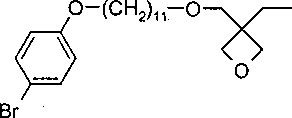
1,6
g (30 mmol) NaH wurden in 70 mL trockenem DMF suspendiert und unter
Schutzgas gerührt.
Dazu wurde bei 40 °C
eine Lösung
aus 6,8 g (20 mmol) 11-(4-Bromphenoxy)-1-undecanol
in 25 ml DMF gegeben. Nach 1h wurden 2,96 g (22 mmol) 3-Ethyl-3-(iodmethyl)oxetan
und 0,166g (1,0 mmol) Kl zugegeben und 24 h bei 40 °C gerührt. Nach
Abkühlen
auf Raumtemperatur wurde die Reaktionsmischung mit 200 mL Wasser
und 200 mL CH2Cl2 versetzt,
die organische Phase wurde abgetrennt, über Mg2SO4 getrocknet und das Lösungsmittel im Vakuum entfernt.
Das Produkt wurde chromatographisch gereinigt (Silica, Laufmittel
Hexan). Die Ausbeute betrug 3,2 g (89 % d. Th.), die Reinheit 98%
(nach HPLC).
1H-NMR (CDCl3,
500 MHz): 1,45 (t, J = 7,3 Hz, 3H), 1,45 (m, 14H), 1,55 (m, 2H),
1,75 (m, 4H), 3,42 (t, J = 6,3 Hz, 2H), 3,46 (s, 2,H), 3,85 (t,
J = 6,3 Hz, 2H), 4,39 (d, J = 5,9 Hz, 2H), 4,44 (d, J = 5,9 Hz,
2H), 6,75 (d, J = 9 Hz, 2H), 7,35 (d, J = 9 Hz, 2H).1.6 g (30 mmol) of NaH were suspended in 70 ml of dry DMF and stirred under protective gas. To At 40 ° C, a solution of 6.8 g (20 mmol) of 11- (4-bromophenoxy) -1-undecanol in 25 ml of DMF was added. After 1 h, 2.96 g (22 mmol) of 3-ethyl-3- (iodomethyl) oxetane and 0.166 g (1.0 mmol) of KI were added and stirred at 40 ° C for 24 h. After cooling to room temperature, 200 ml of water and 200 ml of CH 2 Cl 2 were added to the reaction mixture, the organic phase was separated off, dried over Mg 2 SO 4 and the solvent was removed in vacuo. The product was purified by chromatography (silica, eluent hexane). The yield was 3.2 g (89% of theory), the purity 98% (according to HPLC).
1 H-NMR (CDCl 3, 500 MHz): 1.45 (t, J = 7.3 Hz, 3H), 1.45 (m, 14H), 1.55 (m, 2H), 1.75 ( m, 4H), 3.42 (t, J = 6.3 Hz, 2H), 3.46 (s, 2, H), 3.85 (t, J = 6.3 Hz, 2H), 4, 39 (d, J = 5.9 Hz, 2H), 4.44 (d, J = 5.9 Hz, 2H), 6.75 (d, J = 9 Hz, 2H), 7.35 (d, J = 9 Hz, 2H).
e) Synthese von Oxetan-substituiertem N,N,N',N'-Tetraphenylbenzidine) Synthesis of oxetane-substituted N, N, N ', N'-tetraphenylbenzidine
Eine
entgaste Lösung
von 5,1 g (9,7 mmol) N,N'-Diphenylbenzidin
und 14 g (21,4 mmol) 3-(11-(4-Bromphenoxy)-undecan-1-oxy)methylen-3-ethyl-oxetan
in 250 mL 
Toluol
wurde 1 h mit N2 gesättigt. Dann wurde die Lösung zunächst mit
0,12 g (0,39 mmol) P(tBu)3, dann
mit 69 mg (0,19 mmol) Pd(OAc)2 versetzt.
Anschließend
wurden 3,8 g (50,4 mmol) festes NaOtBu zugegeben.
Die Reaktionsmischung wurde 5 h unter Rückfluss erhitzt. Nach Abkühlen auf
Raumtemperatur wurden 0,85 g NaCN und 10 mL Wasser zugesetzt. Die
organische Phase wurde mit 4 × 50
mL H2O gewaschen, über MgSO4 getrocknet
und die Lösungsmittel
in Vakuum entfernt. Das reine Produkt erhielt man durch Umkristallisation
aus Dioxan in einer Reinheit von 99,2% (gemäß HPLC). Die Ausbeute betrug
12 g (75% d. Th.).
1H-NMR (CDCl3, 500 MHz): 0,81 (t, J = 7,3 Hz, 6H), 1,17
(t, J = 7,0 Hz, 12H), 1,23-1,35
(m, 28H), 3,94 (t, J = 6,3 Hz, 4H), 4,03 (t, J = 6,3 Hz, 8H), 4,21
(d, J = 5,9 Hz, 4H), 4,29 (d, J = 5,9 Hz, 4H), 6,91-7,01 (m, 14H),
7,04 (d, J = 9 Hz, 4H), 7,27 (d, J = 8 Hz, 4H), 7,49 (d, J = 8,7
Hz, 4H).Toluene was saturated with N 2 for 1 h. Then, the solution was first treated with 0.12 g (0.39 mmol) of P ( t Bu) 3 , then with 69 mg (0.19 mmol) of Pd (OAc) 2 . Subsequently, 3.8 g (50.4 mmol) of solid NaO t Bu were added. The reaction mixture was refluxed for 5 hours. After cooling to room temperature, 0.85 g of NaCN and 10 mL of water were added. The organic phase was washed with 4 × 50 mL H 2 O, dried over MgSO 4 and the solvents removed in vacuo. The pure product was obtained by recrystallization from dioxane in a purity of 99.2% (according to HPLC). The yield was 12 g (75% of theory).
1 H-NMR (CDCl 3, 500 MHz): 0.81 (t, J = 7.3 Hz, 6H), 1.17 (t, J = 7.0 Hz, 12H), 1.23 to 1, 35 (m, 28H), 3.94 (t, J = 6.3 Hz, 4H), 4.03 (t, J = 6.3 Hz, 8H), 4.21 (d, J = 5.9 Hz, 4H), 4.29 (d, J = 5.9 Hz, 4H), 6.91-7.01 (m, 14H), 7.04 (d, J = 9 Hz, 4H), 7, 27 (d, J = 8Hz, 4H), 7.49 (d, J = 8.7Hz, 4H).
f)
Synthese von Oxetan-substituiertem, bromierten N,N,N',N'-Tetraphenylbenzidin
(Monomer M3) 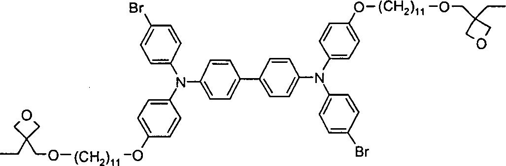
45,72
g (43,7 mmol) Oxetan-substituiertes N,N,N',N'-Tetraphenylbenzidin
wurden in 500 mL THF vorgelegt. Dazu wurde bei 0°C unter Lichtausschluss eine
Lösung
aus 15,15 g (84,4 mmol) NBS in 300 mL THF getropft. Man ließ auf RT
kommen und rührte
4 h weiter. Es wurden 500 mL Wasser zugesetzt, und die Mischung
wurde mit CH2Cl2 extrahiert.
Die organische Phase wurde über
MgSO4 getrocknet und die Lösungsmittel
in Vakuum entfernt. Das Produkt wurde mit Hexan heiß ausgerührt und
abgesaugt. Nach wiederholter chromatographischer Aufreinigung (Silica,
Hexan/Ethylacetat 4:1) erhielt man das Produkt in einer Ausbeute von
44 g (85 % d. Th.) als blassbraunes Öl, welches eine Reinheit von
99,2 % (gemäß HPLC)
aufwies.
1H-NMR (DMSO-d6,
500 MHz): 0,81 (t, J = 7,3 Hz, 6H), 1,17 (t, J = 7,0 Hz, 12H), 1,23-1,35
(m, 28H), 3,94 (t, J = 6,3 Hz, 4H), 4,03 (t, J = 6,3 Hz, 8H), 4,21
(d, J = 5,9 Hz, 4H), 4,29 (d, J = 5,9 Hz, 4H), 6,91-7,02 (m, 12H), 7,04
(d, J = 9 Hz, 4H), 7,29 (d, J = 8 Hz, 4H), 7,51 (d, J = 8,7 Hz,
4H).45.72 g (43.7 mmol) of oxetane-substituted N, N, N ', N'-tetraphenylbenzidine were initially charged in 500 ml of THF. For this purpose, a solution of 15.15 g (84.4 mmol) of NBS in 300 ml of THF was added dropwise at 0 ° C with the exclusion of light. It was allowed to come to RT and stirred for 4 h. 500 mL of water was added and the mixture was extracted with CH 2 Cl 2 . The organic phase was dried over MgSO 4 and the solvents removed in vacuo. The product was stirred hot with hexane and filtered with suction. After repeated chromatographic purification (silica, hexane / ethyl acetate 4: 1) the product was obtained in a yield of 44 g (85% of theory) as a pale brown oil which had a purity of 99.2% (according to HPLC).
1 H-NMR (DMSO-d 6 , 500 MHz): 0.81 (t, J = 7.3 Hz, 6H), 1.17 (t, J = 7.0 Hz, 12H), 1.23 1.35 (m, 28H), 3.94 (t, J = 6.3 Hz, 4H), 4.03 (t, J = 6.3 Hz, 8H), 4.21 (d, J = 5) , 9Hz, 4H), 4.29 (d, J = 5.9Hz, 4H), 6.91-7.02 (m, 12H), 7.04 (d, J = 9Hz, 4H), 7.29 (d, J = 8Hz, 4H), 7.51 (d, J = 8.7Hz, 4H).
g) Polymersynthese: Synthese von Polymer P1g) Polymer Synthesis: Synthesis of polymer P1
1,7056 g (2 mmol) Monomer M2, 0,9104 g (1,2 mmol) Monomer M1, 0,9723 g (0,8 mmol) Monomer M3 und 2,03 g (4,4 mmol) Kaliumphosphat-Hydrat wurden in 12,5 mL Toluol, 12,5 mL Dioxan und 12 mL Wasser (alle Lösungsmittel sauerstofffrei) gelöst und bei 40 °C 30 Minuten mit einem Argonstrom entgast. Dann wurden 0,90 mg Pd(OAc)2 und 6,30 mg P(o-tol)3 als Katalysator zugegeben, und die Reaktionsmischung wurde 3 h unter Rückfluss erhitzt. Es wurden 20 mL Toluol und als Endcapper 12 mg (0,04 mmol) 3,4-Bispentoxybenzolboronsäure zugegeben, 1 h unter Rückfluss erhitzt, dann wurden 20 mg (0,06 mmol) 3,4-Bispentoxybenzolbromid zugegeben und 1 h unter Rückfluss erhitzt. Die Reaktionslösung wurde auf 65°C abgekühlt und 4 h mit 10 mL 5%iger wässriger Natrium-N,N,Diethyldithiocarbamat-Lösung ausgerührt. Die organische Phase wurde mit 3 × 80 mL Wasser gewaschen und durch Zugabe in das doppelte Volumen Methanol ausgefällt. Das Rohpolymer wurde in Chlorbenzol gelöst, über Celit filtriert und durch Zugabe des doppelten Volumens Methanol gefällt. Man erhielt 2,24 g (78 d. Th.) des Polymers P1.1.7056 g (2 mmol) of monomer M2, 0.9104 g (1.2 mmol) of monomer M1, 0.9723 g (0.8 mmol) of monomer M3 and 2.03 g (4.4 mmol) of potassium phosphate hydrate were dissolved in 12.5 ml of toluene, 12.5 ml of dioxane and 12 ml of water (all solvents free of oxygen) and degassed at 40 ° C. for 30 minutes with an argon stream. Then, 0.90 mg of Pd (OAc) 2 and 6.30 mg of P (o-tol) 3 were added as a catalyst, and the reaction mixture was refluxed for 3 hours. 20 mL of toluene and, as endcapper, 12 mg (0.04 mmol) of 3,4-bispentoxy Benzoic acid added, heated under reflux for 1 h, then 20 mg (0.06 mmol) of 3,4-Bispentoxybenzolbromid were added and heated under reflux for 1 h. The reaction solution was cooled to 65 ° C and stirred for 4 h with 10 mL of 5% aqueous sodium N, N, diethyldithiocarbamate solution. The organic phase was washed with 3 x 80 mL of water and precipitated by addition to twice the volume of methanol. The crude polymer was dissolved in chlorobenzene, filtered through Celite and precipitated by adding twice the volume of methanol. This gave 2.24 g (78 d.th.) of the polymer P1.
Beispiel 2: Synthese eines kationisch vernetzbaren Polymers P2 für die Verwendung als Pufferschicht Example 2: Synthesis of a cationically crosslinkable polymer P2 for use as a buffer layer
a)
Synthese von Bis-(4-bromphenyl)-(4-secbutylphenyl)-amin
(Monomer M4) 
Die
Synthese von Monomer M4 wurde in Analogie zur Synthese in
b)
Synthese von Bis-((4-boronsäurepinakolester)phenyl)-(4-secbutylphenyl)-amin (Monomer M5) 
Die
Synthese von Monomer M5 ist beschrieben in der nicht offen gelegten
Anmeldung
c)
Synthese von 2,7-Dibrom-(2,5-dimethylphenyl)-9-(3,4-di(3-ethyl(oxetan-3-ethyloxy)-hexyloxyphenyl))-fluoren
(Monomer M6) 
Die Synthese von Monomer M6 ist beschrieben in C. D. Müller et al., Nature 2003, 421, 829.The Synthesis of monomer M6 is described in C. D. Müller et al., Nature 2003, 421, 829.
d) Polymersynthese: Synthese von Polymer P2 d) Polymer Synthesis: Synthesis of polymer P2
1,4695 g (3,2 mmol) Monomer M4, 2,2134 g (4 mmol) Monomer M5, 0,7463 g (0,8 mmol) Monomer M6 und 4,05 g (8,8 mmol) Kaliumphosphat-Hydrat wurden in 25 mL Toluol, 25 mL Dioxan und 25 mL Wasser (alle Lösungsmittel sauerstofffrei) gelöst und bei 40°C 30 Minuten mit einem Argonstrom entgast. Dann wurden 1,80 mg Pd(OAc)2 und 14,61 mg P(o-tol)3 als Katalysator zugegeben, und die Reaktionsmischung wurde 10 h unter Rückfluss erhitzt. Dabei wurden nach 4 h, nach 5,5 h und nach 8,5 h jeweils die Ausgangsmenge an Pd(OAc)2 und P(o-tol)3 zugegeben. Nach 8 h Reaktionszeit wurden 2 mL Toluol zugegeben. Als Endcapper wurden 24 mg (0,08 mmol) 3,4-Bispentoxybenzolboronsäure zugegeben, 2 h unter Rückfluss erhitzt, dann wurden 40 mg (0,12 mmol) 3,4-Bispentoxybenzolbromid zugegeben und 1 h unter Rückfluss erhitzt. Die Reaktionslösung wurde auf 65 °C abgekühlt und 4 h mit 20 mL 5 %iger wässriger Lösung von Natrium-N,N-Diethyldithiocarbamat ausgerührt. Die Phasen wurden getrennt und der Vorgang wurde noch einmal mit 40 mL der Dithiocarbamat-Lösung wiederholt. Die Phasen wurden getrennt, die organische Phase mit 3 × 150 mL Wasser gewaschen und durch Zugabe in das doppelte Volumen Methanol ausgefällt. Das Rohpolymer wurde in Chlorbenzol gelöst, über Celit filtriert und durch Zugabe des doppelten Volumens Methanol gefällt. Man erhielt 1,84 g (64% d. Th.) des Polymers P2, das in Chlorbenzol löslich, jedoch in Toluol, THF oder Chloroform unlöslich ist.1.4695 g (3.2 mmol) of M4 monomer, 2.2134 g (4 mmol) of M5 monomer, 0.7463 g (0.8 mmol) of M6 monomer, and 4.05 g (8.8 mmol) of potassium phosphate hydrate were dissolved in 25 ml of toluene, 25 ml of dioxane and 25 ml of water (all solvents free of oxygen) and degassed at 40 ° C. for 30 minutes with an argon stream. Then, 1.80 mg of Pd (OAc) 2 and 14.61 mg of P (o-tol) 3 were added as a catalyst, and the reaction mixture was refluxed for 10 hours. The starting amount of Pd (OAc) 2 and P (o-tol) 3 were added after 4 h, after 5.5 h and after 8.5 h. After a reaction time of 8 h, 2 ml of toluene were added. 24 mg (0.08 mmol) of 3,4-bispentoxybenzeneboronic acid were added as the end capper and heated under reflux for 2 h, then 40 mg (0.12 mmol) of 3,4-bispentoxybenzene bromide were added and the mixture was refluxed for 1 h. The re reaction solution was cooled to 65 ° C and stirred for 4 h with 20 mL of 5% aqueous solution of sodium N, N-Diethyldithiocarbamat. The phases were separated and the process was repeated once more with 40 mL of the dithiocarbamate solution. The phases were separated, the organic phase was washed with 3 × 150 ml of water and precipitated by adding it to twice the volume of methanol. The crude polymer was dissolved in chlorobenzene, filtered through Celite and precipitated by adding twice the volume of methanol. This gave 1.84 g (64% of theory) of the polymer P2, which is soluble in chlorobenzene but insoluble in toluene, THF or chloroform.
Beispiel
3: Synthese eines kationisch vernetzbaren Moleküls V1 für die Verwendung als Pufferschicht 
Die Synthese des kationisch vernetzbaren Moleküls V1 ist beschrieben in M. S. Bayer et al., Macromol. Rapid Commun. 1999, 20, 224–228.The Synthesis of the cationically crosslinkable molecule V1 is described in M. Bayer et al., Macromol. Rapid Commun. 1999, 20, 224-228.
Die Deviceergebnisse, die bei Verwendung des Polymers P1 und P2 bzw. des Moleküls V1 als Pufferschicht erhalten wurden, sind in Beispiel 6–8 zusammengefasst.The Device results obtained when using the polymer P1 and P2 or of the molecule V1 as a buffer layer are summarized in Example 6-8.
Beispiel 4: Herstellung von LEDs mit einer zusätzlichen PufferschichtExample 4: Preparation of LEDs with an additional buffer layer
Die
Herstellung von LEDs erfolgte nach einem allgemeinen Verfahren,
welches im Einzelfall auf die jeweiligen Gegebenheiten (z. B. Lösungsviskosität und optimale
Schichtdicke der funktionellen Schichten im Device) angepasst wurde.
Die im Nachfolgenden beschriebenen LEDs waren jeweils Dreischichtsysteme,
d. h. Substrat//ITO//PEDOT//Pufferschicht//Polymer//Kathode. PEDOT
ist ein Polythiophen-Derivat (Baytron P4083 von H. C. Stark, Goslar).
Als Kathode wurde in allen Fällen
Ba von der Firma Aldrich und Ag von der Firma Aldrich verwendet.
Wie PLEDs allgemein dargestellt werden können, ist bereits in
Davon
abweichend wurde hier auf die PEDOT-Schicht ein kationisch vernetzbarer
Halbleiter als Pufferschicht aufgebracht. Als Materialien für die Pufferschicht
wurden hier die vernetzbaren Polymere P1 und P2 bzw. die vernetzbare
niedermolekulare Verbindung V1 verwendet. Von dem vernetzbaren Material
wird eine Lösung
(in der Regel mit einer Konzentration von 4–25 mg/ml in beispielsweise
Toluol, Chlorbenzol, Xylol etc.) angesetzt und durch Rühren bei
Raumtemperatur gelöst.
Je nach Material kann es auch vorteilhaft sein, für einige
Zeit bei 50–70 °C zu rühren. Hat
sich die Verbindung vollständig
gelöst,
wird sie durch einen 5 μm
Filter filtriert. Dann wird die Pufferschicht bei variablen Geschwindigkeiten
(400–6000
rpm) mit einem Spincoater in einer inerten Atmosphäre aufgeschleudert.
Die Schichtdicken können
dadurch im Bereich von ca. 20 und 300 nm variiert werden. Anschließend erfolgt
die Vernetzung durch Erhitzen des Devices auf 180°C für 30 Minuten auf
einer Heizplatte in einer iterten Atmosphäre. Auf die Pufferschicht werden
nun der organische Halbleiter und die Kathode aufgebracht, wie in
Beispiel 5: Herstellung von strukturierten LEDs mit einer zusätzlichen PufferschichtExample 5: Preparation of structured LEDs with an additional buffer layer
Die Herstellung der strukturierten LEDs erfolgt zunächst analog zu Beispiel 4 bis einschließlich zum Schritt der Vernetzung der Pufferschicht. Abweichend dazu werden als organische Halbleiter mehrere kationisch vernetzbare Halbleiter verwendet. Als kationisch vernetzbare Halbleiter wurden rot, grün und blau emittierende konjugierte Polymere auf Basis von Poly-Spirobifluoren verwendet, die mit Oxetangruppen funktionalisiert wurden. Diese Materialien und deren Synthese wurden bereits in der Literatur beschrieben (Nature 2003, 421, 829). Von den kationisch vernetzbaren Halbleitern wird eine Lösung (in der Regel mit einer Konzentration von 4–25 mg/ml in beispielsweise Toluol, Chlorbenzol, Xylol:Cyclohexanon (4:1)) angesetzt und durch Rühren bei Raumtemperatur gelöst. Je nach Verbindung kann es auch vorteilhaft sein, für einige Zeit bei 50–70°C zu rühren. Dabei werden den Lösungen des kationisch vernetzbaren Halbleiters noch ca. 0,5 Gew.% (bezogen auf das Polymer) einer Photosäure (hier: {4-[(2-hydroxytetradecyl)-oxyl]-phenyl}-phenyliodonium hexafluoroantimonat) zugesetzt. Auf die vernetzte Pufferschicht wird nun durch Spincoating unter vergleichbaren Bedingungen wie für die Pufferschicht die Lösung des ersten kationisch vernetzbaren Halbleiters und der Photosäure aufgebracht. Nach Trocknen des Films wird durch Bestrahlung mit einer UV Lampe (10 W, 302 nm, 5 Min.) durch eine Maske strukturiert vernetzt. Der Film wird dann unter einer interten Atmosphäre 3 Minuten bei 130°C getempert, anschließend mit einer 10–4-molaren LiAlH4-Lösung in THF behandelt und mit THF nachgespült. Dadurch werden die nicht-vernetzten Stellen im Film abgewaschen. Dieser Vorgang wird mit den weiteren Lösungen der vernetzbaren organischen Halbleiter wiederholt, und auf diese Weise werden die drei Grundfarben strukturiert nebeneinander aufgebracht. Das Aufdampfen der Elektroden und die Kontaktierung erfolgen dann, wie oben beschrieben.The production of the structured LEDs is initially carried out analogously to Example 4 through to the step of crosslinking the buffer layer. Deviating from this, several cationically crosslinkable semiconductors are used as organic semiconductors. As cationically crosslinkable semiconductors, red, green, and blue-emitting conjugated polymers based on poly-spirobifluorene functionalized with oxetane groups have been used. These materials and their synthesis have already been described in the literature (Nature 2003, 421, 829). Of the cationically crosslinkable semiconductors, a solution (usually with a concentration of 4-25 mg / ml in, for example, toluene, chlorobenzene, xylene: cyclohexanone (4: 1)) is prepared and dissolved by stirring at room temperature. Depending on the compound, it may also be advantageous to stir at 50-70 ° C for some time. About 0.5% by weight (based on the polymer) of a photoacid (here: {4 - [(2-hydroxytetradecyl) -oxyl] -phenyl} -phenyl-iodonium hexafluoroantimonate) is added to the solutions of the cationically crosslinkable semiconductor. The crosslinked buffer layer is now spincoated under comparable conditions As for the buffer layer, the solution of the first cationic crosslinkable semiconductor and the photoacid applied. After drying the film is crosslinked by irradiation with a UV lamp (10 W, 302 nm, 5 min.) Structured through a mask. The film is then annealed under an inert atmosphere for 3 minutes at 130 ° C, then treated with a 10 -4 molar LiAlH 4 solution in THF and rinsed with THF. This will wash away the non-crosslinked areas in the film. This process is repeated with the other solutions of the crosslinkable organic semiconductors, and in this way the three primary colors are applied next to each other in a structured manner. The vapor deposition of the electrodes and the contacting are then carried out as described above.
Beispiel 6: Lebensdauermessung einer LED mit einer zusätzlichen Pufferschicht P1Example 6: Lifetime measurement an LED with an additional Buffer layer P1
Die LED wurde hergestellt, wie in Beispiel 4 beschrieben. Dabei wurden 20 nm PEDOT verwendet. Als Pufferschicht wurde eine 20 nm dicke Schicht von Polymer P1 aufgebracht, die wie in Beispiel 4 beschrieben thermisch vernetzt wurde. Als halbleitendes Polymer wurde ein blau emittierendes Polymer verwendet, das 50 mol% Monomer M7, 30 mol% Monomer M8, 10 mol% Monomer M1 und 10 mol% Monomer M9 enthielt. Die Monomere sind unten abgebildet, ihre Synthese ist beschrieben in WO 03/020790. Das Polymer zeigte in der Elektrolumineszenz eine Lebensdauer (= Helligkeitsabfall auf die Hälfte der Anfangshelligkeit) von ca. 1600 h bei Raumtemperatur und einer Anfangshelligkeit von 300 cd/m2. In einer Vergleichs-LED ohne die Pufferschicht zeigte das Polymer unter ansonsten gleichen Bedingungen eine Lebensdauer von ca. 500 h. Es wurde außerdem eine LED hergestellt, deren Pufferschicht unter Zusatz von 0,5 Gew.% {4-[(2-hydroxytetradecyl)-oxyl]-phenyl}-phenyliodonium hexafluoroantimonat photochemisch durch UV-Bestrahlung (3 s, 302 nm) und anschließendes Erhitzen auf 90°C für 30 Sekunden vernetzt wurde. Die Pufferschicht wurde anschließend mit THF gespült und 5 Minuten auf 180°C erhitzt. Diese LED hatte unter ansonsten gleichen Bedingungen eine Lebensdauer von ca. 630 h.The LED was prepared as described in Example 4. In this case 20 nm PEDOT were used. As a buffer layer, a 20 nm thick layer of polymer P1 was applied, which was thermally crosslinked as described in Example 4. As the semiconductive polymer, a blue-emitting polymer containing 50 mol% of monomer M7, 30 mol% of monomer M8, 10 mol% of monomer M1 and 10 mol% of monomer M9 was used. The monomers are shown below, their synthesis is described in WO 03/020790. The polymer showed in electroluminescence a lifetime (= brightness drop to half the initial brightness) of about 1600 h at room temperature and an initial brightness of 300 cd / m 2 . In a comparative LED without the buffer layer, the polymer showed a life of about 500 h under otherwise identical conditions. In addition, an LED was prepared whose buffer layer with the addition of 0.5% by weight of {4 - [(2-hydroxytetradecyl) -oxyl] -phenyl} -phenyl-iodonium hexafluoroantimonate was photochemically UV-irradiated (3 s, 302 nm) and then Heating was cured at 90 ° C for 30 seconds. The buffer layer was then rinsed with THF and heated to 180 ° C for 5 minutes. This LED had a lifetime of approximately 630 h under otherwise identical conditions.
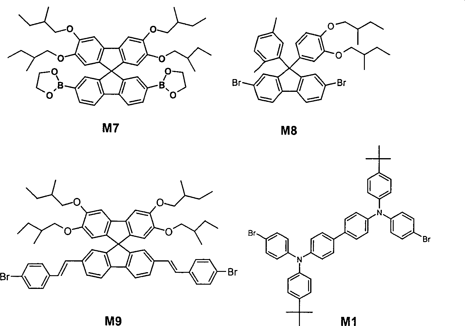
Beispiel 7: Lebensdauermessung einer LED mit einer zusätzlichen Pufferschicht P2Example 7: Lifetime measurement an LED with an additional Buffer layer P2
Die Messung wurde wiederholt mit Polymer P2 als Pufferschicht, wie in Beispiel 6 beschrieben unter ansonsten identischen Bedingungen. Das Polymer zeigte eine Lebensdauer von ca. 1500 h ohne Zusatz von Photosäure zur Pufferschicht und von ca. 600 h mit Zusatz von Photosäure.The Measurement was repeated with polymer P2 as buffer layer as in Example 6 described under otherwise identical conditions. The polymer showed a lifetime of about 1500 h without the addition of photoacid for Buffer layer and about 600 h with addition of photoacid.
Beispiel 8: Lebensdauermessung einer LED mit einer zusätzlichen Pufferschicht V1Example 8: Lifetime measurement an LED with an additional Buffer layer V1
Die Messung wurde wiederholt mit Verbindung V1 als Pufferschicht, wie in Beispiel 6 beschrieben unter ansonsten identischen Bedingungen. Das Polymer zeigte eine Lebensdauer von ca. 1350 h ohne Zusatz von Photosäure zur Pufferschicht und von ca. 550 h mit Zusatz von Photosäure.The Measurement was repeated with compound V1 as a buffer layer, such as in Example 6 under otherwise identical conditions. The polymer showed a life of about 1350 h without the addition of Photo acid to the buffer layer and from about 550 h with the addition of photoacid.
Claims (24)

Priority Applications (18)
| Application Number | Priority Date | Filing Date | Title |
|---|---|---|---|
| DE2003140711 DE10340711A1 (en) | 2003-09-04 | 2003-09-04 | Electronic device containing organic semiconductors |
| DE200450012028 DE502004012028D1 (en) | 2003-09-04 | 2004-09-04 | ELECTRONIC DEVICE CONTAINING AN ORGANIC LADDER AND AN ORGANIC SEMICONDUCTOR AND BETWEEN A BUFFER LAYER CONSISTING OF A POLYMER WHICH IS CATIONICALLY POLYMERIZABLE |
| JP2006525128A JP5133562B2 (en) | 2003-09-04 | 2004-09-04 | Electronic devices including organic semiconductors |
| CNB2004800289980A CN100508237C (en) | 2003-09-04 | 2004-09-04 | Electronic devices comprising an organic conductor and semiconductor as well as an intermediate buffer layer made of a crosslinked polymer |
| EP20040764854 EP1661191B1 (en) | 2003-09-04 | 2004-09-04 | Electronic devices comprising an organic conductor and semiconductor as well as an intermediate buffer layer made of a crosslinked polymer |
| US10/570,372 US7901766B2 (en) | 2003-09-04 | 2004-09-04 | Electronic devices comprising an organic conductor and semiconductor as well as an intermediate buffer layer made of a crosslinked polymer |
| EP04764853.0A EP1671379B2 (en) | 2003-09-04 | 2004-09-04 | Electronic device comprising an organic semiconductor, an organic semiconductor, and an intermediate buffer layer made of a polymer that is cationically polymerizable |
| PCT/EP2004/009903 WO2005024971A1 (en) | 2003-09-04 | 2004-09-04 | Electronic devices comprising an organic conductor and semiconductor as well as an intermediate buffer layer made of a crosslinked polymer |
| PCT/EP2004/009902 WO2005024970A1 (en) | 2003-09-04 | 2004-09-04 | Electronic device comprising an organic semiconductor, an organic semiconductor, and an intermediate buffer layer made of a polymer that is cationically polymerizable and contains no photoacid |
| KR1020067004566A KR101042863B1 (en) | 2003-09-04 | 2004-09-04 | Electronic devices comprising an organic conductor and semiconductor and an intermediate buffer layer of a crosslinked polymer |
| US10/570,640 US20070034862A1 (en) | 2003-09-04 | 2004-09-04 | Electronic device comprising an organic semiconductor, an organic semiconductor, and an intermediate buffer layer made of a polymer that is cationically polymerizable and contains no photoacid |
| AT04764853T ATE492913T1 (en) | 2003-09-04 | 2004-09-04 | ELECTRONIC DEVICE CONTAINING AN ORGANIC CONDUCTOR AND AN ORGANIC SEMICONDUCTOR AND IN BETWEEN A BUFFER LAYER CONSISTING OF A POLYMER WHICH CAN BE CATIONICALLY POLYMERIZED |
| CNA2004800253688A CN1849717A (en) | 2003-09-04 | 2004-09-04 | Electronic devices comprising an organic conductor and semiconductor as well as an intermediate buffer layer made of a crosslinked polymer |
| DE200450008698 DE502004008698D1 (en) | 2003-09-04 | 2004-09-04 | ELECTRONIC DEVICES CONTAINING AN ORGANIC LADDER AND SEMICONDUCTOR AND BETWEEN A BUFFER LAYER OF A NETWORKED POLYMER |
| JP2006525129A JP5355857B2 (en) | 2003-09-04 | 2004-09-04 | An electronic device comprising an organic conductor and a semiconductor and an intermediate buffer layer made of a crosslinked polymer |
| AT04764854T ATE418161T1 (en) | 2003-09-04 | 2004-09-04 | ELECTRONIC DEVICES CONTAINING AN ORGANIC CONDUCTOR AND SEMICONDUCTOR AND A BUFFER LAYER MADE OF A CROSS-LINKED POLYMER IN BETWEEN |
| KR1020067004561A KR101071034B1 (en) | 2003-09-04 | 2006-03-03 | Electronic Devices Containing Organic Semiconductors |
| JP2013098569A JP2013191867A (en) | 2003-09-04 | 2013-05-08 | Electronic devices comprising organic conductor and semiconductor and intermediate buffer layer made of crosslinked polymer |
Applications Claiming Priority (1)
| Application Number | Priority Date | Filing Date | Title |
|---|---|---|---|
| DE2003140711 DE10340711A1 (en) | 2003-09-04 | 2003-09-04 | Electronic device containing organic semiconductors |
Publications (1)
| Publication Number | Publication Date |
|---|---|
| DE10340711A1 true DE10340711A1 (en) | 2005-04-07 |
Family
ID=34258390
Family Applications (3)
| Application Number | Title | Priority Date | Filing Date |
|---|---|---|---|
| DE2003140711 Withdrawn DE10340711A1 (en) | 2003-09-04 | 2003-09-04 | Electronic device containing organic semiconductors |
| DE200450012028 Active DE502004012028D1 (en) | 2003-09-04 | 2004-09-04 | ELECTRONIC DEVICE CONTAINING AN ORGANIC LADDER AND AN ORGANIC SEMICONDUCTOR AND BETWEEN A BUFFER LAYER CONSISTING OF A POLYMER WHICH IS CATIONICALLY POLYMERIZABLE |
| DE200450008698 Active DE502004008698D1 (en) | 2003-09-04 | 2004-09-04 | ELECTRONIC DEVICES CONTAINING AN ORGANIC LADDER AND SEMICONDUCTOR AND BETWEEN A BUFFER LAYER OF A NETWORKED POLYMER |
Family Applications After (2)
| Application Number | Title | Priority Date | Filing Date |
|---|---|---|---|
| DE200450012028 Active DE502004012028D1 (en) | 2003-09-04 | 2004-09-04 | ELECTRONIC DEVICE CONTAINING AN ORGANIC LADDER AND AN ORGANIC SEMICONDUCTOR AND BETWEEN A BUFFER LAYER CONSISTING OF A POLYMER WHICH IS CATIONICALLY POLYMERIZABLE |
| DE200450008698 Active DE502004008698D1 (en) | 2003-09-04 | 2004-09-04 | ELECTRONIC DEVICES CONTAINING AN ORGANIC LADDER AND SEMICONDUCTOR AND BETWEEN A BUFFER LAYER OF A NETWORKED POLYMER |
Country Status (8)
| Country | Link |
|---|---|
| US (2) | US7901766B2 (en) |
| EP (2) | EP1661191B1 (en) |
| JP (3) | JP5355857B2 (en) |
| KR (2) | KR101042863B1 (en) |
| CN (2) | CN100508237C (en) |
| AT (2) | ATE418161T1 (en) |
| DE (3) | DE10340711A1 (en) |
| WO (2) | WO2005024970A1 (en) |
Cited By (1)
| Publication number | Priority date | Publication date | Assignee | Title |
|---|---|---|---|---|
| US7608856B2 (en) | 2004-05-03 | 2009-10-27 | Merck Patent Gmbh | Electronic devices comprising organic semiconductors |
Families Citing this family (47)
| Publication number | Priority date | Publication date | Assignee | Title |
|---|---|---|---|---|
| DE10340711A1 (en) * | 2003-09-04 | 2005-04-07 | Covion Organic Semiconductors Gmbh | Electronic device containing organic semiconductors |
| KR100738219B1 (en) * | 2003-12-23 | 2007-07-12 | 삼성에스디아이 주식회사 | Substance for Intermediate layer of organic electroluminescent device and organic electroluminescent device using the same |
| GB2425654B (en) * | 2005-04-29 | 2010-03-17 | Seiko Epson Corp | A method of fabricating a heterojunction of organic semiconducting polymers |
| KR100715548B1 (en) * | 2005-07-29 | 2007-05-07 | 광 석 서 | Conducting Polymer Synthesized with Partially Substituted Polymers as a Dopant |
| US7576356B2 (en) * | 2005-08-08 | 2009-08-18 | Osram Opto Semiconductors Gmbh | Solution processed crosslinkable hole injection and hole transport polymers for OLEDs |
| US8440324B2 (en) * | 2005-12-27 | 2013-05-14 | E I Du Pont De Nemours And Company | Compositions comprising novel copolymers and electronic devices made with such compositions |
| EP2412699A1 (en) * | 2005-12-28 | 2012-02-01 | E.I. Du Pont De Nemours And Company | Compositions comprising novel compounds and electronic devices made with such compositions |
| US8138075B1 (en) | 2006-02-06 | 2012-03-20 | Eberlein Dietmar C | Systems and methods for the manufacture of flat panel devices |
| DE102006006412A1 (en) * | 2006-02-13 | 2007-08-16 | Merck Patent Gmbh | Electronic component, process for its production and its use |
| CN101443928A (en) | 2006-05-12 | 2009-05-27 | 默克专利有限公司 | Indenofluorene polymer based organic semiconductor materials |
| JP4175397B2 (en) * | 2006-06-28 | 2008-11-05 | セイコーエプソン株式会社 | Method for manufacturing organic electroluminescent device |
| WO2008010487A1 (en) | 2006-07-19 | 2008-01-24 | Hitachi Chemical Co., Ltd. | Organic electronic material, organic electronic device and organic electroluminescent device |
| US8222807B2 (en) * | 2007-02-15 | 2012-07-17 | Mitsubishi Chemical Corporation | Organic electroluminescence device and method of producing organic device |
| JP5196928B2 (en) | 2007-09-18 | 2013-05-15 | キヤノン株式会社 | Organic light emitting device and display device |
| US8586684B2 (en) | 2007-11-21 | 2013-11-19 | Merck Patent Gmbh | Conjugated copolymer |
| US20090236979A1 (en) * | 2008-03-24 | 2009-09-24 | Air Products And Chemicals, Inc. | Organic Electroluminescent Device and the Method of Making |
| JP5540600B2 (en) * | 2008-08-13 | 2014-07-02 | 三菱化学株式会社 | Electronic device, organic electroluminescent element, organic EL display device, and organic EL lighting |
| US8643000B2 (en) * | 2008-11-18 | 2014-02-04 | E I Du Pont De Nemours And Company | Organic electronic device with low-reflectance electrode |
| JP5359255B2 (en) * | 2008-12-19 | 2013-12-04 | コニカミノルタ株式会社 | Organic photoelectric conversion element |
| JP5141600B2 (en) * | 2009-03-09 | 2013-02-13 | 三菱化学株式会社 | Method for producing composition for organic electroluminescent device |
| CN101624589B (en) * | 2009-04-10 | 2011-08-31 | 重庆大学 | Novel Rhizopus oryzae immobilized fermentation carrier unit and use method |
| WO2010140553A1 (en) * | 2009-06-01 | 2010-12-09 | 日立化成工業株式会社 | Organic electronic material, ink composition containing same, and organic thin film, organic electronic element, organic electroluminescent element, lighting device, and display device formed therewith |
| CA2786713C (en) * | 2010-01-19 | 2018-03-06 | Sirigen Group Limited | Novel reagents for directed biomarker signal amplification |
| US8859171B2 (en) * | 2010-03-03 | 2014-10-14 | Xerox Corporation | Charge transport particles |
| KR101181228B1 (en) * | 2010-10-11 | 2012-09-10 | 포항공과대학교 산학협력단 | Organic solar cell and method for preparing the same |
| KR101756657B1 (en) * | 2010-11-03 | 2017-07-12 | 엘지디스플레이 주식회사 | White organic light emitting device and display device using the same |
| JP5944120B2 (en) * | 2011-07-21 | 2016-07-05 | コニカミノルタ株式会社 | ORGANIC PHOTOELECTRIC CONVERSION DEVICE, ITS MANUFACTURING METHOD, AND ORGANIC SOLAR CELL USING THE SAME |
| JPWO2014038559A1 (en) * | 2012-09-04 | 2016-08-12 | 三菱化学株式会社 | Organic electroluminescent device and manufacturing method thereof |
| US9502657B2 (en) | 2012-09-07 | 2016-11-22 | Pioneer Corporation | Organic electroluminescence device and manufacturing method thereof |
| US9478765B2 (en) | 2012-09-18 | 2016-10-25 | Nederlandse Organisatie Voor Toegepast-Natuurwetenschappelijk Onderzoek Tno | Electro-optical device stack, having patches covering layer breaches |
| US10003024B2 (en) * | 2012-09-27 | 2018-06-19 | Merck Patent Gmbh | Materials for organic electroluminescent devices |
| JP6371304B2 (en) * | 2012-12-13 | 2018-08-08 | イー・アイ・デュポン・ドウ・ヌムール・アンド・カンパニーE.I.Du Pont De Nemours And Company | Confinement layer and methods and materials for manufacturing devices manufactured using the same |
| JP6648692B2 (en) * | 2014-03-27 | 2020-02-14 | 日産化学株式会社 | Charge transporting varnish |
| JP6610536B2 (en) * | 2014-04-09 | 2019-11-27 | 住友化学株式会社 | Light emitting device and composition used therefor |
| WO2016136847A1 (en) * | 2015-02-25 | 2016-09-01 | 三菱化学株式会社 | Polymer, composition for organic electroluminescent element, organic electroluminescent element, organic el display device, and organic el illumination |
| JP2018532269A (en) * | 2015-10-16 | 2018-11-01 | ダウ グローバル テクノロジーズ エルエルシー | Process for making organic charge transport membranes |
| US9644112B1 (en) * | 2016-04-20 | 2017-05-09 | Eastman Kodak Company | Articles having electrically-conductive layer or pattern |
| US10892414B2 (en) | 2016-12-06 | 2021-01-12 | Merck Patent Gmbh | Process for making electronic device |
| JP7056644B2 (en) * | 2017-03-24 | 2022-04-19 | 日産化学株式会社 | Fluorine atom-containing polymer and its utilization |
| JP2018203889A (en) * | 2017-06-06 | 2018-12-27 | 日立化成株式会社 | Curable polymer, polymerization liquid, conductive film and organic light-emitting element |
| WO2019009327A1 (en) * | 2017-07-04 | 2019-01-10 | 日立化成株式会社 | Organic electronics material and organic electronics element |
| KR102385225B1 (en) | 2017-07-12 | 2022-04-11 | 삼성디스플레이 주식회사 | Composition for fabricating organic film, display device using the same and method for manufacturing the display device |
| CN107799571B (en) * | 2017-10-12 | 2020-10-09 | 武汉华星光电半导体显示技术有限公司 | Organic light emitting diode device and display device |
| WO2020011701A1 (en) * | 2018-07-11 | 2020-01-16 | Merck Patent Gmbh | Formulation containing a highly branched polymer, highly branched polymer and electro-optical device containing this highly branched polymer |
| KR20200069400A (en) | 2018-12-05 | 2020-06-17 | 삼성디스플레이 주식회사 | Condensed ring compound, composition including the same and organic light-emitting device including thin film formed therefrom |
| KR20220036393A (en) | 2020-09-14 | 2022-03-23 | 삼성디스플레이 주식회사 | Display device |
| KR20220060630A (en) | 2020-11-04 | 2022-05-12 | 삼성디스플레이 주식회사 | Conductive bonding structure for boards and display device including the same |
Family Cites Families (52)
| Publication number | Priority date | Publication date | Assignee | Title |
|---|---|---|---|---|
| US4720432A (en) | 1987-02-11 | 1988-01-19 | Eastman Kodak Company | Electroluminescent device with organic luminescent medium |
| US5331183A (en) | 1992-08-17 | 1994-07-19 | The Regents Of The University Of California | Conjugated polymer - acceptor heterojunctions; diodes, photodiodes, and photovoltaic cells |
| JP3082479B2 (en) * | 1992-10-23 | 2000-08-28 | ジェイエスアール株式会社 | Negative radiation-sensitive resin composition |
| DE4325885A1 (en) * | 1993-08-02 | 1995-02-09 | Basf Ag | Electroluminescent arrangement |
| JP2848207B2 (en) | 1993-09-17 | 1999-01-20 | 凸版印刷株式会社 | Organic thin film EL device |
| EP0666298A3 (en) | 1994-02-08 | 1995-11-15 | Tdk Corp | Organic EL element and compound used therein. |
| EP0676461B1 (en) | 1994-04-07 | 2002-08-14 | Covion Organic Semiconductors GmbH | Spiro compounds and their application as electroluminescence materials |
| CN1106696C (en) | 1994-05-16 | 2003-04-23 | 皇家菲利浦电子有限公司 | Semiconductor device provided with organic semiconductor material |
| JP3246189B2 (en) | 1994-06-28 | 2002-01-15 | 株式会社日立製作所 | Semiconductor display device |
| TW293172B (en) | 1994-12-09 | 1996-12-11 | At & T Corp | |
| DE19500912A1 (en) * | 1995-01-13 | 1996-07-18 | Basf Ag | Electroluminescent arrangement |
| KR100431015B1 (en) * | 1995-07-28 | 2004-07-30 | 다우 글로벌 테크놀로지스 인크. | 2,7-aryl-9-substituted fluorenes and 9-substituted fluorene oligomers and polymers |
| CN1229415C (en) * | 1995-07-28 | 2005-11-30 | 陶氏环球技术公司 | 2,7-aryl-9-substituted fluorenes and 9-substituted fluorene oligomers and polymers |
| US5929194A (en) † | 1996-02-23 | 1999-07-27 | The Dow Chemical Company | Crosslinkable or chain extendable polyarylpolyamines and films thereof |
| JP3643433B2 (en) † | 1996-03-25 | 2005-04-27 | ケミプロ化成株式会社 | Triphenylamine-containing polyetherketone, process for producing the same, and organic EL device using the same |
| WO1998003566A1 (en) | 1996-07-19 | 1998-01-29 | The Regents Of The University Of California | Conjugated polymers as materials for solid state lasers |
| JP3899566B2 (en) | 1996-11-25 | 2007-03-28 | セイコーエプソン株式会社 | Manufacturing method of organic EL display device |
| DE19652261A1 (en) | 1996-12-16 | 1998-06-18 | Hoechst Ag | Aryl-substituted poly (p-arylenevinylenes), process for their preparation and their use in electroluminescent devices |
| DE19711713A1 (en) | 1997-03-20 | 1998-10-01 | Hoechst Ag | Photovoltaic cell |
| US6309763B1 (en) * | 1997-05-21 | 2001-10-30 | The Dow Chemical Company | Fluorene-containing polymers and electroluminescent devices therefrom |
| WO1999010939A2 (en) | 1997-08-22 | 1999-03-04 | Koninklijke Philips Electronics N.V. | A method of manufacturing a field-effect transistor substantially consisting of organic materials |
| JP2000077185A (en) * | 1998-08-28 | 2000-03-14 | Asahi Chem Ind Co Ltd | Organic electroluminescent element |
| US6107452A (en) * | 1998-10-09 | 2000-08-22 | International Business Machines Corporation | Thermally and/or photochemically crosslinked electroactive polymers in the manufacture of opto-electronic devices |
| KR100400291B1 (en) * | 1998-11-27 | 2004-02-05 | 주식회사 하이닉스반도체 | Novel photoresist monomer, polymer thereof and photoresist composition using the same |
| KR100766288B1 (en) | 1999-01-15 | 2007-10-11 | 스미또모 가가꾸 가부시키가이샤 | Semiconducting polymer field effect transistor |
| JP2001076874A (en) * | 1999-09-07 | 2001-03-23 | Tdk Corp | Organic el display device |
| KR20020095210A (en) * | 2000-04-11 | 2002-12-20 | 듀폰 디스플레이즈, 인크. | Soluble Poly(aryl-oxadiazole) Conjugated Polymers |
| DE10037391A1 (en) * | 2000-08-01 | 2002-02-14 | Covion Organic Semiconductors | Structurable materials, processes for their production and their use |
| DE10044840A1 (en) * | 2000-09-11 | 2002-04-04 | Siemens Ag | Photostructurable new organic semiconductor materials |
| CN100357370C (en) | 2001-03-10 | 2007-12-26 | 默克专利有限公司 | Solutions and dispersions of organic semiconductors |
| JP2003007471A (en) * | 2001-04-13 | 2003-01-10 | Semiconductor Energy Lab Co Ltd | Organic light emitting element and luminescence equipment using the element |
| KR100888424B1 (en) * | 2001-05-16 | 2009-03-11 | 더 트러스티즈 오브 프린스턴 유니버시티 | High efficiency multi-color electro- phosphorescent oleds |
| JP2003007475A (en) * | 2001-06-20 | 2003-01-10 | Honda Motor Co Ltd | Organic electroluminescence element |
| JP2003029400A (en) * | 2001-07-19 | 2003-01-29 | Fuji Photo Film Co Ltd | Image forming material |
| DE10143353A1 (en) | 2001-09-04 | 2003-03-20 | Covion Organic Semiconductors | Conjugated polymers containing spirobifluorene units and their use |
| JP2003103696A (en) * | 2001-09-27 | 2003-04-09 | Hitachi Chem Co Ltd | Plate for forming irregularity, its manufacturing method, electromagnetic wave shielding material using the same, its manufacturing method, and electromagnetic wave shielding component and electromagnetic wave shield display which use the electromagnetic wave shielding component |
| EP1308781A3 (en) | 2001-10-05 | 2003-09-03 | Shipley Co. L.L.C. | Cyclic sulfonium and sulfoxonium photoacid generators and photoresists containing them |
| JP2003142272A (en) * | 2001-11-01 | 2003-05-16 | Nichia Chem Ind Ltd | Polymeric hole transport material, and organic electroluminescent element using the same |
| JP4197117B2 (en) * | 2001-11-22 | 2008-12-17 | シャープ株式会社 | Organic thin film device using polymer material having carrier transport property, method for manufacturing organic thin film device, and wiring |
| JP2003163086A (en) * | 2001-11-27 | 2003-06-06 | Nippon Hoso Kyokai <Nhk> | Organic el cell and organic el display |
| DE10159946A1 (en) | 2001-12-06 | 2003-06-18 | Covion Organic Semiconductors | Process for the production of aryl-aryl coupled compounds |
| US6743757B2 (en) * | 2001-12-06 | 2004-06-01 | Infineum International Ltd. | Dispersants and lubricating oil compositions containing same |
| TW536924B (en) * | 2002-02-22 | 2003-06-11 | E Ray Optoelectronics Technolo | Efficient organic electroluminescent device with new red fluorescent dopants |
| JP3946671B2 (en) | 2002-07-23 | 2007-07-18 | 三星エスディアイ株式会社 | Image display device based on photon emission suppression element and image display method using the same |
| US20040028804A1 (en) * | 2002-08-07 | 2004-02-12 | Anderson Daniel G. | Production of polymeric microarrays |
| EP1537612B1 (en) † | 2002-09-03 | 2010-05-19 | Cambridge Display Technology Limited | Method of forming an optical device |
| DE10249723A1 (en) | 2002-10-25 | 2004-05-06 | Covion Organic Semiconductors Gmbh | Conjugated polymers containing arylamine units, their preparation and use |
| GB0226010D0 (en) * | 2002-11-08 | 2002-12-18 | Cambridge Display Tech Ltd | Polymers for use in organic electroluminescent devices |
| US6982179B2 (en) * | 2002-11-15 | 2006-01-03 | University Display Corporation | Structure and method of fabricating organic devices |
| JP4500304B2 (en) * | 2003-05-12 | 2010-07-14 | ケンブリッジ エンタープライズ リミティド | Manufacture of polymer devices |
| US20050017629A1 (en) * | 2003-07-22 | 2005-01-27 | Altair Center, Llc. | Light emitting devices based on hyperbranched polymers with lanthanide ions |
| DE10340711A1 (en) | 2003-09-04 | 2005-04-07 | Covion Organic Semiconductors Gmbh | Electronic device containing organic semiconductors |
-
2003
- 2003-09-04 DE DE2003140711 patent/DE10340711A1/en not_active Withdrawn
-
2004
- 2004-09-04 DE DE200450012028 patent/DE502004012028D1/en active Active
- 2004-09-04 US US10/570,372 patent/US7901766B2/en not_active Expired - Fee Related
- 2004-09-04 KR KR1020067004566A patent/KR101042863B1/en active IP Right Grant
- 2004-09-04 JP JP2006525129A patent/JP5355857B2/en active Active
- 2004-09-04 DE DE200450008698 patent/DE502004008698D1/en active Active
- 2004-09-04 JP JP2006525128A patent/JP5133562B2/en active Active
- 2004-09-04 WO PCT/EP2004/009902 patent/WO2005024970A1/en active Application Filing
- 2004-09-04 CN CNB2004800289980A patent/CN100508237C/en active Active
- 2004-09-04 EP EP20040764854 patent/EP1661191B1/en active Active
- 2004-09-04 WO PCT/EP2004/009903 patent/WO2005024971A1/en active Application Filing
- 2004-09-04 CN CNA2004800253688A patent/CN1849717A/en active Pending
- 2004-09-04 US US10/570,640 patent/US20070034862A1/en not_active Abandoned
- 2004-09-04 AT AT04764854T patent/ATE418161T1/en not_active IP Right Cessation
- 2004-09-04 EP EP04764853.0A patent/EP1671379B2/en active Active
- 2004-09-04 AT AT04764853T patent/ATE492913T1/en active
-
2006
- 2006-03-03 KR KR1020067004561A patent/KR101071034B1/en active IP Right Grant
-
2013
- 2013-05-08 JP JP2013098569A patent/JP2013191867A/en not_active Withdrawn
Cited By (1)
| Publication number | Priority date | Publication date | Assignee | Title |
|---|---|---|---|---|
| US7608856B2 (en) | 2004-05-03 | 2009-10-27 | Merck Patent Gmbh | Electronic devices comprising organic semiconductors |
Also Published As
| Publication number | Publication date |
|---|---|
| WO2005024970A1 (en) | 2005-03-17 |
| DE502004012028D1 (en) | 2011-02-03 |
| CN100508237C (en) | 2009-07-01 |
| EP1661191B1 (en) | 2008-12-17 |
| JP2007504656A (en) | 2007-03-01 |
| EP1671379B2 (en) | 2014-10-01 |
| CN1849717A (en) | 2006-10-18 |
| KR20070036014A (en) | 2007-04-02 |
| EP1671379B8 (en) | 2011-03-23 |
| EP1671379A1 (en) | 2006-06-21 |
| JP5133562B2 (en) | 2013-01-30 |
| JP2013191867A (en) | 2013-09-26 |
| CN1864280A (en) | 2006-11-15 |
| WO2005024971A1 (en) | 2005-03-17 |
| JP2007504657A (en) | 2007-03-01 |
| ATE492913T1 (en) | 2011-01-15 |
| ATE418161T1 (en) | 2009-01-15 |
| JP5355857B2 (en) | 2013-11-27 |
| KR101042863B1 (en) | 2011-06-20 |
| US20070034862A1 (en) | 2007-02-15 |
| DE502004008698D1 (en) | 2009-01-29 |
| US20060251886A1 (en) | 2006-11-09 |
| EP1661191A1 (en) | 2006-05-31 |
| EP1671379B1 (en) | 2010-12-22 |
| KR101071034B1 (en) | 2011-10-06 |
| KR20060096414A (en) | 2006-09-11 |
| US7901766B2 (en) | 2011-03-08 |
Similar Documents
| Publication | Publication Date | Title |
|---|---|---|
| EP1671379B8 (en) | Electronic device comprising an organic semiconductor, an organic semiconductor, and an intermediate buffer layer made of a polymer that is cationically polymerizable | |
| EP1558662B1 (en) | Conjugated polymers containing arylamine units, the representation thereof and the use of the same | |
| EP1670844B1 (en) | White-emitting copolymers, representation and use thereof | |
| KR101139739B1 (en) | Method for cross-linking an organic semi-conductor | |
| EP1668058B1 (en) | Conjugated polymers, their preparation and use thereof | |
| DE102006006412A1 (en) | Electronic component, process for its production and its use | |
| EP1656407B1 (en) | Conjugated copolymers, representation and use thereof | |
| EP1709699B1 (en) | Conjugated polymers, representation thereof, and use of the same | |
| DE10304819A1 (en) | Carbazole-containing conjugated polymers and blends, their preparation and use | |
| CN106409665B (en) | Method for doping organic semiconductor and doping composition | |
| DE112011104040T5 (en) | Hole injection layers | |
| DE112005003284T5 (en) | Rigid amines | |
| EP2401315B1 (en) | Cross-linkable and cross-linked polymers, method for the production thereof, and use thereof | |
| DE112010001639T5 (en) | Organic electroluminescent device and method of manufacture | |
| EP2318473B1 (en) | Fluorine-bridged associations for optoelectronic applications | |
| DE102014223952A1 (en) | Organic light-emitting devices and methods | |
| DE102008045664A1 (en) | Optoelectronic device, useful e.g. as organic or polymer light-emitting diode, organic field-effect-transistor, organic constituent, organic field-quench element, comprises a layer comprising a polymer with fluorine-containing group | |
| DE102008045662A1 (en) | Optoelectronic device useful as white light emitting organic light-emitting diode in display, comprises first layer comprising electrode material, second layer comprising polymer material on substrate, and polymer layers having emitter |
Legal Events
| Date | Code | Title | Description |
|---|---|---|---|
| 8127 | New person/name/address of the applicant |
Owner name: MERCK PATENT GMBH, 64293 DARMSTADT, DE |
|
| 8141 | Disposal/no request for examination |