Die
vorliegende Erfindung betrifft ein Verfahren zur Herstellung einer
Erkennungsvorrichtung für eine
dynamische Größe, welche
dadurch gebildet wird, dass ein Halbleiterchip, der ein Erkennungselement
zur Erkennung einer dynamischen Größe enthält, auf einen Sockel oder Träger unter
Verwendung einer Bondierungsschicht gebondet wird.The
The present invention relates to a process for the preparation of a
Recognition device for a
dynamic size, which
is formed by a semiconductor chip which is a recognition element
to detect a dynamic size, on a pedestal or carrier below
Use of a bonding layer is bonded.
Die
Veröffentlichung JP-A-2000-241273 offenbart
ein derartiges Verfahren bei der Herstellung einer diskreten Druckerkennungsvorrichtung 100 wie in
den 1A und 1B gezeigt.The publication JP-A-2000-241273 discloses such a method in the manufacture of a discrete pressure detection device 100 like in the 1A and 1B shown.
Gemäß den 1A und 1B beinhaltet die
Druckerkennungsvorrichtung oder Druckerfassungsvorrichtung 100 eine
metallische Stütze
oder einen metallischen Ständer 20,
einen diskreten Halbleiterchip 30 und eine Glasschicht 40.
Die metallische Stütze 20 beinhaltet
eine scheibenförmige
Membran 10. Der Halbleiterchip 30 ist auf die
Membran 10 mittels der Glasschicht 40 aufgebondet.
Der diskrete Halbleiterchip 30 ist in Kontakt mit der Glasschicht 40 an
einer ersten Oberfläche 31 des
diskreten Halbleiterchips 30. Die Membran 10 ist
in Kontakt mit der Glasschicht 40 an einer ersten Oberfläche 11 der Membran 10.
Der diskrete Halbleiterchip 30 beinhaltet vier Messpunkte
(Erkennungselemente) 51, 52, 53, 54 oder
vier Piezo-Widerstände 51, 52, 53, 54. Die
Messpunkte 51 bis 54 sind in einer zweiten Oberfläche 32 des
Chips 30 gegenüber
der ersten Oberfläche 31 angeordnet.
Die Glasschicht 40 ist beispielsweise aus einem Glas mit
niedrigem Schmelzpunkt gemacht.According to the 1A and 1B includes the pressure detection device or pressure detection device 100 a metallic prop or a metallic stand 20 , a discrete semiconductor chip 30 and a glass layer 40 , The metallic prop 20 includes a disk-shaped membrane 10 , The semiconductor chip 30 is on the membrane 10 by means of the glass layer 40 bonded on. The discrete semiconductor chip 30 is in contact with the glass layer 40 on a first surface 31 of the discrete semiconductor chip 30 , The membrane 10 is in contact with the glass layer 40 on a first surface 11 the membrane 10 , The discrete semiconductor chip 30 includes four measuring points (recognition elements) 51 . 52 . 53 . 54 or four piezo resistors 51 . 52 . 53 . 54 , The measuring points 51 to 54 are in a second surface 32 of the chip 30 opposite the first surface 31 arranged. The glass layer 40 is made of, for example, a low melting point glass.
Wenn
ein Medium, welches Druck überträgt, der
zu erkennen oder zu erfassen ist, in die Stütze 20 eingebracht
wird, um den Druck auf eine zweite Oberfläche 12 der Membran 10 aufzubringen,
welche gegenüber
der ersten Oberfläche 11 liegt,
wird die Membran 10 ausgelenkt und der diskrete Halbleiterchip 30 wird
ebenfalls synchron ausgelenkt, um die Widerstände der Messpunkte 51 bis 54 zu ändern. Die
Widerstandsänderungen
werden von einem Verarbeitungsschaltkreis, der in der Figur nicht
dargestellt ist, verar beitet, um den Druck zu erfassen. Der Verarbeitungsschaltkreis
ist in einem anderen Chip ausserhalb des diskreten Halbleiterchips 30 vorgesehen
und beinhaltet Verarbeitungsschaltkreiselemente, beispielsweise
einen bipolaren Transistor und einen Trimmwiderstand.When a medium which transfers pressure to be recognized or grasped enters the support 20 is introduced to the pressure on a second surface 12 the membrane 10 to apply, which opposite the first surface 11 lies, the membrane becomes 10 deflected and the discrete semiconductor chip 30 is also deflected synchronously to the resistances of the measuring points 51 to 54 to change. The resistance changes are processed by a processing circuit, not shown in the figure, to detect the pressure. The processing circuit is in another chip outside the discrete semiconductor chip 30 provided and includes processing circuit elements, such as a bipolar transistor and a trim resistor.
Da
der Verarbeitungsschaltkreis in einem anderen Chip angeordnet ist,
ist das System mit der diskreten Druckerkennungsvorrichtung 100 und
dem Chip mit dem Verarbeitungsschaltkreis vergleichsweise gross.
Die Erfinder der vorliegenden Erfindung habe angesichts der Größe bekannter
Systeme Versuche unternommen, die Messpunkte 51 bis 54 und die
verarbeitenden Schaltkreiselemente zu integrieren, um einen Verarbeitungsschaltkreis
gleich dem voran genannten Verarbeitungsschaltkreis in einem intelligenten
Halbleiterchip 33 zu bilden und somit eine intelligente
Druckerkennungsvorrichtung 101 zu schaffen, welche in den 2A und 2B gezeigt ist.
Die verarbeitenden Schaltkreiselemente sind in einem Verarbeitungsschaltkreisbereich 70 enthalten.Since the processing circuitry is located in a different chip, the system is with the discrete pressure detection device 100 and the chip with the processing circuit comparatively large. The inventors of the present invention have made the measurement points in view of the size of known systems 51 to 54 and integrate the processing circuit elements to form a processing circuit similar to the aforementioned processing circuit in a smart semiconductor chip 33 to form and thus an intelligent pressure detection device 101 to create which in the 2A and 2 B is shown. The processing circuit elements are in a processing circuit area 70 contain.
Es
hat sich jedoch dann der nachfolgende Sachverhalt herausgestellt,
als die intelligente Druckerkennungsvorrichtung 101 unter
Verwendung des intelligenten Halbleiterchips 33 hergestellt
wurde: Wenn die diskrete Druckerkennungsvorrichtung 100 der 1A und 1B hergestellt
wird, wird der diskrete Halbleiterchip 30 für gewöhnlich auf
die Metallstütze 20 durch
Sintern der Glasschicht 40 angeheftet oder gebondet. Wenn
jedoch die Glasschicht 40 gesintert wurde, ändern sich
die Eigenschaften eines bipolaren Transistors, der in dem Verarbeitungsschaltkreisbereich 70 enthalten
ist und der als Verarbeitungsschaltkreiselement dient.However, the following facts then turned out to be the intelligent pressure detection device 101 using the smart semiconductor chip 33 If the discrete pressure detection device 100 of the 1A and 1B is manufactured, the discrete semiconductor chip 30 usually on the metal support 20 by sintering the glass layer 40 pinned or bonded. However, if the glass layer 40 The properties of a bipolar transistor operating in the processing circuitry range change 70 is included and serves as a processing circuit element.
Die
Eigenschaftsänderungen
des bipolaren Transistors können
durch den folgenden Mechanismus bewirkt werden. Obgleich in der
Figur nicht gezeigt, enthält
der intelligente Halbleiterchip 33 ein Substrat, welches
aus Silizium ist. Verdrahtungslinien, welche Elemente wie einen
bipolaren Transistor in einer Oberfläche des Substrates elektrisch
verbinden, ein Oxidfilm, der die Drahtlinien isoliert, und ein Passivierungsfilm,
der die Drahtlinien und den Oxidfilm schützt, sind auf der Oberfläche des
Substrates angeordnet. Der Oxidfilm und der Passivierungsfilm werden
bei dem Wafer-Herstellungsprozess, bei dem ein Wafer zur Herstellung
des intelligenten Halbleiterchips 33 bearbeitet wird, in
einer Atmosphäre
ausgebildet, welche Wasserstoff enthält.The property changes of the bipolar transistor can be effected by the following mechanism. Although not shown in the figure, the smart semiconductor chip includes 33 a substrate which is made of silicon. Wiring lines electrically connecting elements such as a bipolar transistor in a surface of the substrate, an oxide film insulating the wiring lines, and a passivation film protecting the wiring lines and the oxide film are disposed on the surface of the substrate. The oxide film and the passivation film are used in the wafer manufacturing process in which a wafer for manufacturing the smart semiconductor chip 33 is processed, formed in an atmosphere containing hydrogen.
Wenn
der Oxidfilm und der Passivierungsfilm gebildet werden, wird der
Wasserstoff in der Atmosphäre
in dem Oxidfilm und dem Passivierungsfilm in Form von Wasserstoffionen
absorbiert. Die freien Bindungen der Siliziumatome an der Schnittstelle zwischen
der Oberfläche
des Substrates und des Oxidfilm werden durch die Wasserstoffionen
begrenzt. In einem folgenden Schritt bei dem Wafer-Herstellungsvorgang
wird der Wafer in einer Atmosphäre,
welche Wasserstoff enthält,
auf hohe Temperatur erhitzt. Während
dieses Schritts wird der Betrag an Wasserstoffionen im Oxidfilm
und dem Passivierungsfilm erhöht,
da Wasserstoff in der Atmosphäre
absorbiert wird und die Bindungen zwischen den durch Wasserstoff
beschränkten
Siliziumatomen und den begrenzenden Wasserstoffatomen an der Schnittstelle
zwischen der Oberfläche
des Substrates und dem Oxidfilm können aufgrund der hohen Temperatur
aufbrechen.If
the oxide film and the passivation film are formed, the
Hydrogen in the atmosphere
in the oxide film and the passivation film in the form of hydrogen ions
absorbed. The free bonds of the silicon atoms at the interface between
the surface
of the substrate and the oxide film are by the hydrogen ions
limited. In a subsequent step in the wafer manufacturing process
is the wafer in an atmosphere
which contains hydrogen,
heated to high temperature. While
This step becomes the amount of hydrogen ions in the oxide film
and the passivation film increases,
there hydrogen in the atmosphere
is absorbed and the bonds between by hydrogen
limited
Silicon atoms and the limiting hydrogen atoms at the interface
between the surface
of the substrate and the oxide film may be due to the high temperature
set out.
In
einem späteren
Schritt wird der Wafer geschnitten, um den intelligenten Halbleiterchip 33 zu bilden.
Da während
des Schneidschrittes keine Hitze auf den intelligenten Halbleiterchip 33 aufgebracht wird,
werden die Charakteristiken des bipolaren Transistors, beispielsweise
der Stromverstärkungsfaktor
in dem Wafer-Herstellungsprozess im wesentlichen durch die Konzentration
von Wasserstoffionen bestimmt, welche sich aus den obigen Hochtemperaturbehandlungen
ergeben haben.In a later step, the wafer is ge cut to the smart semiconductor chip 33 to build. Since no heat on the smart semiconductor chip during the cutting step 33 is applied, the characteristics of the bipolar transistor, for example, the current amplification factor in the wafer manufacturing process are substantially determined by the concentration of hydrogen ions resulting from the above high temperature treatments.
Wenn
jedoch die Glasschicht 40 gesintert wird, um den intelligenten
Halbleiterchip 33 an der Metallstütze 20 anzubonden,
wird der Verarbeitungsschaltkreisbereich 70 erhitzt. Im
Ergebnis bewegen sich die Wasserstoffatome, welche an den Siliziumatomen
an der Schnittstelle zwischen der Oberfläche des Substrates und dem
Oxidfilm angelagert sind, von den Siliziumatomen weg und die Wasserstoffatome,
welche in dem Oxidfilm absorbiert sind, wandern in Richtung des
Passivierungsfilmes oder werden in die Atmosphäre ausgegast.However, if the glass layer 40 is sintered to the smart semiconductor chip 33 on the metal support 20 becomes the processing circuit area 70 heated. As a result, the hydrogen atoms attached to the silicon atoms at the interface between the surface of the substrate and the oxide film move away from the silicon atoms, and the hydrogen atoms absorbed in the oxide film move toward the passivation film or become the atmosphere outgassed.
Im
Ergebnis werden Elektronen, welche von den Wasserstoffatomen in
dem Oxidfilm gehalten werden, über
die Oberfläche
des bipolaren Transis tors in dem Verarbeitungsschaltkreisbereich 70 freigegeben
und der Transistorinjektions-Wirkungsgrad ("transistor injection efficiency") erhöht sich.
Infolgedessen erhöht
sich der Basisstrom und der Kollektorstrom erhöht sich ebenfalls zusammen
mit den Strömen,
welche durch die Basis, den Emitter und den Kollektor des bipolaren
Transistors fließen.
Somit erhöht
sich der Stromverstärkungsfaktor,
der eine der Eigenschaften des bipolaren Transistors ist.As a result, electrons held by the hydrogen atoms in the oxide film are swept across the surface of the bipolar transistor in the processing circuit region 70 released and the transistor injection efficiency increases. As a result, the base current increases and the collector current also increases along with the currents flowing through the base, emitter and collector of the bipolar transistor. Thus, the current amplification factor, which is one of the characteristics of the bipolar transistor, increases.
Aus
der EP 0 762 096 A1 sind
eine vertikal integrierte Sensorstruktur, sowie ein Herstellungsverfahren
hierfür
bekannt. Ein Halbleiterchip wird mit einer Glasbondierschicht auf
einer Stütze
befestigt, die sich unter Druckeinfluss verformt. Der Chip enthält piezoresistive
Wandlerelemente, sowie Verstärker- und
Umformerschaltungen und Trimmwiderstände. Die hiermit gewonnene
Sensorstruktur soll widerstandsfähig
gegen harsche Umwelteinflüsse
sein.From the EP 0 762 096 A1 are known a vertically integrated sensor structure, and a manufacturing method thereof. A semiconductor chip is attached to a support with a glass bonding layer, which deforms under the influence of pressure. The chip contains piezoresistive transducer elements, as well as amplifier and Umformerschaltungen and trim resistors. The resulting sensor structure should be resistant to harsh environmental influences.
Die US 4 933 030 A beschreibt
niedrig schmelzende Gläser
zum Befestigen von Halbleiterbauteilen auf keramischen Substraten
mit Glasübergangstemperaturen
von < 350°C. Die bei
Temperaturen von > 400°C auftretende
Nickeloxidation soll hierdurch vermieden werden.The US 4,933,030 A describes low melting glasses for mounting semiconductor devices on ceramic substrates with glass transition temperatures <350 ° C. The occurring at temperatures of> 400 ° C nickel oxidation should be avoided.
Aus
der US 5 169 472 A ist
das direkte Bonden eines Sensorwafers mit einem anderen Wafer unter
Formiergas bei 100–400°C bekannt.
Aufgrund der relativ niedrigen Temperaturen werden empfindliche
Waferstrukturen besser geschützt
bzw. können schon
vor dem Bondiervorgang eingebaut werden.From the US 5 169 472 A is the direct bonding of a sensor wafer with another wafer under forming gas at 100-400 ° C known. Due to the relatively low temperatures sensitive wafer structures are better protected or can be installed before the bonding process.
Die
vorliegende Erfindung wurde angesichts der weiter oben dargelegten
Nachteile gemacht, welche beim Sondieren eines Halbleiterchips enstehen, der
ein Erkennungselement zur Korrelation einer dynamischen Größe, welche
zu erkennen ist, mit einer elektrischen Größe und eine Mehrzahl von Verarbeitungsschaltkreiselementen
zur Herstellung eines Schaltkreises, der die elektrische Größe verarbeitet, beinhaltet,
an einem Ständer
oder Träger
unter Verwendung einer Bondierungsschicht bei einem Herstellungsvorgang
einer Erkennungsvorrichtung für eine
dynamische Größe beinhaltet.The
The present invention has been made in light of the above
Disadvantages that arise when probing a semiconductor chip, the
a recognition element for correlation of a dynamic quantity, which
It can be seen with an electrical size and a plurality of processing circuit elements
for producing a circuit which processes the electrical quantity,
on a stand
or carrier
using a bonding layer in a manufacturing process
a recognition device for a
includes dynamic size.
Konkret
ist es Aufgabe der vorliegenden Erfindung, der Änderung der Eigenschaften eines
der Verarbeitungsschaltkreiselemente entgegenzuwirken, welche verursacht
wird, wenn die Bondierungsschicht gesintert wird, um den Halbleiterchip
an dem Träger
anzubonden.Concrete
It is an object of the present invention to change the properties of a
Counteract the processing circuit elements causing
When the bonding layer is sintered, the semiconductor chip is formed
on the carrier
to bond.
Zur
Lösung
dieser Aufgabe beinhaltet ein Verfahren gemäß der vorliegenden Erfindung
zur Herstellung einer Erkennungsvorrichtung für eine dynamische Größe die folgenden
Schritte: Bilden eines Halbleiterchips, der ein Erkennungselement
beinhaltet, das zur Korrelierung einer dynamischen Größe, welche
zu erfassen ist, mit einer elektrischen Größe dient, sowie ein Verarbeitungsschaltkreiselement aufweist,
zur Bildung eines Schaltkreises, der die elektrische Größe verarbeitet;
Aufbringen einer Bondierungsschicht auf einen Träger; Anordnen des Halbleiterchips
auf der Bondierungsschicht; Sondieren des Halbleiterchips auf den
Träger
durch Sintern der Bondierungsschicht; und Tempern des Halbleiterchips
in einer Atmosphäre,
welche Wasserstoff enthält,
um eine Änderung
zu heilen oder zu beseitigen, welche während des Bondierens des Halbleiterchips verursacht
wurde, nämlich
eine Änderung
in einer Eigenschaft eines der Verarbeitungsschaltkreiselemente.to
solution
This object includes a method according to the present invention
for producing a dynamic size recognizer, the following
Steps: Forming a semiconductor chip that is a recognition element
that involves correlating a dynamic quantity which
is to be detected, serves with an electrical variable, and has a processing circuit element,
to form a circuit that processes the electrical quantity;
Applying a bonding layer to a carrier; Arranging the semiconductor chip
on the bonding layer; Probing the semiconductor chip on the
carrier
by sintering the bonding layer; and annealing the semiconductor chip
in an atmosphere
which contains hydrogen,
a change
to cure or eliminate, which causes during the bonding of the semiconductor chip
was, namely
a change
in a characteristic of one of the processing circuit elements.
Gemäß diesem
Verfahren wird der Halbleiterchip in einer Atmosphäre getempert
oder im Kühlofen
behandelt und zwar in einer Atmosphäre, welche Wasserstoff enthält, so dass
selbst dann, wenn sich der im Halbleiterchip enthaltene Wasserstoff während des
Bondierens des Halbleiterchips entfernt, es möglich ist, Wasserstoff wieder
zuzuführen. Infolgedessen
wird ein Änderungsbetrag
von Wasserstoff im Halbleiterchip gering gehalten. Von daher ist
es möglich,
Eigenschaftsänderungen
zumindest eines der Verarbeitungsschaltkreiselemente gering zu halten.According to this
Method, the semiconductor chip is annealed in an atmosphere
or in the cooling oven
treated in an atmosphere containing hydrogen, so that
even if the hydrogen contained in the semiconductor chip during the
Bonding the semiconductor chip removed, it is possible to recover hydrogen
supply. Consequently
will be a change amount
kept low by hydrogen in the semiconductor chip. That's why
it is possible
property changes
keeping at least one of the processing circuit elements low.
Vorteilhafre
Weiterbildungen der Erfindung ergeben sich aus den Unteransprüchen.Vorteilhafre
Further developments of the invention will become apparent from the dependent claims.
Weitere
Einzelheiten, Vorteile und Merkmale der vorliegenden Erfindung ergeben
sich besser aus der nachfolgenden detaillierten Beschreibung unter Bezugnahme
auf die Zeichnung.Further
Details, advantages and features of the present invention result
to be better understood by reference to the following detailed description
on the drawing.
Es
zeigt:It
shows:
1A eine
Draufsicht auf eine bekannte Druckerkennungsvorrichtung; 1A a plan view of a known pressure detection device;
1B eine
Schnittdarstellung der Vorrichtung von 1A entlang
der dortigen Linie IB-IB; 1B a sectional view of the device of 1A along the local line IB-IB;
2A eine
Draufsicht auf eine Druckerkennungsvorrichtung, bei der ein Halbleiterchip
mit Verarbeitungsschaltkreiselementen auf einen Träger unter
Verwendung des gleichen Verfahrens wie bei der Vorrichtung der 1A und 1B aufbondiert
ist; 2A a plan view of a pressure detection device in which a semiconductor chip with processing circuit elements on a support using the same method as in the apparatus of 1A and 1B is bonded;
2B eine
Schnittdarstellung der Vorrichtung von 2A entlang
der dortigen Linie IIB-IIB; 2 B a sectional view of the device of 2A along the local line IIB-IIB;
3A eine
Draufsicht auf eine Druckerkennungsvorrichtung, welche gemäß einem
Verfahren einer Ausführungsform
der vorliegenden Erfindung hergestellt ist; 3A a plan view of a pressure detection device, which is made according to a method of an embodiment of the present invention;
3B eine
Schnittdarstellung durch die Vorrichtung von 3A entlang
der dortigen Linie IIIB-IIIB; 3B a sectional view through the device of 3A along the local line IIIB-IIIB;
4 eine
Teilschnittdarstellung des Halbleiterchips der 3A und 3B; 4 a partial sectional view of the semiconductor chip of 3A and 3B ;
5 ein
Flussdiagramm zur Veranschaulichung des Herstellungsverfahrens für die Druckerkennungsvorrichtung
der 3A und 3B; 5 a flowchart illustrating the manufacturing method for the pressure detection device of 3A and 3B ;
6 eine
schematische Darstellung, welche ein Temperverfahren gemäß der Ausführungsform
zeigt; 6 a schematic diagram showing an annealing process according to the embodiment;
7A und 7B Ansichten
zur Veranschaulichung der Belastungsverteilung in dem Halbleiterchip
der 3A und 3B; 7A and 7B Views for illustrating the load distribution in the semiconductor chip of 3A and 3B ;
8A eine
Draufsicht auf eine Abwandlung der Druckerkennungsvorrichtung, welche
mit dem Verfahren gemäß der Ausführungsform
hergestellt worden ist, wobei die Ausrichtung eines Verarbeitungsschaltkreisbereiches
gegenüber
der Druckerkennungsvorrichtung der 3A und 3B unterschiedlich
ist; 8A 4 is a plan view of a modification of the pressure detecting apparatus manufactured by the method according to the embodiment, wherein the alignment of a processing circuit area with the pressure detecting apparatus of FIG 3A and 3B is different;
8B eine
Schnittdarstellung der Vorrichtung von 8A entlang
der dortigen Linie VIIIB-VIIIB; 8B a sectional view of the device of 8A along the line VIIIB-VIIIB there;
9A eine
Druckerkennungsvorrichtung, welche gemäß einem Verfahren hergestellt
wurde, welches nicht Gegenstand der vorliegenden Erfindung ist; 9A a pressure detecting device which has been produced according to a method which is not the subject of the present invention;
9B eine
Schnittdarstellung der Vorrichtung von 9A entlang
der dortigen Linie IXB-IXB; 9B a sectional view of the device of 9A along the line IXB-IXB;
10 ein
Flussdiagramm des Herstellungsverfahrens für die Druckerkennungsvorrichtung der 9A und 9B; 10 a flowchart of the manufacturing process for the pressure detection device of 9A and 9B ;
11A eine Draufsicht auf eine Abwandlung der Druckerkennungsvorrichtung,
welche nach dem Verfahren gemäß der erfindungsgemäßen Ausführungsform
hergestellt worden ist; und 11A a plan view of a modification of the pressure detection device, which has been prepared by the method according to the embodiment of the invention; and
11B eine Querschnittsdarstellung der Vorrichtung
von 11A entlang der dortigen Linie XIB-XIB. 11B a cross-sectional view of the device of 11A along the local line XIB-XIB.
Die
vorliegende Erfindung wird nun im Detail unter Bezugnahme auf eine
Ausführungsform
hiervon beschrieben. Wie in den 3A und 3B gezeigt,
ist eine Erkennungsvorrichtung für
eine dynamische Größe gemäß einer
Ausführungsform
eine intelligente Druckerkennungsvorrichtung 102. Die Druckerkennungsvorrichtung 102 der 3A und 3B wird
beispielsweise zur Steuerung des Kraftstoffeinspritzdrucks in einem
Motor oder zur Steuerung des Bremsdrucks für die Räder eines Fahrzeugs verwendet.The present invention will now be described in detail with reference to an embodiment thereof. As in the 3A and 3B 1, a dynamic size recognizer according to an embodiment is an intelligent print recognizer 102 , The pressure detection device 102 of the 3A and 3B For example, it is used to control the fuel injection pressure in an engine or to control the brake pressure for the wheels of a vehicle.
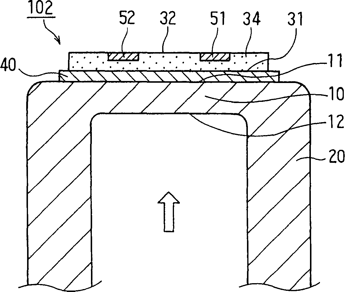
Wie
in den 3A und 3B gezeigt,
beinhaltet die Vorrichtung 102 eine Metallstütze 20 (Ständer), einen
intelligenten Halbleiterchip 34 und eine Glasschicht 40.
Die Metallstütze 20 umfasst
eine scheibenförmige
Membran 10. Der Chip 34 ist auf die Membran 10 unter
Verwendung der Glasschicht 40 aufgebondet. Der Chip 34 ist
in Kontakt mit der Glasschicht 40 an einer ersten Oberfläche 31 des
Chips 34. Die Membran 10 ist in Kontakt mit der
Glasschicht 40 an einer ersten Oberfläche 11 der Membran 10. Der
Chip 34 beinhaltet weiterhin vier rechteckförmige Messpunkte
(Erkennungselemente) 51, 52, 53, 54 oder
vier Piezo-Widerstände 51, 52, 53, 54,
sowie Verarbeitungsschaltkreiselemente.As in the 3A and 3B shown, includes the device 102 a metal support 20 (Stand), a smart semiconductor chip 34 and a glass layer 40 , The metal support 20 includes a disk-shaped membrane 10 , The chip 34 is on the membrane 10 using the glass layer 40 bonded on. The chip 34 is in contact with the glass layer 40 on a first surface 31 of the chip 34 , The membrane 10 is in contact with the glass layer 40 on a first surface 11 the membrane 10 , The chip 34 also contains four rectangular measuring points (recognition elements) 51 . 52 . 53 . 54 or four piezo resistors 51 . 52 . 53 . 54 , as well as processing circuit elements.
Obgleich
in der Figur nicht dargestellt, sind die Messpunkte 51 bis 54 durch
Verdrahtungslinien elektrisch miteinander verbunden, um einen Brückenschaltkreis
zu bilden. Die Verarbeitungsschaltkreiselemente werden verwendet,
einen Schaltkreis zu bilden, um eine elektrische Größe, beispielsweise Strom
und Potential zu verarbeiten, welche vom Brückenschaltkreis ausgegeben
wird. Wie in den 3A und 3B gezeigt,
sind die Messpunkte 51 bis 54 in einer zweiten
Oberfläche 32 des
Chips 34 gegenüberliegend
der ersten Oberfläche 31 oberhalb
der Membran 10 angeordnet. Die Verarbeitungsschaltkreiselemente
sind in einem Verarbeitungsschaltkreisbereich 71 enthalten,
der in der zweiten Oberfläche 32 des
Chips 34 liegt.Although not shown in the figure, the measurement points are 51 to 54 electrically interconnected by wiring lines to form a bridge circuit. The processing circuitry elements are used to form a circuit to process an electrical quantity, such as current and potential, that is output from the bridge circuit. As in the 3A and 3B shown are the measuring points 51 to 54 in a second surface 32 of the chip 34 opposite the first surface 31 above the membrane 10 arranged. The processing circuit elements are in a processing circuit area 71 included in the second surface 32 of the chip 34 lies.
Wenn
ein Medium wie ein Gas oder eine Flüssigkeit, welches beispielsweise
den Kraftstoffeinspritzdruck eines Motors überträgt, in die Stütze 20 eingebracht
wird, um den Druck auf eine zweite Oberfläche 12 der Membran 10 gegenüberliegend der
ersten Oberfläche 11 aufzubringen,
verformt sich die Membran 10 und der Chip 34 verformt
sich synchron, so dass die Widerstände an den Messpunkten 51 bis 54 geändert werden.
Die Widerstandsänderung ändert die
elektrische Größe, welche
vom Brückenschaltkreis
ausgegeben wird und die elektrische Größe wird von dem Schaltkreis
verarbeitet, der in dem Verarbeitungsschaltkreisbereich 71 enthalten ist,
um den Druck zu erfassen.When a medium such as a gas or a liquid, which transmits, for example, the fuel injection pressure of an engine, into the support 20 is introduced to the pressure on a second surface 12 the membrane 10 opposite the first surface 11 to apply, the membrane deforms 10 and the chip 34 deforms synchronously so that the resistors at the measuring points 51 to 54 be changed. The change in resistance changes the electrical quantity output by the bridge circuit and the electrical quantity is processed by the circuitry in the processing circuitry area 71 is included to capture the pressure.
Die
metallische Stütze 20 hat
die Form eines Hohlzylinders und wird beispielsweise durch spanabhebende
Bearbeitung gefertigt. Die Metallstütze 20 ist beispielsweise
aus KOVAR, was eine Fe-Ni-Co-Legierung ist, mit einem thermischen
Ausdehnungskoeffizienten annähernd
gleich demjenigen von Glas. Die Membran 10 ist an einem
ersten Ende der Metallstütze 20 angeordnet.
Das Medium, welches den Druck überträgt, wird
von einem zweiten Ende der Metallstütze 20 hier eingebracht,
welches in der Figur nicht darge stellt ist, jedoch gegenüber dem ersten
Ende liegt, wobei die Einbringung des Mediums in Richtung eines
Pfeils in 3B erfolgt, um Druck auf die
zweite Oberfläche 12 der
Membran 10 aufzubringen. Die Abmessungen der Metallstütze 20 sind
beispielsweise 6,5 mm Aussendurchmesser und 2,5 mm Innendurchmesser.
Die Dicke der Membran 10 beträgt 0,65 mm, wenn der maximal
erfassbare Druck beispielsweise 20 MPa beträgt und 1,40 mm, wenn der maximal
erfassbare Druck beispielsweise 200 MPa beträgt.The metallic prop 20 has the shape of a hollow cylinder and is made for example by machining. The metal support 20 is for example made of KOVAR, which is an Fe-Ni-Co alloy, with a thermal expansion coefficient approximately equal to that of glass. The membrane 10 is at a first end of the metal support 20 arranged. The medium which transfers the pressure is from a second end of the metal support 20 introduced here, which is not illustrated in the figure, however, is opposite the first end, wherein the introduction of the medium in the direction of an arrow in 3B takes place to pressure on the second surface 12 the membrane 10 applied. The dimensions of the metal support 20 are for example 6.5 mm outside diameter and 2.5 mm inside diameter. The thickness of the membrane 10 is 0.65 mm when the maximum detectable pressure is, for example, 20 MPa and 1.40 mm when the maximum detectable pressure is 200 MPa, for example.
Gemäß 4 beinhaltet
der Halbleiterchip 34 ein plattenförmiges Siliziumeinkristallsubstrat 80 des
p-Typs mit gleichförmiger
Dicke. Die Oberfläche des
Siliziumsubstrates 80, welche auf Seiten der zweiten Oberfläche 32 des
Chips 34 liegt, ist eben und hat eine Oberflächenausrichtung
von (100). Die Abmessungen des Halbleiterchips 34 betragen
beispielsweise 4,0 mm × 4,0
mm betreffend Länge
und Breite der ebenen Oberfläche
und 0,2 mm betreffend die Dicke. Die Glasschicht 40 ist
beispielsweise aus einem Glas mit niedrigem Schmelzpunkt gemacht. Die
Dicke der Glasschicht 40 beträgt beispielsweise 0,06 mm.According to 4 includes the semiconductor chip 34 a plate-shaped silicon single crystal substrate 80 p-type of uniform thickness. The surface of the silicon substrate 80 which are on the side of the second surface 32 of the chip 34 lies, is level and has a surface orientation of ( 100 ). The dimensions of the semiconductor chip 34 For example, 4.0 mm × 4.0 mm in terms of length and width of the flat surface and 0.2 mm in thickness. The glass layer 40 is made of, for example, a low melting point glass. The thickness of the glass layer 40 is for example 0.06 mm.
Die
Oberfläche
des Siliziumsubstrates 80 hat eine Flächenausrichtung von (100),
so dass das Substrat 80 zwei Kristallachsen von <110> hat, welche senkrecht
zueinander und parallel zur Oberfläche des Siliziumsubstrates 80 sind,
wie in 3A gezeigt. In 3A ist
eine der Kristallachsen <110> parallel zu der X-Achse,
wohingegen die andere Ausrichtungsachse <110> parallel zu der Y-Achse ist. Wie in 3A gezeigt,
sind die Messpunkte 51 bis 54 so angeordnet, dass
ihre Längsrichtungen
parallel zur X-Achse sind, wohingegen ihre Seitenrichtungen parallel
zur Y-Achse sind.The surface of the silicon substrate 80 has a surface orientation of ( 100 ), leaving the substrate 80 two crystal axes of < 110 > has, which are perpendicular to each other and parallel to the surface of the silicon substrate 80 are, as in 3A shown. In 3A is one of the crystal axes < 110 > parallel to the X axis, whereas the other alignment axis < 110 > is parallel to the Y axis. As in 3A shown are the measuring points 51 to 54 arranged so that their longitudinal directions are parallel to the X-axis, whereas their lateral directions are parallel to the Y-axis.
Die
Verarbeitungsschaltkreiselemente, welche in dem Verarbeitungsschaltkreisbereich 71 in
der zweiten Oberfläche 32 des
Halbleiterchips 34 angeordnet sind, sind solche, welche
einen bipolaren Transistor und einen Trimmwiderstand verwenden. Obgleich
in der Figur nicht gezeigt, sind die Verarbeitungsschaltkreiselemente
elektrisch mit den Messpunkten 51 bis 54 über Verdrahtungsleitungen
verbunden.The processing circuitry elements included in the processing circuitry area 71 in the second surface 32 of the semiconductor chip 34 are those which use a bipolar transistor and a trim resistor. Although not shown in the figure, the processing circuit elements are electrical with the measurement points 51 to 54 connected via wiring lines.
Nachfolgend
wird der Querschnittsaufbau des Halbleiterchips 34 genauer
beschrieben. Wie in 4 gezeigt, ist eine Mehrzahl
von n– Epitaxial bereichen 82a, 82b, 82c, 82d und 82e,
welche voneinander durch p+ Isolationsbereiche 81 isoliert
sind, in der Oberfläche
des Halbleitersubstrates 80 angeordnet. Die Messpunkte 51 bis 54 sind
in der Oberfläche von
einem (82) der Bereiche der Epitaxialregionen angeordnet.The cross-sectional structure of the semiconductor chip will be described below 34 described in more detail. As in 4 shown is a plurality of n - epitaxial regions 82a . 82b . 82c . 82d and 82e which are separated from each other by p + isolation regions 81 are isolated, in the surface of the semiconductor substrate 80 arranged. The measuring points 51 to 54 are in the surface of one ( 82 ) of the regions of the epitaxial regions.
Gemäß 4 sind
zwei Transistoren Tr1 und Tr2 zur Bildung eines Operationsverstärkers unter
Verwendung zweier Epitaxialbereiche 82b bzw. 82c ausgebildet.
Ein Trimmwiderstand 83, der zur Einstellung der Eigenschaften
des Operationsverstärkers
verwendet wird, ist in einem Epitaxialbereich 82d angeordnet.
Der Trimmwiderstand 83 wird beispielsweise aus Chromsilizium
(CrSi) gefertigt. Ein Elektrodenkissen 84, welches zur
elektrischen Verbindung des Halbleiterchips 30 mit einem
externen Schaltkreis verwendet wird, ist in einem Epitaxialbereich 82e angeordnet.
Das Elektrodenkissen 84 ist beispielsweise aus Aluminium
gefertigt. Die Transistoren Tr1, Tr2, der Trimmwiderstand 83 und
das Elektrodenkissen 84 sind in dem Verarbeitungsschaltkreisbereich 71 enthalten.According to 4 are two transistors Tr1 and Tr2 for forming an operational amplifier using two epitaxial regions 82b respectively. 82c educated. A trim resistor 83 which is used to adjust the characteristics of the operational amplifier is in an epitaxial region 82d arranged. The trim resistance 83 is made of chromium silicon (CrSi), for example. An electrode pad 84 , which is used for electrical connection of the semiconductor chip 30 used with an external circuit is in an epitaxial region 82e arranged. The electrode pad 84 is made of aluminum, for example. The transistors Tr1, Tr2, the trim resistor 83 and the electrode pad 84 are in the processing circuit area 71 contain.
Obgleich
in der Figur nicht dargestellt, sind andere Epitaxialbereiche in
der Oberfläche
des Halbleitersubstrates 80 angeordnet und ebenfalls voneinander
durch andere p+ Isolationsbereiche 81 elektrisch
isoliert. Weitere Widerstände
und Transistoren sind in den anderen Epitaxialbereichen angeordnet.Although not shown in the figure, other epitaxial regions are in the surface of the semiconductor substrate 80 arranged and also separated from each other by other p + isolation regions 81 electrically isolated. Further resistors and transistors are arranged in the other epitaxial regions.
Ein
Siliziumoxidfilm 86 (SiO2) ist
auf der Oberfläche
des Halbleitersubstrates 80 angeordnet. Verdrahtungslinien 85,
welche die Messpunkte 51 bis 54, die Transistoren
Tr1 und Tr2 den Trimmwiderstand 83 und das Elektrodenkissen 84 elektrisch
untereinander verbinden, sind von dem Halbleitersubstrat 80 an
bestimmten Abschnitten durch den Siliziumoxidfilm 86 isoliert.
Ein Passivierungsfilm 87, der als Schutzfilm dient, ist
auf den Verdrahtungsleitungen 85 und dem Siliziumoxidfilm 86 angeordnet.
Der Passivierungsfilm 87 hat eine Öffnung 87a für eine Drahtbondierung,
wie in 2 gezeigt. Der Passivierungsfilm 87 ist
beispielsweise aus einem Plasma-Silizium-Nitrid-Film (P-SiN) gefertigt.A silicon oxide film 86 (SiO 2 ) is on the surface of the semiconductor substrate 80 arranged. wiring lines 85 which are the measuring points 51 to 54 , the transistors Tr1 and Tr2 the trim resistor 83 and the electrode pad 84 electrically interconnect, are of the semiconductor substrate 80 at certain sections through the silicon oxide film 86 isolated. A passivation film 87 acting as a protective film is on the wiring lines 85 and the silicon oxide film 86 arranged. The passivation film 87 has an opening 87a for a wire bond, as in 2 shown. The passivation film 87 is made, for example, from a plasma silicon nitride film (P-SiN).
Nachfolgend
wird ein Verfahren zur Herstellung der Druckerkennungsvorrichtung 102 der 3A und 3B kurz
beschrieben. Die Druckerken nungsvorrichtung 102 der 3A und 3B wird
gemäß dem Prozessablauf
von 5 hergestellt. Zunächst werden als Vorbereitungsschritt
ein Halbleiterchip 34 mit den Messpunkten 51, 52, 53 und 54 und
den Verarbeitungsschaltkreiselementen, beispielsweise Transistoren
Tr1, Tr2 und einem Trimmwiderstand 83 und eine Metallstütze oder
ein Metallträger 20 vorbereitet.
Nachfolgend wird als Anbringschritt eine Glasschicht 40 aus
beispielsweise einem Glas mit niedrigem Schmelzpunkt an einer bestimmten
Position einer ersten Oberfläche 11 der Membran 10 der
Metallstütze 20 aufgebracht
und der Halbleiterchip 34 wird auf der Oberseite der Glasschicht 40 angeordnet.The following is a method for manufacturing development of the pressure detection device 102 of the 3A and 3B briefly described. The printer recognition device 102 of the 3A and 3B is according to the process flow of 5 produced. First, as a preparation step, a semiconductor chip 34 with the measuring points 51 . 52 . 53 and 54 and the processing circuit elements, for example, transistors Tr1, Tr2 and a trim resistor 83 and a metal support or a metal support 20 prepared. Hereinafter, as a mounting step, a glass layer 40 from, for example, a low melting point glass at a particular position of a first surface 11 the membrane 10 the metal support 20 applied and the semiconductor chip 34 is on top of the glass layer 40 arranged.
Dann
wird als Bondierungsschritt die kombinierte Einheit aus den Elementen 20, 40 und 34 in
einen Sinterofen gebracht, der in der Zeichnung nicht dargestellt
ist und die Glasschicht 40 wird bei annähernd 400°C gesintert, um den HalbleiterChip 344 an der
Metallstütze 20 anzubonden.
Schließlich
wird in einem Temperschritt die gesinterte kombinierte Einheit aus
den Elementen 20, 40 und 34 in eine Temperkammer
oder einen Kühlofen 90 gemäß 6 auf einer
Heizplatte 91 angeordnet und beispielsweise bei 380°C über 30 Minuten
auf der Heizplatte 91 gesintert, während ein wasserstoffhaltiges
Gas zugeführt
wird. Durch die obigen Schritte wird die Druckerkennungsvorrichtung 102 der 3A und 3B gebildet.Then, as a bonding step, the combined unit of the elements 20 . 40 and 34 brought into a sintering furnace, which is not shown in the drawing and the glass layer 40 is sintered at approximately 400 ° C to the semiconductor chip 344 on the metal support 20 to bond. Finally, in an annealing step, the sintered combined unit becomes the elements 20 . 40 and 34 in an annealing chamber or a cooling furnace 90 according to 6 on a hot plate 91 arranged and for example at 380 ° C for 30 minutes on the hot plate 91 sintered while a hydrogen-containing gas is supplied. Through the above steps, the pressure detecting device becomes 102 of the 3A and 3B educated.
Nachfolgend
wird der Druckerkennungsmechanismus bei der Druckerkennungsvorrichtung 102 der 3A und 3B im
Detail beschrieben. Wenn ein Medium, welches den zu erfassenden
Druck überträgt, in den
Träger 20 eingebracht
wird, um diesen Druck auf die zweite Oberfläche 12 der Membran 10 wirken
zu lassen, verformt sich die Membran 10 und der Halbleiterchip 34 verformt
sich synchron hiermit. Im Erebnis wird eine Belastung in dem Halbleiterchip 34 erzeugt.
Hierbei werden Spannungen oder Belastungen entlang der X-Achse und
der Y-Achse in 3A, welche jeweils parallel
zu zwei <110> Kristallachsen des
Halbleiterchips 34 sind, in jedem der Messpunkte 51, 52, 53 und 54 erzeugt.Hereinafter, the pressure detection mechanism in the pressure detection device 102 of the 3A and 3B described in detail. When a medium, which transfers the pressure to be detected, into the carrier 20 is introduced to this pressure on the second surface 12 the membrane 10 to let act, the membrane deforms 10 and the semiconductor chip 34 deforms synchronously herewith. The result is a load in the semiconductor chip 34 generated. Here are voltages or loads along the X-axis and the Y-axis in 3A , which are parallel to two < 110 > Crystal axes of the semiconductor chip 34 are, in each of the measuring points 51 . 52 . 53 and 54 generated.
Wenn
ein Druck auf die zweite Oberfläche 12 der
Membran 10 aufgebracht wird, haben die im Halbleiterchip 34 an
dem Abschnitt oberhalb der Membran 10 erzeugten Belastungen
oder Spannungen die Verteilungen ge mäß den 7A und 7B.
In 7A drücken
um welches in einer durchgezogenen Linie dargestellt ist und σyy,
welches gestrichelt dargestellt ist, die Größe der Belastung oder Spannung
entlang der X-Achse bzw. entlang der Y-Achse aus. Wie in 7A gezeigt,
nimmt σyy steiler ab, wenn der Abstand vom Mittelpunkt
K zunimmt, als dies σxx tut, obgleich sowohl σxx und σyy abnehmen,
wenn der Abstand vom Mittelpunkt K zunimmt.When a pressure on the second surface 12 the membrane 10 is applied, have in the semiconductor chip 34 at the section above the membrane 10 generated loads or voltages according to the distributions 7A and 7B , In 7A Pressing around which is shown in a solid line and σ yy , which is shown in dashed lines, the magnitude of the stress or stress along the X-axis or along the Y-axis. As in 7A σ yy decreases more steeply as the distance from the center K increases than does σ xx , although both σ xx and σ yy decrease as the distance from the center K increases.
Eine
elektrische Größe entsprechend
der Differenz D zwischen σxx und σyy kann von einem Brückenschaltkreis ausgegeben
werden, der aus den Messpunkten 51, 52, 53 und 54 gebildet
ist. Die elektrische Größe ist annähernd proportional
zu dem Unterschied D zwischen σxx und σyy. Somit kann der auf die zweite Oberfläche 12 der
Membran 10 aufgebrachte Druck präzise erfasst werden. Das Siliziumsubstrat 80 in
dem Halbleiterchip 34 hat eine Flächenausrichtung (100),
so dass zwei Kristallachsen von <110>, welche senkrecht
zueinander sind, und hohe Belastungsempfindlichkeit haben, auf der Oberfläche des
Siliziumsubstrates 80 liegen. Zusätzlich hat jeder der Messpunkte 51, 52, 53 und 54 zwei Arten
von Stress- oder Belastungspegeln, nämlich σxx und σyy.
Daher ist es möglich,
den Druck auf der Grundlage des oben genannten Erkennungsmechanismus
zu erkennen.An electrical quantity corresponding to the difference D between σ xx and σ yy can be output from a bridge circuit consisting of the measuring points 51 . 52 . 53 and 54 is formed. The electrical quantity is approximately proportional to the difference D between σ xx and σ yy . Thus, the on the second surface 12 the membrane 10 applied pressure can be detected precisely. The silicon substrate 80 in the semiconductor chip 34 has a surface orientation ( 100 ), so that two crystal axes of < 110 >, which are perpendicular to each other, and have high strain sensitivity, on the surface of the silicon substrate 80 lie. In addition, each of the measuring points has 51 . 52 . 53 and 54 two types of stress levels, namely σ xx and σ yy . Therefore, it is possible to detect the pressure based on the above-mentioned detection mechanism.
Wie
in 3A gezeigt, sind die Messpunkte 51, 52, 53 und 54 und
die Verarbeitungsschaltkreiselemente, welche in dem Verarbeitungsschaltkreisbereich 71 enthalten
sind, in dem Halbleiterchip 34 der Druckerkennungsvorrichtung 102 integriert.
Daher ist es möglich,
ein System, welches die intelligente Druckerkennungsvorrichtung 102 der 3A und 3B beinhaltet,
kleiner als ein System zu machen, welche die diskrete Druckerkennungsvorrichtung 100 gemäß den 1A und 1B beinhaltet.As in 3A shown are the measuring points 51 . 52 . 53 and 54 and the processing circuitry elements included in the processing circuitry area 71 are contained in the semiconductor chip 34 the pressure detection device 102 integrated. Therefore, it is possible to have a system using the intelligent pressure detection device 102 of the 3A and 3B involves making smaller than a system using the discrete pressure detection device 100 according to the 1A and 1B includes.
Beim
Herstellungsvorgang der Druckerkennungsvorrichtung 102 der 3A und 3B wird der
Halbleiterchip 34 getempert oder nachgeglüht, nachdem
die Glasschicht 40 gesintert worden ist. Wenn der Halbleiterchip 34 nicht
getempert werden würde,
würden
sich die Eigenschaften vom Transistor Tr1 oder Tr2, welche in dem
Verarbeitungsschaltkreis 71 als Verarbeitungsschaltkreiselemente
enthalten sind, sich aufgrund der folgenden Tatsachen ändern:
Wie
beschrieben, beinhaltet der Halbleiterchip 34 das Einkristall-Siliziumsubstrat 80 vom
p-Typ und die Aluminiumleitungen 85, der Siliziumoxidfilm 86 und der
Passivierungsfilm 87 sind auf der Oberfläche des Substrates
angeordnet. Der Siliziumoxidfilm 86 und der Passivierungsfilm 87 werden
bei dem Waferherstellungsvorgang in der Atmosphäre gebildet, welche Wasserstoff
enthält,
wobei bei dem Waferherstellungsvorgang ein Wafer bearbeitet wird,
um den Halbleiterchip 34 zu bilden. Wenn der Siliziumoxidfilm 86 und
der Passivierungsfilm 87 ausgebildet werden, wird der Wasserstoff
aus der Atmosphäre
in dem Siliziumoxidfilm 86 und dem Passivierungsfilm 87 in
Form von Wasserstoffionen absorbiert. Die freien Bindungen der Siliziumatome
an der Grenzfläche oder
Schnittstelle zwischen der Oberfläche des Substrates 80 und
des Siliziumoxidfilms 86 werden durch die Wasserstoffionen
begrenzt. In einem nachfolgenden Schritt des Waferherstellungsvorganges
wird der Wafer auf hohe Temperatur in der Atmosphäre erhitzt,
welche Wasserstoff enthält.
Während
dieses Schritts kann die Menge an Wasserstoffionen im Siliziumoxidfilm 86 und
im Passivierungsfilm 87 anwachsen, da Wasserstoff aus der
Atmosphäre
absorbiert wird und die Bindungen zwischen den durch Wasserstoff
eingegrenzten Siliziumatomen und den eingrenzenden Wasserstoffatomen
an der Schnittstelle zwischen der Oberfläche des Substrates 80 und
dem Siliziumoxidfilm 86 können aufgrund der hohen Temperatur
aufbrechen.In the manufacturing process of the pressure detecting device 102 of the 3A and 3B becomes the semiconductor chip 34 tempered or post-annealed after the glass layer 40 has been sintered. If the semiconductor chip 34 would not be annealed, the characteristics of the transistor Tr1 or Tr2, which are in the processing circuit 71 are included as processing circuit elements, change due to the following facts:
As described, the semiconductor chip includes 34 the single crystal silicon substrate 80 p-type and aluminum cables 85 , the silicon oxide film 86 and the passivation film 87 are arranged on the surface of the substrate. The silicon oxide film 86 and the passivation film 87 are formed in the wafer manufacturing process in the atmosphere containing hydrogen, and in the wafer manufacturing process, a wafer is processed to form the semiconductor chip 34 to build. When the silicon oxide film 86 and the passivation film 87 are formed, the hydrogen from the atmosphere in the silicon oxide film 86 and the passivation film 87 absorbed in the form of hydrogen ions. The free bonds of the silicon atoms at the interface or interface between the surface of the substrate 80 and the silicon oxide film 86 are limited by the hydrogen ions. In a following the step of the wafer manufacturing process, the wafer is heated to high temperature in the atmosphere containing hydrogen. During this step, the amount of hydrogen ions in the silicon oxide film 86 and in the passivation film 87 increase as hydrogen is absorbed from the atmosphere and the bonds between the hydrogen-confined silicon atoms and the confining hydrogen atoms at the interface between the surface of the substrate 80 and the silicon oxide film 86 can break because of the high temperature.
Wenn
jedoch in einem späteren
Schritt die Glasschicht 40 gesintert wird, können sich
die an der Schnittstelle zwischen der Oberfläche des Substrates 80 und
des Siliziumoxidfilms 86 an den Siliziumatomen gebundenen
Wasserstoffatome von den Siliziumatomen wegbewegen und die im Siliziumoxidfilm 86 absorbierten
Wasserstoffionen können
in Richtung des Passivierungsfilmes 87 wandern oder in
die Atmosphäre
ausgasen.However, if in a later step the glass layer 40 Sintered, which can be at the interface between the surface of the substrate 80 and the silicon oxide film 86 Moving hydrogen atoms bound to the silicon atoms away from the silicon atoms and those in the silicon oxide film 86 absorbed hydrogen ions can in the direction of the passivation film 87 wander out or into the atmosphere.
Im
Ergebnis werden Elektronen, welche von den Wasserstoffatomen im
Siliziumoxidfilm 86 gehalten sind, über die Oberfläche der
Transistoren Tr1 und Tr2 freigegeben, welche in dem Verarbeitungsschaltkreis 71 enthalten
sind und der Transistorinjektions-Wirkungsgrad der Transisistoren
Tr1 und Tr2 würde
anwachsen. Infolgedessen geht der Basisstrom hoch und der Kollektorstrom
geht auch zusammen mit den Strömen
hoch, welche durch die Basis, den Emitter und den Kollektor in jedem
der Transistoren Tr1 und Tr2 fließen. Somit wird der Stromverstärkungsfaktor,
der eine der Eigenschaften der Transistoren Tr1 und Tr2 ist, ansteigen.As a result, electrons are generated by the hydrogen atoms in the silicon oxide film 86 are released across the surface of the transistors Tr1 and Tr2 which are in the processing circuit 71 are included and the transistor injection efficiency of the transistors Tr1 and Tr2 would increase. As a result, the base current goes high and the collector current also goes up together with the currents flowing through the base, the emitter and the collector in each of the transistors Tr1 and Tr2. Thus, the current amplification factor, which is one of the characteristics of the transistors Tr1 and Tr2, will increase.
Aufgrund
der erwähnten
Eigenschaftsänderung
der Transistoren Tr1 und Tr2 haben die Transistoren Tr1 und Tr2
voneinander unterschiedliche Eigenschaften, wenn diese Transistoren
Tr1 und Tr2 relativ weit voneinander beabstandet sind. Im Ergebnis
verliert sich die Parität
des Operationsverstärkers,
der durch die Transistoren Tr1 und Tr2 gebildet ist und die Eigenschaften
des Operationsverstärkers verschlechtern
sich.by virtue of
the mentioned
property change
of the transistors Tr1 and Tr2 have the transistors Tr1 and Tr2
different properties when these transistors
Tr1 and Tr2 are relatively widely spaced. In the result
loses the parity
the operational amplifier,
which is formed by the transistors Tr1 and Tr2 and the characteristics
deteriorate the operational amplifier
yourself.
Zur
Lösung
dieses Problems wird, wie in den 5 und 6 gezeigt,
nachdem die Glasschicht 14 gesintert worden ist, der Halbleiterchip 34 durch Erhitzen
auf der Heizplatte 91 getempert, während ein wasserstoffhaltiges
Gas in die Temperkammer 90 beim Herstellungsprozess der
Druckerkennungsvorrichtung 102 der 3A und 3B eingebracht wird.
Selbst wenn sich somit die Wasserstoffatome, welche an der Schnittstelle
zwischen der Oberfläche des
Substrates 18 und des Siliziumoxidfilms 86 an den
Siliziumatomen gebunden sind, sich von den Siliziumatomen wegbewegen
und die Wasserstoffionen, welche im Siliziumoxidfilm 86 absorbiert
sind, in Richtung des Passivierungsfilms 87 wandern oder zur
Atmosphäre
hin ausgasen, ist es möglich,
Wasserstoffionen während
des Temperschrittes in den Siliziumoxidfilm 86 einzubringen.To solve this problem, as in the 5 and 6 shown after the glass layer 14 has been sintered, the semiconductor chip 34 by heating on the hot plate 91 annealed, while a hydrogen-containing gas in the annealing chamber 90 in the manufacturing process of the pressure detection device 102 of the 3A and 3B is introduced. Even if, therefore, the hydrogen atoms, which at the interface between the surface of the substrate 18 and the silicon oxide film 86 bonded to the silicon atoms, move away from the silicon atoms and the hydrogen ions, which in the silicon oxide film 86 absorbed in the direction of the passivation film 87 it is possible to outgas or vent to the atmosphere, it is possible to introduce hydrogen ions into the silicon oxide film during the annealing step 86 contribute.
Im
Ergebnis ist es möglich,
die Verringerung der Menge der Wasserstoffionen im Siliziumoxidfilm 86 zu
unterdrücken.
Somit ist es wiederum möglich, Änderungen
in dem Transistorinjektions-Wirkungsgrad der Transistoren Tr1 und
Tr2 zu unterdrücken. Im
Ergebnis ist es möglich, Änderungen
der Basisströme
in den Transistoren Tr1 und Tr2 zu unterdrücken. Weiterhin ist es möglich, Änderungen
im Stromverstärkungsfaktor
der Transistoren Tr1 und Tr2 zu unterdrücken.As a result, it is possible to reduce the amount of hydrogen ions in the silicon oxide film 86 to suppress. Thus, it is again possible to suppress changes in the transistor injection efficiency of the transistors Tr1 and Tr2. As a result, it is possible to suppress changes in the base currents in the transistors Tr1 and Tr2. Furthermore, it is possible to suppress changes in the current amplification factor of the transistors Tr1 and Tr2.
Wenn
ein Medium, welches den zu erfassenden Druck überträgt, den Druck auf die Membran 10 aufbringt,
verformt sich die Membran 10 und somit verformt sich auch
der Halbleiterchip 34 auf synchrone Weise. Hierbei verformt
sich jedoch auch der Verarbeitungsschaltkreisbereich 71 und
im Verarbeitungsschaltkreisbereich 71 wird eine Belastung
erzeugt. Aufgrund dieser Belastung können elektrische Felder in
den Transistoren Tr1 und Tr2, welche in dem Verarbeitungsschaltkreis 71 angeordnet
sind, sich lokal konzentrieren und ein "hot carrier"-Phänomen
kann verursacht werden. Dies bedeutet, dass Ladungsträger, die
in den konzentrierten elektrischen Feldern beschleunigt werden,
in den Siliziumoxidfilm 86 oberhalb der Transistoren Tr1
und Tr2 eintreten. Hier können
die Ladungsträger
eingefangen werden, so dass die Schwellenwertspannungen der Transistoren
Tr1 und Tr2 geändert
werden.When a medium which transfers the pressure to be detected, the pressure on the membrane 10 applies, deforms the membrane 10 and thus also deforms the semiconductor chip 34 in a synchronous way. At the same time, however, the processing circuit area is also deformed 71 and in the processing circuitry area 71 a load is generated. Due to this loading, electric fields can be generated in the transistors Tr1 and Tr2 which are in the processing circuit 71 are located, concentrate locally and a "hot carrier" phenomenon can be caused. This means that carriers that are accelerated in the concentrated electric fields, in the silicon oxide film 86 enter above the transistors Tr1 and Tr2. Here, the carriers can be captured so that the threshold voltages of the transistors Tr1 and Tr2 are changed.
Zur
Beseitigung des Problems aufgrund des "hot carrier"-Phänomens
wird gemäß 3A der Verarbeitungsschaltkreisbereich 71 am
Umfang des Halbleiterchips 34 angeordnet. Genauer gesagt,
der Verarbeitungsschaltkreisbereich 71 liegt ausserhalb des
Abschnittes des Halbleiterchips 34, der oberhalb der Membran 10 der
Metallstütze 20 liegt.
Die im Halbleiterchip 34 erzeugten Belastungen oder Spannungen
sind an dem Verarbeitungsschaltkreisbereich 71 erheblich
geringer als an den Messpunkten 51, 52, 53 und 54.
Im Ergebnis ist es möglich,
das "hot carrier"-Phänomen zu
unterdrücken,
welches ansonsten in dem Verarbeitungsschaltkreisbereich 71 erzeugt
werden würde.
Somit ist es möglich,
Eigenschaftsänderungen
der Elemente, beispielsweise der Transistoren Tr1, Tr2 in dem Verarbeitungsschaltkreisbereich 71 noch
weiter zu unterdrücken.
Gemäß 7A ist
es bevorzugt, dass der Verarbeitungsschaltkreisbereich 71 mehr
als 2 mm entfernt vom Mittelpunkt K ist, so dass der Verarbeitungsschaltkreisbereich 71 eine
Belastung nicht größer als
0,01 kgf/mm2 erfährt.To eliminate the problem due to the "hot carrier" phenomenon is described in 3A the processing circuit area 71 on the periphery of the semiconductor chip 34 arranged. More specifically, the processing circuit area 71 is outside the section of the semiconductor chip 34 , above the membrane 10 the metal support 20 lies. The in the semiconductor chip 34 generated stresses or strains are at the processing circuitry area 71 considerably lower than at the measuring points 51 . 52 . 53 and 54 , As a result, it is possible to suppress the "hot carrier" phenomenon which otherwise occurs in the processing circuitry area 71 would be generated. Thus, it is possible to change property of the elements such as the transistors Tr1, Tr2 in the processing circuit area 71 even further to suppress. According to 7A it is preferable that the processing circuit area 71 is more than 2 mm away from the center K, so that the processing circuit area 71 a load not greater than 0.01 kgf / mm 2 learns.
Zusätzlich ist
die in dem Siliziumsubstrat 80 erzeugte Belastung entlang
der beiden Kristallachsen von <110> welche parallel zur
Oberfläche
des Siliziumsubstrates 80 sind, das eine Oberflächenorientierung
von (100) hat, ganz erheblich. Von daher ist es bevorzugt,
dass der Verarbeitungsschaltkreisbereich so angeordnet wird, dass
die Seiten des Verarbeitungsschaltkreisbereiches einen Winkel von
45° bezüglich der
beiden Kristallachsen von <110> haben, wie dies bei
dem Verarbeitungsschaltkreisbereich 72 eines Halbleiterchips 35 in
einer Druckerkennungsvorrichtung 103 gemäß den 8A und 8B der
Fall ist. In den verbleibenden Aspekten ist die Druckerkennungsvorrichtung 103 der 8A und 8B im
Aufbau gleich der Druckerkennungsvorrichtung 102 der 3A und 3B.
Bei der genannten An ordnung des Verarbeitungsschaltkreisbereiches 72 erfährt der
Verarbeitungsschaltkreisbereich 72 entlang seiner Seiten
relativ geringe Belastungen. Von daher wird das "hot carrier-Phänomen" in dem Verarbeitungsschaltkreisbereich 72 weiter
unterdrückt.In addition, that is in the silicon substrate 80 generated stress along the two Kristallach sen of < 110 > which parallel to the surface of the silicon substrate 80 are that have a surface orientation of ( 100 ) has, quite considerably. Therefore, it is preferable that the processing circuit region be arranged so that the sides of the processing circuit region are at an angle of 45 ° with respect to the two crystal axes of < 110 > as with the processing circuitry area 72 a semiconductor chip 35 in a pressure detection device 103 according to the 8A and 8B the case is. In the remaining aspects, the pressure detection device 103 of the 8A and 8B similar in construction to the pressure detection device 102 of the 3A and 3B , In the above-mentioned arrangement of the processing circuit area 72 learns the processing circuitry area 72 along its sides relatively low loads. Therefore, the "hot carrier phenomenon" becomes in the processing circuit area 72 further suppressed.
Gemäß den 9A und 9B ist
eine Erkennungsvorrichtung für
eine dynamische Größe gemäß einer
nicht zum Gegenstand der vorliegenden Erfindung gehörenden Ausführungsform
eine intelligente Druckerkennungsvorrichtung 104, welche ähnlichen
Aufbau wie die erfindungsgemäße Druckerkennungsvorrichtung 102 der 3A und 3B hat.
Obgleich in der Figur nicht dargestellt, hat ein Halbleiterchip 36 in
den 9A und 9B ähnlichen
Querschnittsaufbau zu dem Halbleiterchip 34 der 3A und 3B,
der in 4 gezeigt ist. Die Druckerkennungsvorrichtung 104 der 9A und 9B unterscheidet
sich jedoch im Herstellungsverfahren von der Druckerkennungsvorrichtung 102 der 3A und 3B,
wie in dem Herstellungsablauf von 10 gezeigt.
Die Druckerkennungsvorrichtung 104 der 9A und 9B wird
gemäß diesem
Ablauf von 10 hergestellt.According to the 9A and 9B For example, a dynamic size recognizer according to an embodiment not belonging to the subject invention is an intelligent print recognizer 104 , which has a similar construction to the pressure-detecting device according to the invention 102 of the 3A and 3B Has. Although not shown in the figure, has a semiconductor chip 36 in the 9A and 9B similar cross-sectional structure to the semiconductor chip 34 of the 3A and 3B who in 4 is shown. The pressure detection device 104 of the 9A and 9B However, it differs in the manufacturing process of the pressure detection device 102 of the 3A and 3B as in the production process of 10 shown. The pressure detection device 104 of the 9A and 9B is according to this expiration of 10 produced.
Zunächst wird
in einem Vorbereitungsschritt ein Halbleiterchip 36, der
Messpunkte (Erkennungselemente) 51, 52, 53 und 54 und
Verarbeitungsschaltkreiselemente, beispielsweise Transistoren Tr1,
Tr2 und einen Trimmwiderstand 83 aufweist, sowie eine Metallstütze oder
einen Träger 20 vorbereitet.
In einem Anordnungsschritt wird eine Glasschicht 40, welche
beispielsweise aus Glas mit niedrigem Schmelzpunkt gebildet ist,
auf einen bestimmten Bereich auf der ersten Oberfläche 11 der
Membran 10 der Metallstütze 20 angebracht
und der Halbleiterchip 36 wird auf die Oberseite der Glasschicht 40 aufgesetzt.
Dann wird in einem Bondierungsschritt die kombinierte Einheit der
Elemente 20, 40 und 36 in einen Sinterofen
gebracht, der in der Zeichnung nicht dargestellt ist, und die Glasschicht 40 wird
bei annähernd
400°C gesintert,
um den Halbleiterchip 36 an die Metallstütze 20 anzubonden.First, in a preparation step, a semiconductor chip 36 , the measuring points (recognition elements) 51 . 52 . 53 and 54 and processing circuit elements such as transistors Tr1, Tr2 and a trim resistor 83 has, as well as a metal support or a carrier 20 prepared. In an arranging step, a glass layer is formed 40 formed of, for example, low melting point glass, to a certain area on the first surface 11 the membrane 10 the metal support 20 attached and the semiconductor chip 36 gets on top of the glass layer 40 placed. Then, in a bonding step, the combined unit of elements becomes 20 . 40 and 36 placed in a sintering furnace, which is not shown in the drawing, and the glass layer 40 is sintered at approximately 400 ° C to the semiconductor chip 36 to the metal support 20 to bond.
Die
obigen Schritte sind ähnlich
wie diejenigen bei der Druckerkennungsvorrichtung 102 der 3A und 3B.
Bei dem Herstellungsvorgang der Druckerkennungsvorrichtung 104 der 9A und 9B wird
jedoch in einem Trimmschritt der Trimmwiderstand 83 getrimmt,
um den Widerstand hiervon einzustellen, was unter Verwendung eines bekannten
Trimmverfahrens erfolgt, um Eigenschaftsänderungen der Transistoren
Tr1 und Tr2 zu kompensieren, welche während des Bondierungsschrittes
verursacht wurden. Mit den obigen Verfahrensschritten wird die Druckerkennungsvorrichtung 104 der 9A und 9B gebildet.The above steps are similar to those in the pressure detection device 102 of the 3A and 3B , In the manufacturing process of the pressure detection device 104 of the 9A and 9B However, in a trim step the trim resistance 83 trimmed to adjust the resistance thereof, which is done using a known trimming method to compensate for property changes of the transistors Tr1 and Tr2 caused during the bonding step. With the above process steps, the pressure detecting device becomes 104 of the 9A and 9B educated.
Der
erläuterte
Herstellungsvorgang bei der Druckerkennungsvorrichtung 104 der 9A und 9B zeichnet
sich dadurch aus, dass der Trimmwiderstand 83 getrimmt
oder eingestellt wird, um seinen Widerstandswert einzustellen, so
dass Eigenschaftsänderungen
der Transistoren Tr1 und Tr2 nach dem Bondierungsschritt kompensiert
werden. Selbst wenn sich somit Wasserstoffatome, welche an den Siliziumatomen
an der Schnittstelle zwischen der Oberfläche des Substrates 80 und
dem Siliziumoxidfilm 86 gebunden waren, von den Siliziumatomen wegbewegen
und Wasserstoffionen, welche in dem Siliziumoxidfilm 86 absorbiert
waren, in Richtung des Passivierungsfilms 87 wandern oder
in die Atmosphäre
ausgasen, und sich somit die elektrischen Eigenschaften der Transistoren
Tr1 und Tr2 nach dem Bondierunsschritt ändern, ist es möglich, dass
der Operationsverstärker,
der aus den Transistoren Tr1 und Tr2 gebildet ist, nach dem Trimmschritt
zufriedenstellend arbeitet.The explained manufacturing process in the pressure detection device 104 of the 9A and 9B is characterized by the fact that the trim resistance 83 is trimmed or adjusted to adjust its resistance so that property changes of the transistors Tr1 and Tr2 are compensated after the bonding step. Thus, even if there are hydrogen atoms attached to the silicon atoms at the interface between the surface of the substrate 80 and the silicon oxide film 86 were bound to move away from the silicon atoms and hydrogen ions contained in the silicon oxide film 86 absorbed in the direction of the passivation film 87 or outgrow the atmosphere and thus change the electrical characteristics of the transistors Tr1 and Tr2 after the bonding step, it is possible that the operational amplifier formed of the transistors Tr1 and Tr2 operates satisfactorily after the trimming step.
Der
Umfang der vorliegenden Erfindung ist nicht auf die oben genannte
Druckerkennungsvorrichtung beschränkt und kann auf verschiedene
andere Erkennungsvorrichtungen für
dynamische Größen, beispielsweise
bei Beschleunigungssensoren angewendet werden. Zusätzlich können die
Herstellungsverfahren und die Anordnung der Messpunkte 51 bis 54 und
des Verarbeitungsschaltkreisbereiches 71, 72 oder 73 auf
verschiedene Arten abgewandelt werden.The scope of the present invention is not limited to the above-mentioned pressure detecting device and can be applied to various other dynamic quantity detecting devices such as acceleration sensors. In addition, the manufacturing process and the arrangement of the measuring points 51 to 54 and the processing circuit area 71 . 72 or 73 be modified in different ways.
Wenn
beispielsweise der Verarbeitungsschaltkreisbereich 72 von 8A so
angeordnet wird, dass seine Seiten einen Winkel von 45° bezüglich der
beiden Kristallachsen von <110> einnehmen, wie in 8A gezeigt,
können
die Photomaskenmuster für
den Verarbeitungsschaltkreisbereich 72 von 8A durch Ändern der
Daten für
die Photomaskenmuster für
den Verarbeitungsschaltkreisbereich 71 von 3A gefertigt
werden, um die Musterungen um ungefähr 45° zu verdrehen.For example, if the processing circuitry area 72 from 8A is arranged so that its sides are at an angle of 45 ° with respect to the two crystal axes of < 110 > ingest, as in 8A The photomask patterns for the processing circuitry area may be shown 72 from 8A by changing the data for the photomask patterns for the processing circuit area 71 from 3A be made to twist the patterns by about 45 °.
Weiterhin
ist es beispielsweise möglich,
einen Siliziumwafer zu verwenden, der eine Oberflächenausrichtung
von (100) und eine Ausrichtungsfläche von 45° bezüglich der Kristallachsen von <110> hat. In diesem Fall
können
die Photomaskenmuster für
den Verarbeitungsschaltkreisbereich 72 von 8A lediglich
durch Verschieben der Photomaskenmuster des Verarbeitungsschaltkreisbereiches 71 von 3A gemacht
werden, ohne dass die Daten für
die Photomaskenmuster des Verarbeitungsschaltkreisbereiches 71 von 3A geändert werden,
um die Muster zu drehen. Hierdurch kann der Herstellungsvorgang
für die
Photomasken des Verarbeitungsschaltkreisbereiches 72 von 8A vereinfacht
werden.Furthermore, for example, it is possible to use a silicon wafer having a surface orientation of (FIG. 100 ) and an orientation surface of 45 ° with respect to the crystal axes of < 110 > Has. In this case, the photomask patterns for the processing circuit area 72 from 8A merely by shifting the photomask patterns of the processing circuit area 71 from 3A be made without the data for the photomask pattern of the processing circuit area 71 from 3A be changed to rotate the patterns. Thereby, the manufacturing process for the photomasks of the processing circuit area 72 from 8A be simplified.
Der
Verarbeitungsschaltkreisbereich 72 von 8A ist
so angeordnet, dass seine Seiten einen Winkel von 45° bezüglich der
Seiten des Halbleiterchips 35 haben, welche parallel zu
den Kristallachsen von <110> sind. Alternativ hierzu
können
in einer Druckerkennungsvorrichtung 105 gemäß den 11A und 11B die
Seiten eines Verarbeitungsschaltkreisbereiches 74 parallel
zu den Seiten des Halbleiterchips 37 sein, welche parallel
zu den Kristallachsen von <110> sind, wohingegen die
Messpunkte 51 bis 54 so angeordnet sind, dass
ihre Längsrichtungen
einen Winkel von 45 Grad bezüglich
der Seiten des Halbleiterchips 37 haben, mit anderen Worten,
die Längsrichtungen
von ihnen sind parallel zu den Kristallachsen von <110>. Ansonsten ist die
Druckerkennungsvorrichtung 105 der 11A und 11B vom gleichen Aufbau wie die Druckerkennungsvorrichtung 102 der 3A und 3B.The processing circuit area 72 from 8A is arranged so that its sides are at an angle of 45 ° with respect to the sides of the semiconductor chip 35 which are parallel to the crystal axes of < 110 > are. Alternatively, in a pressure detection device 105 according to the 11A and 11B the sides of a processing circuit area 74 parallel to the sides of the semiconductor chip 37 which are parallel to the crystal axes of < 110 > are, whereas the measuring points 51 to 54 are arranged so that their longitudinal directions at an angle of 45 degrees with respect to the sides of the semiconductor chip 37 in other words, the longitudinal directions of them are parallel to the crystal axes of < 110 >. Otherwise, the pressure detection device 105 of the 11A and 11B of the same structure as the pressure detection device 102 of the 3A and 3B ,
Der
Halbleiterchip 34 wird durch Erwärmen auf der Heizplatte 91 getempert,
während
ein wasserstoffhaltiges Gas in die Temperkammer oder den Kühlofen 90 gebracht
wird, um Wasserstoffionen dem Siliziumoxidfilm 86 zuzuführen, nachdem
der Bondierungsschritt in dem Herstellungsvorgang für die Druckerkennungsvorrichtung 102 von 3A und 3B abgeschlossen
ist. Es ist jedoch auch möglich,
Wasserstoffionen dem Siliziumoxidfilm 86 durch thermisches
Abscheiden von Wasserstoffkomponenten oder durch Abscheiden von
Wasserstoffkomponenten unter Verwendung eines Plasmas oder von Ultraviolettstrahlung
zuzuführen.The semiconductor chip 34 is by heating on the hot plate 91 annealed, while a hydrogen-containing gas in the annealing chamber or the cooling furnace 90 is brought to hydrogen ions the silicon oxide film 86 after the bonding step in the manufacturing process for the pressure detecting device 102 from 3A and 3B is completed. However, it is also possible for hydrogen ions to be the silicon oxide film 86 by thermally depositing hydrogen components or by depositing hydrogen components using a plasma or ultraviolet radiation.
Beschrieben
wurde ein Verfahren zur Herstellung einer Erkennungsvorrichtung
für eine
dynamische Größe, welche
gebildet ist durch Anbonden eines Halbleiterchips, der ein Erkennungselement aufweist
zur Erkennung der dynamischen Größe, an eine
Stütze
unter Verwendung einer Bondierungsschicht, wobei das Verfahren aufweist:
Ausbilden eines Halbleiterchips, der ein Erkennungselement zur Verwendung
bei der Korrelation einer dynamischen Größe, welche zu erkennen ist,
mit einer elektrischen Größe und eine
Mehrzahl von Verarbeitungsschaltkreiselementen zur Bildung eines
Schaltkreises, der die elektrische Größe verarbeitet, aufweist; Anbringen
einer Bondierungsschicht auf einer Stütze; Anbringen des Halbleiterchips
auf der Bondierungsschicht; Sondieren des Halbleiterchips an der
Stütze durch
Sintern der Bondierungsschicht und Tempern des Halbleiterchips in
einer Atmosphäre,
welche Wasserstoff enthält,
um eine Änderung
in einer Eigenschaft eines der Verarbeitungsschaltkreiselemente
zu heilen, wobei besagte Änderung
während des
Bondierens des Halbleiterchips verursacht wurde.described
has been a method of making a recognition device
for one
dynamic size, which
is formed by bonding a semiconductor chip having a recognition element
to detect the dynamic size, to a
support
using a bonding layer, the method comprising:
Forming a semiconductor chip having a recognition element for use
in the correlation of a dynamic variable, which can be recognized
with an electrical size and a
A plurality of processing circuit elements for forming a
Circuit that processes the electrical size has; install
a bonding layer on a support; Attaching the semiconductor chip
on the bonding layer; Probing the semiconductor chip at the
Stay through
Sintering the bonding layer and annealing the semiconductor chip in
an atmosphere,
which contains hydrogen,
a change
in a characteristic of one of the processing circuit elements
to heal, said change
during the
Bonding of the semiconductor chip was caused.