DE102012113168A1 - Photodiode arrays and manufacturing processes - Google Patents
Photodiode arrays and manufacturing processes Download PDFInfo
- Publication number
- DE102012113168A1 DE102012113168A1 DE102012113168A DE102012113168A DE102012113168A1 DE 102012113168 A1 DE102012113168 A1 DE 102012113168A1 DE 102012113168 A DE102012113168 A DE 102012113168A DE 102012113168 A DE102012113168 A DE 102012113168A DE 102012113168 A1 DE102012113168 A1 DE 102012113168A1
- Authority
- DE
- Germany
- Prior art keywords
- layer
- doped
- photodiode array
- silicon wafer
- epitaxial layer
- Prior art date
- Legal status (The legal status is an assumption and is not a legal conclusion. Google has not performed a legal analysis and makes no representation as to the accuracy of the status listed.)
- Withdrawn
Links
- 238000004519 manufacturing process Methods 0.000 title claims abstract description 30
- 238000003491 array Methods 0.000 title abstract description 6
- XUIMIQQOPSSXEZ-UHFFFAOYSA-N Silicon Chemical compound [Si] XUIMIQQOPSSXEZ-UHFFFAOYSA-N 0.000 claims abstract description 49
- 229910052710 silicon Inorganic materials 0.000 claims abstract description 45
- 239000010703 silicon Substances 0.000 claims abstract description 45
- 239000000758 substrate Substances 0.000 claims abstract description 31
- 238000000034 method Methods 0.000 claims description 62
- 230000008569 process Effects 0.000 claims description 43
- 239000004065 semiconductor Substances 0.000 claims description 11
- 229910004298 SiO 2 Inorganic materials 0.000 claims description 9
- 238000000151 deposition Methods 0.000 claims description 9
- 229910021420 polycrystalline silicon Inorganic materials 0.000 claims description 9
- 229910052751 metal Inorganic materials 0.000 claims description 8
- 239000002184 metal Substances 0.000 claims description 8
- 238000005530 etching Methods 0.000 claims description 7
- 230000000295 complement effect Effects 0.000 claims description 6
- VYPSYNLAJGMNEJ-UHFFFAOYSA-N Silicium dioxide Chemical compound O=[Si]=O VYPSYNLAJGMNEJ-UHFFFAOYSA-N 0.000 claims description 5
- 229910044991 metal oxide Inorganic materials 0.000 claims description 5
- 150000004706 metal oxides Chemical class 0.000 claims description 5
- 238000007781 pre-processing Methods 0.000 claims description 3
- 239000000377 silicon dioxide Substances 0.000 claims description 2
- 235000012239 silicon dioxide Nutrition 0.000 claims description 2
- 229920005591 polysilicon Polymers 0.000 claims 4
- 238000003384 imaging method Methods 0.000 description 33
- 238000002591 computed tomography Methods 0.000 description 12
- 239000000463 material Substances 0.000 description 11
- 238000012545 processing Methods 0.000 description 11
- 238000001465 metallisation Methods 0.000 description 7
- 238000003860 storage Methods 0.000 description 7
- 230000008021 deposition Effects 0.000 description 6
- 238000013170 computed tomography imaging Methods 0.000 description 5
- 238000010586 diagram Methods 0.000 description 5
- 238000009792 diffusion process Methods 0.000 description 5
- 230000006870 function Effects 0.000 description 5
- 230000004044 response Effects 0.000 description 5
- 238000000407 epitaxy Methods 0.000 description 4
- 238000002955 isolation Methods 0.000 description 4
- 238000000206 photolithography Methods 0.000 description 4
- 229910000679 solder Inorganic materials 0.000 description 4
- 238000012879 PET imaging Methods 0.000 description 3
- 238000004891 communication Methods 0.000 description 3
- 238000004590 computer program Methods 0.000 description 3
- 239000002019 doping agent Substances 0.000 description 3
- 238000005286 illumination Methods 0.000 description 3
- 230000007246 mechanism Effects 0.000 description 3
- 230000003287 optical effect Effects 0.000 description 3
- 238000002600 positron emission tomography Methods 0.000 description 3
- IJGRMHOSHXDMSA-UHFFFAOYSA-N Atomic nitrogen Chemical compound N#N IJGRMHOSHXDMSA-UHFFFAOYSA-N 0.000 description 2
- 239000004593 Epoxy Substances 0.000 description 2
- PXHVJJICTQNCMI-UHFFFAOYSA-N Nickel Chemical compound [Ni] PXHVJJICTQNCMI-UHFFFAOYSA-N 0.000 description 2
- OAICVXFJPJFONN-UHFFFAOYSA-N Phosphorus Chemical compound [P] OAICVXFJPJFONN-UHFFFAOYSA-N 0.000 description 2
- 229910052782 aluminium Inorganic materials 0.000 description 2
- XAGFODPZIPBFFR-UHFFFAOYSA-N aluminium Chemical compound [Al] XAGFODPZIPBFFR-UHFFFAOYSA-N 0.000 description 2
- 238000005229 chemical vapour deposition Methods 0.000 description 2
- 238000005468 ion implantation Methods 0.000 description 2
- 229910052698 phosphorus Inorganic materials 0.000 description 2
- 239000011574 phosphorus Substances 0.000 description 2
- 238000002603 single-photon emission computed tomography Methods 0.000 description 2
- ZOXJGFHDIHLPTG-UHFFFAOYSA-N Boron Chemical compound [B] ZOXJGFHDIHLPTG-UHFFFAOYSA-N 0.000 description 1
- OKTJSMMVPCPJKN-UHFFFAOYSA-N Carbon Chemical compound [C] OKTJSMMVPCPJKN-UHFFFAOYSA-N 0.000 description 1
- GYHNNYVSQQEPJS-UHFFFAOYSA-N Gallium Chemical compound [Ga] GYHNNYVSQQEPJS-UHFFFAOYSA-N 0.000 description 1
- JMASRVWKEDWRBT-UHFFFAOYSA-N Gallium nitride Chemical compound [Ga]#N JMASRVWKEDWRBT-UHFFFAOYSA-N 0.000 description 1
- 230000004913 activation Effects 0.000 description 1
- 239000000853 adhesive Substances 0.000 description 1
- 230000001070 adhesive effect Effects 0.000 description 1
- 229910052785 arsenic Inorganic materials 0.000 description 1
- RQNWIZPPADIBDY-UHFFFAOYSA-N arsenic atom Chemical compound [As] RQNWIZPPADIBDY-UHFFFAOYSA-N 0.000 description 1
- 230000005540 biological transmission Effects 0.000 description 1
- 229910052796 boron Inorganic materials 0.000 description 1
- 239000000919 ceramic Substances 0.000 description 1
- 239000011248 coating agent Substances 0.000 description 1
- 238000000576 coating method Methods 0.000 description 1
- 239000004020 conductor Substances 0.000 description 1
- 238000005137 deposition process Methods 0.000 description 1
- 238000013461 design Methods 0.000 description 1
- 238000011161 development Methods 0.000 description 1
- 230000005611 electricity Effects 0.000 description 1
- 230000007717 exclusion Effects 0.000 description 1
- 239000000945 filler Substances 0.000 description 1
- -1 for example Substances 0.000 description 1
- 229910052733 gallium Inorganic materials 0.000 description 1
- 229910002804 graphite Inorganic materials 0.000 description 1
- 239000010439 graphite Substances 0.000 description 1
- 239000007943 implant Substances 0.000 description 1
- 229910052738 indium Inorganic materials 0.000 description 1
- APFVFJFRJDLVQX-UHFFFAOYSA-N indium atom Chemical compound [In] APFVFJFRJDLVQX-UHFFFAOYSA-N 0.000 description 1
- 230000010354 integration Effects 0.000 description 1
- 150000002500 ions Chemical class 0.000 description 1
- 238000011068 loading method Methods 0.000 description 1
- 238000002595 magnetic resonance imaging Methods 0.000 description 1
- 238000009607 mammography Methods 0.000 description 1
- 238000005259 measurement Methods 0.000 description 1
- 229910052759 nickel Inorganic materials 0.000 description 1
- 229910052757 nitrogen Inorganic materials 0.000 description 1
- 238000009206 nuclear medicine Methods 0.000 description 1
- 230000003647 oxidation Effects 0.000 description 1
- 238000007254 oxidation reaction Methods 0.000 description 1
- 229920002120 photoresistant polymer Polymers 0.000 description 1
- 238000001020 plasma etching Methods 0.000 description 1
- 238000005498 polishing Methods 0.000 description 1
- 238000002360 preparation method Methods 0.000 description 1
- 229910052761 rare earth metal Inorganic materials 0.000 description 1
- 150000002910 rare earth metals Chemical class 0.000 description 1
- 238000009877 rendering Methods 0.000 description 1
- 238000005070 sampling Methods 0.000 description 1
- 238000000926 separation method Methods 0.000 description 1
- 229910052814 silicon oxide Inorganic materials 0.000 description 1
- 239000002210 silicon-based material Substances 0.000 description 1
- 239000011343 solid material Substances 0.000 description 1
- 238000003325 tomography Methods 0.000 description 1
- 238000012285 ultrasound imaging Methods 0.000 description 1
Images

Classifications
-
- H—ELECTRICITY
- H01—ELECTRIC ELEMENTS
- H01L—SEMICONDUCTOR DEVICES NOT COVERED BY CLASS H10
- H01L27/00—Devices consisting of a plurality of semiconductor or other solid-state components formed in or on a common substrate
- H01L27/14—Devices consisting of a plurality of semiconductor or other solid-state components formed in or on a common substrate including semiconductor components sensitive to infrared radiation, light, electromagnetic radiation of shorter wavelength or corpuscular radiation and specially adapted either for the conversion of the energy of such radiation into electrical energy or for the control of electrical energy by such radiation
- H01L27/144—Devices controlled by radiation
- H01L27/146—Imager structures
- H01L27/14683—Processes or apparatus peculiar to the manufacture or treatment of these devices or parts thereof
- H01L27/14698—Post-treatment for the devices, e.g. annealing, impurity-gettering, shor-circuit elimination, recrystallisation
-
- H—ELECTRICITY
- H01—ELECTRIC ELEMENTS
- H01L—SEMICONDUCTOR DEVICES NOT COVERED BY CLASS H10
- H01L27/00—Devices consisting of a plurality of semiconductor or other solid-state components formed in or on a common substrate
- H01L27/14—Devices consisting of a plurality of semiconductor or other solid-state components formed in or on a common substrate including semiconductor components sensitive to infrared radiation, light, electromagnetic radiation of shorter wavelength or corpuscular radiation and specially adapted either for the conversion of the energy of such radiation into electrical energy or for the control of electrical energy by such radiation
- H01L27/144—Devices controlled by radiation
- H01L27/146—Imager structures
- H01L27/14643—Photodiode arrays; MOS imagers
- H01L27/14658—X-ray, gamma-ray or corpuscular radiation imagers
- H01L27/14663—Indirect radiation imagers, e.g. using luminescent members
-
- H—ELECTRICITY
- H01—ELECTRIC ELEMENTS
- H01L—SEMICONDUCTOR DEVICES NOT COVERED BY CLASS H10
- H01L31/00—Semiconductor devices sensitive to infrared radiation, light, electromagnetic radiation of shorter wavelength or corpuscular radiation and specially adapted either for the conversion of the energy of such radiation into electrical energy or for the control of electrical energy by such radiation; Processes or apparatus specially adapted for the manufacture or treatment thereof or of parts thereof; Details thereof
- H01L31/02—Details
- H01L31/0224—Electrodes
- H01L31/022408—Electrodes for devices characterised by at least one potential jump barrier or surface barrier
-
- H—ELECTRICITY
- H01—ELECTRIC ELEMENTS
- H01L—SEMICONDUCTOR DEVICES NOT COVERED BY CLASS H10
- H01L31/00—Semiconductor devices sensitive to infrared radiation, light, electromagnetic radiation of shorter wavelength or corpuscular radiation and specially adapted either for the conversion of the energy of such radiation into electrical energy or for the control of electrical energy by such radiation; Processes or apparatus specially adapted for the manufacture or treatment thereof or of parts thereof; Details thereof
- H01L31/0248—Semiconductor devices sensitive to infrared radiation, light, electromagnetic radiation of shorter wavelength or corpuscular radiation and specially adapted either for the conversion of the energy of such radiation into electrical energy or for the control of electrical energy by such radiation; Processes or apparatus specially adapted for the manufacture or treatment thereof or of parts thereof; Details thereof characterised by their semiconductor bodies
- H01L31/0352—Semiconductor devices sensitive to infrared radiation, light, electromagnetic radiation of shorter wavelength or corpuscular radiation and specially adapted either for the conversion of the energy of such radiation into electrical energy or for the control of electrical energy by such radiation; Processes or apparatus specially adapted for the manufacture or treatment thereof or of parts thereof; Details thereof characterised by their semiconductor bodies characterised by their shape or by the shapes, relative sizes or disposition of the semiconductor regions
- H01L31/035272—Semiconductor devices sensitive to infrared radiation, light, electromagnetic radiation of shorter wavelength or corpuscular radiation and specially adapted either for the conversion of the energy of such radiation into electrical energy or for the control of electrical energy by such radiation; Processes or apparatus specially adapted for the manufacture or treatment thereof or of parts thereof; Details thereof characterised by their semiconductor bodies characterised by their shape or by the shapes, relative sizes or disposition of the semiconductor regions characterised by at least one potential jump barrier or surface barrier
- H01L31/03529—Shape of the potential jump barrier or surface barrier
-
- H—ELECTRICITY
- H01—ELECTRIC ELEMENTS
- H01L—SEMICONDUCTOR DEVICES NOT COVERED BY CLASS H10
- H01L31/00—Semiconductor devices sensitive to infrared radiation, light, electromagnetic radiation of shorter wavelength or corpuscular radiation and specially adapted either for the conversion of the energy of such radiation into electrical energy or for the control of electrical energy by such radiation; Processes or apparatus specially adapted for the manufacture or treatment thereof or of parts thereof; Details thereof
- H01L31/08—Semiconductor devices sensitive to infrared radiation, light, electromagnetic radiation of shorter wavelength or corpuscular radiation and specially adapted either for the conversion of the energy of such radiation into electrical energy or for the control of electrical energy by such radiation; Processes or apparatus specially adapted for the manufacture or treatment thereof or of parts thereof; Details thereof in which radiation controls flow of current through the device, e.g. photoresistors
- H01L31/10—Semiconductor devices sensitive to infrared radiation, light, electromagnetic radiation of shorter wavelength or corpuscular radiation and specially adapted either for the conversion of the energy of such radiation into electrical energy or for the control of electrical energy by such radiation; Processes or apparatus specially adapted for the manufacture or treatment thereof or of parts thereof; Details thereof in which radiation controls flow of current through the device, e.g. photoresistors characterised by at least one potential-jump barrier or surface barrier, e.g. phototransistors
- H01L31/101—Devices sensitive to infrared, visible or ultraviolet radiation
- H01L31/102—Devices sensitive to infrared, visible or ultraviolet radiation characterised by only one potential barrier or surface barrier
- H01L31/103—Devices sensitive to infrared, visible or ultraviolet radiation characterised by only one potential barrier or surface barrier the potential barrier being of the PN homojunction type
-
- H—ELECTRICITY
- H01—ELECTRIC ELEMENTS
- H01L—SEMICONDUCTOR DEVICES NOT COVERED BY CLASS H10
- H01L27/00—Devices consisting of a plurality of semiconductor or other solid-state components formed in or on a common substrate
- H01L27/14—Devices consisting of a plurality of semiconductor or other solid-state components formed in or on a common substrate including semiconductor components sensitive to infrared radiation, light, electromagnetic radiation of shorter wavelength or corpuscular radiation and specially adapted either for the conversion of the energy of such radiation into electrical energy or for the control of electrical energy by such radiation
- H01L27/144—Devices controlled by radiation
- H01L27/146—Imager structures
- H01L27/14601—Structural or functional details thereof
- H01L27/14636—Interconnect structures
-
- Y—GENERAL TAGGING OF NEW TECHNOLOGICAL DEVELOPMENTS; GENERAL TAGGING OF CROSS-SECTIONAL TECHNOLOGIES SPANNING OVER SEVERAL SECTIONS OF THE IPC; TECHNICAL SUBJECTS COVERED BY FORMER USPC CROSS-REFERENCE ART COLLECTIONS [XRACs] AND DIGESTS
- Y02—TECHNOLOGIES OR APPLICATIONS FOR MITIGATION OR ADAPTATION AGAINST CLIMATE CHANGE
- Y02E—REDUCTION OF GREENHOUSE GAS [GHG] EMISSIONS, RELATED TO ENERGY GENERATION, TRANSMISSION OR DISTRIBUTION
- Y02E10/00—Energy generation through renewable energy sources
- Y02E10/50—Photovoltaic [PV] energy
Abstract
Es sind Photodiodenanordnungen und Fertigungsverfahren vorgesehen. Eine Photodiodenanordnung beinhaltet einen Siliziumwaffer mit einer ersten Oberfläche und einer gegenüberliegenden zweiten Oberfläche und eine Vielzahl von leitenden Durchkontaktierungen durch den Siliziumwafer. Die Photodiodenanordnung beinhaltet ferner eine dotierte epitaktische Schicht auf der ersten Oberfläche, wobei die dotierte epitaktische Schicht und das Substrat eine Vielzahl von Diodenübergängen bilden. Eine Strukturätzung definiert eine Anordnung der Diodenübergänge.There are provided photodiode arrays and manufacturing processes. A photodiode array includes a silicon wafer having a first surface and an opposing second surface and a plurality of conductive vias through the silicon wafer. The photodiode array further includes a doped epitaxial layer on the first surface, wherein the doped epitaxial layer and the substrate form a plurality of diode junctions. A structure etch defines an array of diode junctions.
Description
ALLGEMEINER STAND DER TECHNIKGENERAL PRIOR ART
Photodioden werden in vielen verschiedenen Anwendungen verwendet. Zum Beispiel können Photodioden als Teile von Detektoren in Bildgebungssystemen wie beispielsweise Röntgensystemen verwendet werden. In diesen Röntgensystemen bewegen sich von einer Quelle erzeugte Röntgenstrahlen durch einen abzubildenden Gegenstand und werden von den Detektoren erfasst. Als Reaktion darauf erzeugen die Detektoren (die Photodioden aufweisen) digitale Signale, welche die zur nachfolgenden Verarbeitung und Bildrekonstruktion verwendete erfasste Energie repräsentieren.Photodiodes are used in many different applications. For example, photodiodes may be used as parts of detectors in imaging systems such as x-ray systems. In these X-ray systems, X-rays generated by a source move through an object to be imaged and are detected by the detectors. In response, the detectors (having photodiodes) generate digital signals representing the sensed energy used for subsequent processing and image reconstruction.
Bei der bekannten Photodiodenfertigung unter Verwendung eines Halbleiterwafers wird gewöhnlich ein Ionenimplantationsprozess zum Ausbilden des Diodenübergangs und ein Metallprozess (z. B. Metallisierungsprozess) zum Herstellen elektrischer Verbindungen verwendet. Nach dem Metallisierungsprozess kann der Wafer keine Hochtemperaturprozesse mehr durchlaufen, die für die Fertigung von Halbleiterbauelementen verwendet werden. Zum Beispiel können die metallisierten Teile die hohen Temperaturen, die für das Aufwachsen thermischer Oxide und/oder die Ionenimplantataktivierung verwendet werden, nicht aushalten. Dementsprechend beinhaltet beim Herstellen eines Detektors mit einem integrierten Dioden-/Ausleseelektronikbauelements die Anfertigung auf beiden Seiten des Halbleiterwafers Metallprozesse auf beiden Seiten des Wafers, so dass ein koordinierter zweiseitiger Fotolitographieprozess verwendet werden muss. Dieser Prozess liegt nicht innerhalb der normalen Fähigkeiten der Fertigung komplementärer Metall-Oxid-Halbleiter (CMOS) und macht den Fertigungsprozess auch komplizierter und kostspieliger.In the known photodiode fabrication using a semiconductor wafer, an ion implantation process for forming the diode junction and a metal process (eg, metallization process) for making electrical connections are commonly used. After the metallization process, the wafer can no longer undergo high temperature processes used to fabricate semiconductor devices. For example, the metallized parts can not withstand the high temperatures used for thermal oxide growth and / or ion implant activation. Accordingly, in fabricating a detector with an integrated diode / read-out electronics device, fabrication on both sides of the semiconductor wafer involves metal processes on both sides of the wafer, such that a coordinated two-sided photolithography process must be used. This process is not within the normal capabilities of complementary metal oxide semiconductor (CMOS) fabrication, making the manufacturing process more complicated and costly.
Bekannte Photodioden-Fertigungsprozesse zum Herstellen von Bauelementen für bestimmte Anwendungen, wie z. B. die Fertigung von Detektoren mit integrierten/integrierter Photodioden/Ausleseelektronik auf beiden Seiten des Wafers für bildgebende Systeme, stehen in direkter Beziehung zu höherer Komplexität und höheren Kosten des Gesamtprozesses.Known photodiode manufacturing processes for manufacturing devices for certain applications, such. For example, the fabrication of integrated / integrated photodiode / readout electronics on both sides of the imaging system wafer is directly related to the increased complexity and cost of the overall process.
KURZDARSTELLUNG DER ERFINDUNGBRIEF SUMMARY OF THE INVENTION
In einer Ausführungsform ist eine Photodiodenanordnung vorgesehen, die einen Siliziumwaffer mit einer ersten Oberfläche und einer gegenüberliegenden zweiten Oberfläche und eine Vielzahl von leitenden Durchkontaktierungen durch den Siliziumwafer beinhaltet. Die Photodiodenanordnung beinhaltet ferner eine dotierte epitaktische Schicht auf der ersten Oberfläche, wobei die dotierte epitaktische Schicht und das Substrat eine Vielzahl von Diodenübergängen bilden. Eine Strukturätzung definiert eine Anordnung der Diodenübergänge.In one embodiment, a photodiode array is included that includes a silicon wafer having a first surface and an opposing second surface and a plurality of conductive vias through the silicon wafer. The photodiode array further includes a doped epitaxial layer on the first surface, wherein the doped epitaxial layer and the substrate form a plurality of diode junctions. A structure etch defines an array of diode junctions.
In einer weiteren Ausführungsform ist ein Detektor vorgesehen, der einen Siliziumwafer mit einer ersten Oberfläche und einer gegenüberliegenden zweiten Oberfläche, eine Vielzahl von Durchkontaktierungen durch den Siliziumwafer und eine Vielzahl von an der ersten Oberfläche ohne Metall gebildeten Photodioden beinhaltet. Der Detektor beinhaltet ferner an der gegenüberliegenden zweiten Oberfläche gebildete Ausleseelektronik, wobei die Vielzahl von Photodioden und die Ausleseelektronik durch die Vielzahl von leitenden Durchkontaktierungen elektrisch verbunden sind.In another embodiment, a detector is provided that includes a silicon wafer having a first surface and an opposing second surface, a plurality of vias through the silicon wafer, and a plurality of photodiodes formed on the first surface without metal. The detector further includes readout electronics formed on the opposed second surface, the plurality of photodiodes and the readout electronics being electrically connected by the plurality of conductive vias.
In noch einer weiteren Ausführungsform ist ein Verfahren zum Anfertigen einer Photodiodenanordnung vorgesehen. Das Verfahren beinhaltet das Vorbearbeiten eines Siliziumwafers unter Verwendung eines Silizium-Durchkontaktierungsprozesses und Abscheiden einer dotierten epitaktischen Schicht auf einer Oberfläche des vorbearbeiteten Siliziumwafers, um eine Vielzahl von Diodenübergängen zu bilden. Das Verfahren beinhaltet ferner das Ätzen einer Struktur auf der Oberfläche, um eine Anordnung der Diodenübergänge zu definieren.In yet another embodiment, a method of making a photodiode array is provided. The method includes preprocessing a silicon wafer using a silicon via process and depositing a doped epitaxial layer on a surface of the preprocessed silicon wafer to form a plurality of diode junctions. The method further includes etching a structure on the surface to define an arrangement of the diode junctions.
KURZE BESCHREIBUNG DER ZEICHNUNGENBRIEF DESCRIPTION OF THE DRAWINGS
Die
AUSFÜHRLICHE BESCHREIBUNG DER ERFINDUNG DETAILED DESCRIPTION OF THE INVENTION
Die folgende ausführliche Beschreibung gewisser Ausführungsformen wird besser verständlich, wenn sie in Verbindung mit den angehängten Zeichnungen gelesen wird. Insofern als die Figuren Diagramme der Funktionsblöcke verschiedener Ausführungsformen darstellen, zeigen die Funktionsblöcke nicht unbedingt die Trennung zwischen Hardware-Schaltungsanordnungen an. So kann bzw. können zum Beispiel ein Funktionsblock oder mehrere Funktionsblöcke (z. B. Prozessoren oder Speicher) in einer einzelnen Hardwareeinheit (z. B. einem Universalsignalprozessor oder einem Block- oder RAM-Speicher, einer Festplatte oder dergleichen) oder mehreren Hardwareeinheiten implementiert werden. Desgleichen können die Programme eigenständige Programme, als Unterprogramme in ein Betriebssystem integriert, Funktionen in einem installierten Softwarepaket und dergleichen sein. Es versteht sich, dass die diversen Ausführungsformen nicht auf die in den Zeichnungen gezeigten Anlagen und Mittel beschränkt sind.The following detailed description of certain embodiments will be better understood when read in conjunction with the appended drawings. Inasmuch as the figures depict diagrams of the functional blocks of various embodiments, the functional blocks do not necessarily indicate the separation between hardware circuitry. For example, one or more functional blocks (eg, processors or memory) may be implemented in a single hardware unit (eg, a universal signal processor or a block or RAM memory, a hard disk, or the like) or multiple hardware units become. Likewise, the programs may be standalone programs, integrated as subroutines into an operating system, functions in an installed software package, and the like. It should be understood that the various embodiments are not limited to the equipment and means shown in the drawings.
In der hierin verwendeten Form ist ein in der Einzahl genanntes/r Element oder Schritt, dem das Wort ”ein/e” vorangestellt ist, nicht als die Mehrzahl der genannten Elemente oder Schritte ausschließend zu verstehen, es sei denn, ein derartiger Ausschluss wird ausdrücklich angegeben. Ferner dürfen Verweise auf „eine Ausführungsform” nicht als das Bestehen zusätzlicher Ausführungsformen, die ebenfalls die genannten Merkmale aufweisen, ausschließend ausgelegt werden. Des Weiteren können, sofern nicht ausdrücklich gegenteilig angegeben, Ausführungsformen, die ein oder mehrere Elemente mit einer besonderen Eigenschaft „aufweisen” oder „haben”, zusätzliche derartige Elemente beinhalten, die diese Eigenschaft nicht haben.As used herein, an element or step named "singular" preceded by the word "a" is not to be understood as excluding the plurality of said elements or steps unless such exclusion becomes express specified. Furthermore, references to "one embodiment" should not be construed as excluding additional embodiments which also have the stated features. Further, unless expressly stated to the contrary, embodiments that "comprise" or "have" one or more elements having a particular property may include additional such elements that do not have this property.
In der hierin verwendeten Form soll auch der Begriff „Rekonstruieren” oder „Rendern” eines Bilds oder Datensatzes keine Ausführungsformen ausschließen, in denen ein Bild repräsentierende Daten erzeugt werden, aber kein betrachtbares Bild. Daher bezieht sich der Begriff „Bild” in der hierin verwendeten Form sowohl auf betrachtbare Bilder als auch auf ein betrachtbares Bild repräsentierende Daten. Einige der Ausführungsformen erzeugen aber wenigstens ein betrachtbares Bild oder sind dafür konfiguriert, es zu erzeugen. In einer beispielhaften Ausführungsform ist das „Objekt”, das abgebildet wird, ein Mensch. Das Objekt kann alternativ aber auch ein anderes Lebewesen als ein Mensch sein. Darüber hinaus ist das Objekt nicht auf Lebewesen beschränkt, sondern kann auch aus leblosen Gegenständen bestehen, wie z. B. unter anderem Gepäck, Frachtcontainer und/oder dergleichen.As used herein, the term "reconstructing" or "rendering" an image or data set is not intended to exclude embodiments in which data representing an image is generated, but not a viewable image. Therefore, the term "image" as used herein refers to both viewable images and data representative of a viewable image. However, some of the embodiments generate at least one viewable image or are configured to generate it. In an exemplary embodiment, the "object" being imaged is a human. Alternatively, the object may be a living being other than a human being. In addition, the object is not limited to living things, but may also consist of lifeless objects, such. As luggage, cargo containers and / or the like.
Diverse Verfahren sehen Verfahren und Systeme zum Herstellen oder Anfertigen von Photodiodenanordnungen vor, wie z. B. eine frontbeleuchtete Durchkontaktierungs-(FLTV-)Photodiodenanordnung, die Diodenübergänge hat, die durch Epitaxie (auch epitaktische Abscheidung genannt) hergestellt werden. In verschiedenen Ausführungsformen wird die Herstellung des Diodenübergangs und der elektrischen Verbindungen in einem einzelnen metallfreien Prozess bereitgestellt. Durch die Ausführung wenigstens einer Ausführungsform kann zuerst die Photodiodenanfertigung auf einer Seite eines Wafers abgeschlossen werden und dann wird die Anfertigung der elektronischen Komponenten auf der anderen Seite des Wafers durchgeführt. In verschiedenen Ausführungsformen wird so kein koordinierter zweiseitiger Fotolitografieprozess benötigt und der gesamte Fertigungsprozessablauf kann mit komplementären Metall-Oxid-Halbleitern (CMOS) kompatibel gemacht werden, wie z. B. die Anfertigung anderer Komponenten (z. B. Ausleseelektronik) auf der anderen Seite des Wafers. Durch Ausführen verschiedener Ausführungsformen ermöglicht ein Vorderseiten-(Photodiodenseiten-)prozess nachfolgende Prozessschritte bei hoher Temperatur.Various methods provide methods and systems for making or making photodiode arrays, such as. A front-illuminated via (FLTV) photodiode array having diode junctions made by epitaxy (also called epitaxial deposition). In various embodiments, fabrication of the diode junction and electrical connections is provided in a single metal-free process. By performing at least one embodiment, photodiode fabrication on one side of a wafer may first be completed, and then fabrication of the electronic components on the other side of the wafer is performed. Thus, in various embodiments, no coordinated two-sided photolithography process is needed, and the entire manufacturing process flow can be made compatible with complementary metal oxide semiconductors (CMOS), such as metal oxide semiconductor (CMOS). B. the preparation of other components (eg readout electronics) on the other side of the wafer. By performing various embodiments, a front side (photodiode side) process enables subsequent process steps at high temperature.
Die verschiedenen Ausführungsformen können eine Photodiodenanordnung mit Elektronik zur Verwendung in einem Detektor für bildgebende Anwendungen bereitstellen. Zum Beispiel kann die Photodiodenanordnung mit bildgebenden Systemen verwendet werden, die hierin in Verbindung mit Computertomografie-(CT-)Systemen beschrieben werden. Die verschiedenen Ausführungsformen können aber in Verbindung mit verschiedenen Typen bildgebender Systeme realisiert werden, z. B. Positronen-Emissions-Tomografie-(PET-)Systemen und nuklearmedizinischen Systemen, wie z. B. Einzelphotonen-Emissionscomputertomografie-(SPECT-)Systeme, sowie anderen Typen bildgebender Systeme. Anwendungen von bildgebenden Systemen beinhalten medizinische Anwendungen, Sicherheitsanwendungen, industrielle Kontrollanwendungen und/oder dergleichen. Ausführungsformen werden hierin also zwar in Bezug auf ein CT-Bildgebungssystem mit Detektoren, die Röntgenstrahlen erfassen, beschrieben und veranschaulicht, die verschiedenen Ausführungsformen können aber mit beliebigen anderen Bildgebungsmodalitäten verwendet werden und können z. B. zum Erfassen eines beliebigen anderen Typs von elektromagnetischer Energie verwendet werden. Darüber hinaus sind die verschiedenen hierin beschriebenen und/oder veranschaulichten Ausführungen mit für Einzel- und/oder Mehrschichtbetrieb konfigurierten Systemen anwendbar.The various embodiments may provide a photodiode array with electronics for use in a detector for imaging applications. For example, the photodiode array can be used with imaging systems described herein in conjunction with computed tomography (CT) systems. However, the various embodiments may be practiced in conjunction with various types of imaging systems, e.g. As positron emission tomography (PET) systems and nuclear medicine systems such. Single-photon emission computed tomography (SPECT) systems, as well as other types of imaging systems. Imaging systems applications include medical applications, security applications, industrial control applications, and / or the like. Thus, while embodiments are described and illustrated herein with respect to a CT imaging system having detectors that detect x-rays, the various embodiments may be used with any other imaging modalities and may include, for example: B. used to detect any other type of electromagnetic energy. In addition, the various embodiments described and / or illustrated herein are applicable to single and / or multi-layer configured systems.
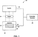
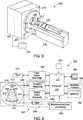
Ein Detektor mit einer gemäß verschiedenen Ausführungsformen ausgebildeten Photodiodenanordnung, Bezug nehmend auf
Der Controller/Prozessor
In verschiedenen Ausführungsformen ist der Detektor
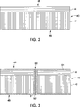
Eine Ausführungsform zur Anfertigung der Photodiodenanordnung
Der veranschaulichte Fertigungsprozess verwendet keinen Ionenimplantationsprozess zum Bilden eines Photodiodenübergangs. Außerdem wird zum Verbinden der Photodiode mit der Silizium-Durchkontaktierung (TSV) kein Metallprozess verwendet. Speziell veranschaulicht
In einer Ausführungsform ist der Siliziumwafer
Die Substratschicht
Es ist zu beachten, dass in verschiedenen Ausführungsformen, z. B. bei Verwendung des Fertigungsprozesses zum Herstellen einer kachelartig gruppierbaren zweidimensionalen (2D) frontbeleuchteten Photodiodenanordnung mit rückseitigem Anschluss, das als die Photodiodenanordnung
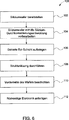
In
Danach wird die Durchkontaktierung
Die Durchkontaktierung
Danach, und wie in
Die Epi-Schicht, die eine p+-dotierte Epi-Schicht
Dann wird eine Strukturätzung ausgebildet, z. B. mithilfe einer Fotolackmaske zum Definieren von Öffnung
Das Ätzen definiert so die pixelige Anordnungsstruktur. Zusätzliche Prozesse können bereitgestellt werden, zum Beispiel unter Verwendung eines geeigneten Diffusions- oder Graben-/Ätzungsprozesses zum Isolieren benachbarter Photodioden
Danach ist nach der Fertigung der Photodiodenanordnung
Der Wafer
Dementsprechend werden in verschiedenen Ausführungsformen mithilfe von CMOS-Methoden integrierte Dioden-/Auslesebauelemente auf der Beleuchtungsseite
Es ist zu beachten, dass bei der Fertigung jede geeignete CMOS-Fertigungsmethode verwendet werden kann. Auch können die verschiedenen Schichten anhand eines beliebigen geeigneten Prozesses gebildet werden, wie z. B. u. a. Epitaxie, wie oben beschrieben, oder direktes Silizium-Silizium-Bonden. Der zum Bilden der Schichten verwendete Prozess kann sich z. B. auf die Bauelementanforderungen oder die Dicke der Schichten stützen.It should be noted that any suitable CMOS manufacturing method can be used in the manufacturing process. Also, the various layers may be formed using any suitable process, such as B. u. a. Epitaxy, as described above, or direct silicon-silicon bonding. The process used to form the layers may be e.g. B. based on the device requirements or the thickness of the layers.
Die Metallisierung
Es ist zu beachten, dass das Kanal-Layout für die Ausleseelektronik
So kann eine Ausgestaltung aus Photosensoranordnung und Ausleseelektronik bereitgestellt werden, welche die Photodiodenanordnung
In verschiedenen Ausführungsformen entsprechen die Photodioden
Verschiedene Ausführungsformen sehen ein in
Danach wird an
Die Strukturätzung der Epi-Schicht wird an
Diverse Ausführungsformen sehen also Systeme und Verfahren zur Anfertigung einer frontbeleuchteten Durchkontaktierungs-Photodiodenanordnung mit durch dotierte Epi-Abscheidung gebildeten Diodenübergängen vor. In einigen Ausführungsformen beginnt die Fertigung mit einem normalen Silizium-Epi-Wafer mit einer hochohmigen Epi-Schicht auf einem Substrat mit einem niedrigeren Widerstand. Nach der Anfertigung von Vorbearbeitungs-Silizium-Durchkontaktierungen am Epi-Wafer wird die Photodiodenanordnung durch dotierte Epi-Schichtabscheidung auf der hochohmigen Schicht mit Strukturätzungen ausgebildet. Die dotierte Epitaxie stellt auch die Verbindung zwischen dem Photodiodenpixel und dem leitenden Poly-Refill der Silizium-Durchkontaktierung bereit. Weil an der Anfertigung der Photodiodenseite kein Metallprozess beteiligt ist, stellt diese frontbeleuchtete Durchkontaktierungs-Photodiodenanordnung keinen begrenzenden Faktor für die möglichen nachfolgenden Prozesse für die andere Seite dar. Zum Beispiel können CMOS-Prozesse zur Anfertigung von Ausleseelektronikkomponenten an der anderen Seite des Wafers verwendet werden, um integrierte Photodioden- und Ausleseelektronik-Bauelemente ohne die Verwendung nicht standardmäßiger doppelseitiger Fotolitografieprozesse zu erzielen.Thus, various embodiments provide systems and methods for fabricating a front illuminated via photodiode array having diode junctions formed by doped epi-deposition. In some embodiments, fabrication begins with a standard silicon epi wafer having a high-resistance epi-layer on a lower resistance substrate. After fabrication of preprocessing silicon vias on the epi wafer, the photodiode array is formed by doped epi-layer deposition on the high resistive layer with pattern etches. The doped epitaxy also provides the connection between the photodiode pixel and the conductive poly-refill of the silicon via. Because no metal process is involved in the fabrication of the photodiode side, this front-illuminated via photodiode array is not a limiting factor for the possible subsequent processes for the other side. For example, CMOS processes may be used to fabricate readout electronics components on the other side of the wafer. to achieve integrated photodiode and readout electronics devices without the use of non-standard double-sided photolithographic processes.
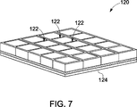
Der Siliziumwafer mit integrierter Photosensoranordnung und Ausleseelektronik kann zu kachelartig gruppierbaren 2D-Siliziumchips gestaltet werden, wie z. B. durch einen geeigneten Waferzertrennungsprozess. Danach können die kachelartig gruppierbaren Siliziumchips zum Bilden eines Detektormoduls eingehäust werden, wie z. B. eines CT-Detektormoduls, das digitale Eingänge/Ausgänge und Stromversorgungseingänge von den kachelartig gruppierbaren Siliziumchips bereitstellt.The silicon wafer with integrated photosensor array and readout electronics can be designed into tiling-like groupable 2D silicon chips, such. By a suitable wafer dicing process. Thereafter, the tiling groupable silicon chips can be housed to form a detector module, such. A CT detector module that provides digital inputs / outputs and power supply inputs from the tiling-groupable silicon chips.
Zum Beispiel kann, wie in
Die verschiedenen Ausführungsformen können in Verbindung mit verschiedenen Typen von bildgebenden Systemen realisiert werden. Zum Beispiel ist
Das multimodale bildgebende System
Das CT-Bildgebungssystem
Wie oben besprochen, beinhaltet der Detektor
Die Drehung der Gantry
Die vom Bediener eingespeisten Befehle und Parameter werden vom Computer
In einer Ausführungsform, wobei wieder auf
In der beispielhaften Ausführungsform werden die Röntgenstrahlenquelle
Oben werden Ausführungsbeispiele für ein multimodales bildgebendes System ausführlich beschrieben. Die veranschaulichten Komponenten des multimodalen bildgebenden Systems sind nicht auf die hierin beschriebenen spezifischen Ausführungsformen beschränkt, die Komponenten jedes multimodalen bildgebenden Systems können vielmehr unabhängig und separat von hierin beschriebenen anderen Komponenten genutzt werden. Zum Beispiel können die oben beschriebenen Komponenten des multimodalen bildgebenden Systems auch in Kombination mit anderen bildgebenden Systemen verwendet werden.In the above, embodiments of a multimodal imaging system will be described in detail. The illustrated components of the multimodal imaging system are not limited to the specific embodiments described herein, but the components of each multimodal imaging system may be used independently and separately from other components described herein. For example, the components of the multimodal imaging system described above may also be used in combination with other imaging systems.
Die verschiedenen Ausführungsformen und/oder Komponenten, z. B. die Module oder Komponenten und Controller in ihnen, können auch als Teil eines oder mehrerer Computer oder Prozessoren implementiert werden. Der Computer oder Prozessor kann ein Rechengerät, ein Eingabegerät, eine Anzeigeeinrichtung und eine Schnittstelle, z. B. für Zugang zum Internet, beinhalten. Der Computer oder Prozessor kann einen Mikroprozessor beinhalten. Der Mikroprozessor kann mit einem Kommunikationsbus verbunden sein. Der Computer oder Prozessor kann auch einen Speicher beinhalten. Der Speicher kann (einen) Direktzugriffsspeicher (RAM) und Festwertspeicher (ROM) beinhalten. Der Computer oder Prozessor kann ferner ein Speichergerät beinhalten, das ein Festplattenlaufwerk oder ein entfernbares Speicherlaufwerk wie ein Diskettenlaufwerk, ein optisches Laufwerk und dergleichen sein kann. Das Speichergerät kann auch eine andere ähnliche Einrichtung zum Laden von Computerprogrammen oder anderen Anweisungen in den Computer oder Prozessor sein.The various embodiments and / or components, for. The modules or components and controllers in them may also be implemented as part of one or more computers or processors. The computer or processor may include a computing device, an input device, a display device, and an interface, e.g. For access to the Internet. The computer or processor may include a microprocessor. The microprocessor may be connected to a communication bus. The computer or processor may also include memory. The memory may include Random Access Memory (RAM) and Read Only Memory (ROM). The computer or processor may further include a storage device, which may be a hard disk drive or a removable storage drive such as a floppy disk drive, an optical drive, and the like. The storage device may also be another similar device for loading computer programs or other instructions into the computer or processor.
Der hierin verwendete Begriff „Computer” oder „Modul” kann jedes beliebige System auf Prozessorbasis oder Mikroprozessorbasis sein, einschließlich Systemen, die Mikrocontroller, Reduced Instruction Set Computers (RISC), ASIC, Logikschaltungen und jede(n) beliebige(n) andere(n) Schaltung oder Prozessor verwenden, die/der zur Ausführung der hierin beschriebenen Funktionen in der Lage ist. Die obigen Beispiele sind nur veranschaulichend und sollen die Definition und/oder Bedeutung des Begriffs „Computer” in keiner Weise einschränken.As used herein, the term "computer" or "module" may be any processor-based or microprocessor-based system, including systems including microcontroller, reduced instruction set computer (RISC), ASIC, logic circuitry, and any other (n ) Use circuitry or processor capable of performing the functions described herein. The above examples are illustrative only and are not intended to limit the definition and / or meaning of the term "computer" in any way.
Der Computer oder Prozessor führt einen Satz von Befehlen aus, die in einem oder mehreren Speicherelementen gespeichert sind, um die Eingabedaten zu verarbeiten. Die Speicherelemente können, je nach Wunsch oder Bedarf, auch Daten oder andere Informationen speichern. Das Speicherelement kann die Form einer Informationsquelle oder eines physikalischen Speicherelements in einer Verarbeitungsmaschine haben.The computer or processor executes a set of instructions stored in one or more memory elements to process the input data. The storage elements may also store data or other information as desired or needed. The storage element may take the form of an information source or a physical storage element in a processing machine.
Der Befehlssatz kann verschiedene Befehle beinhalten, die den Computer oder Prozessor als eine Verarbeitungsmaschine anweisen, bestimmte Vorgänge wie die Verfahren und Prozesse der verschiedenen Ausführungsformen der Erfindung durchzuführen. Der Befehlssatz kann die Form eines Software-Programms haben, das Teil von (einem) physischen nichtflüchtigen computerlesbaren Medium oder Medien bildet. Die Software kann verschiedene Formen haben, wie z. B. System-Software oder Anwendungssoftware. Ferner kann die Software die Form einer Sammlung separater Programme oder Module, eines Programmmoduls in einem größeren Programm oder eines Teils eines Programmmoduls haben. Die Software kann auch modulare Programmierung in der Form von objektorientierter Programmierung beinhalten. Die Verarbeitung von Eingabedaten durch die Verarbeitungsmaschine kann als Reaktion auf Benutzerbefehle oder als Reaktion auf Ergebnisse früherer Verarbeitungen oder als Reaktion auf eine Anforderung von einer anderen Verarbeitungsmaschine erfolgen.The instruction set may include various instructions that instruct the computer or processor as a processing machine to perform certain operations, such as the methods and processes of the various embodiments of the invention. The instruction set may take the form of a software program that forms part of (a) physical non-transitory computer-readable medium or media. The software can take various forms, such as: For example, system software or application software. Further, the software may take the form of a collection of separate programs or modules, a program module in a larger program or part of a program module. The software may also include modular programming in the form of object-oriented programming. The processing of input data by the processing engine may be in response to user commands or in response to results of previous processing or in response to a request from another processing machine.
Die hierin verwendeten Begriffe „Software” und „Firmware” sind untereinander austauschbar und beinhalten jedes in einem Speicher gespeicherte Computerprogramm zur Ausführung durch einen Computer, einschließlich RAM-Speicher, ROM-Speicher, EPROM-Speicher, EEPROM-Speicher und nichtflüchtiger RAM-Speicher (NVRAM). Die obigen Speichertypen sind nur beispielhaft und daher bezüglich der zur Speicherung eines Computerprogramms verwendbaren Speichertypen nicht beschränkend.The terms "software" and "firmware" as used herein are interchangeable and include any computer program stored in memory for execution by a computer, including RAM, ROM, EPROM, EEPROM, and non-volatile RAM. NVRAM). The above memory types are exemplary only and therefore not limiting with respect to the types of memory usable for storing a computer program.
Es ist zu beachten, dass die obige Beschreibung zur Veranschaulichung und nicht zur Einschränkung dienen soll. Zum Beispiel können die oben beschriebenen Ausführungsformen (und/oder Aspekte derselben) in Kombination miteinander verwendet werden. Außerdem können viele Änderungen vorgenommen werden, um ein(e) besondere(s) Situation oder Material an die Lehre der verschiedenen Ausführungsformen anzupassen, ohne von ihrem Umfang abzuweichen. Zwar sind Abmessungen und Materialtypen, die hierin beschrieben werden, zur Definition der Parameter der Erfindung vorgesehen, sie sind aber in keiner Weise beschränkend und lediglich beispielhaft. Der Fachpersonen werden bei der Betrachtung der obigen Beschreibung viele weitere Ausführungsformen einfallen. Der Umfang der verschiedenen Ausführungsformen ist daher in Bezug auf die angehängten Ansprüche zusammen mit dem vollen Umfang von Äquivalenten, zu denen derartige Ansprüche berechtigt sind, zu bestimmen. In den angehängten Ansprüchen werden die Begriffe „beinhalten” und „in der/dem/denen” als einfache Äquivalente der Begriffe „aufweisend” bzw. „wobei” verwendet. Darüber hinaus werden in den folgenden Ansprüchen die Begriffe „erste”, „zweite” und „dritte” usw. lediglich als Bezeichnungen verwendet und es ist nicht vorgesehen, dass sie ihren Objekten numerische Anforderungen auferlegen. Ferner sind die Begrenzungen der folgenden Ansprüche nicht im Mittel-für-eine-Funktion-Format geschrieben und dürfen nicht auf der Basis von 35 USC § 112, sechster Absatz, ausgelegt werden, sofern derartige Anspruchsbegrenzungen nicht und bis sie ausdrücklich den Ausdruck „Mittel für” gefolgt von einer Funktionsaussage ohne weitere Struktur verwenden.It should be noted that the above description is intended to be illustrative and not limiting. For example, the above-described embodiments (and / or aspects thereof) may be used in combination with each other. In addition, many changes may be made to adapt a particular situation or material to the teachings of the various embodiments without departing from the scope thereof. While dimensions and types of materials described herein are intended to define the parameters of the invention, they are in no way limiting and merely exemplary. Those skilled in the art will come to many more embodiments when considering the above description. The scope of the various embodiments is, therefore, to be determined with reference to the appended claims, along with the full scope of equivalents to which such claims are entitled. In the appended claims, the terms "including" and "in / which" are used as simple equivalents of the terms "having" and "being", respectively. Moreover, in the following claims, the terms "first," "second," and "third," etc. are used merely as labels and are not intended to impose numerical requirements on their objects. Furthermore, the limitations of the following claims are not written in a one-to-one-for-one format and may not be construed on the basis of 35 USC § 112, sixth paragraph, unless such limitations apply and until they expressly use the term "means for Followed by a function statement without further structure.
Diese schriftliche Beschreibung verwendet Beispiele zur Offenbarung der verschiedenen Ausführungsformen, einschließlich der besten Art der Ausführung, und auch, um einer Fachperson die Ausübung der verschiedenen Ausführungsformen zu ermöglichen, einschließlich der Herstellung und Benutzung jedweder Vorrichtungen oder Systeme und der Durchführung eingebundener Verfahren. Der patentfähige Umfang der verschiedenen Ausführungsformen wird durch die Ansprüche definiert und kann weitere Beispiele beinhalten, die der Fachperson einfallen werden. Es ist vorgesehen, dass derartige weitere Beispiele in den Umfang der Ansprüche fallen, wenn die Beispiele strukturelle Elemente haben, die sich nicht von der wörtlichen Sprache der Ansprüche unterscheiden, oder wenn die Beispiele äquivalente strukturelle Elemente mit unwesentlichen Unterschieden von den wörtlichen Sprachen der Ansprüche beinhalten.This written description uses examples to disclose the various embodiments, including the best mode of execution, and also to enable one skilled in the art to practice the various embodiments, including making and using any devices or systems and performing integrated methods. The patentable scope of the various embodiments is defined by the claims, and may include other examples that occur to those skilled in the art. It is intended that such further examples fall within the scope of the claims if the examples have structural elements that do not differ from the literal language of the claims, or if the examples include equivalent structural elements with insubstantial differences from the literal languages of the claims ,
Es sind Photodiodenanordnungen und Fertigungsverfahren vorgesehen. Eine Photodiodenanordnung beinhaltet einen Siliziumwaffer mit einer ersten Oberfläche und einer gegenüberliegenden zweiten Oberfläche und eine Vielzahl von leitenden Durchkontaktierungen durch den Siliziumwafer. Die Photodiodenanordnung beinhaltet ferner eine dotierte epitaktische Schicht auf der ersten Oberfläche, wobei die dotierte epitaktische Schicht und das Substrat eine Vielzahl von Diodenübergängen bilden. Eine Strukturätzung definiert eine Anordnung der Diodenübergänge.There are provided photodiode arrays and manufacturing processes. A photodiode array includes a silicon wafer having a first surface and an opposing second surface and a plurality of conductive vias through the silicon wafer. The photodiode array further includes a doped epitaxial layer on the first surface, wherein the doped epitaxial layer and the substrate form a plurality of diode junctions. A structure etch defines an array of diode junctions.
Claims (20)
Applications Claiming Priority (2)
| Application Number | Priority Date | Filing Date | Title |
|---|---|---|---|
| US13/343,165 | 2012-01-04 | ||
| US13/343,165 US8736008B2 (en) | 2012-01-04 | 2012-01-04 | Photodiode array and methods of fabrication |
Publications (1)
| Publication Number | Publication Date |
|---|---|
| DE102012113168A1 true DE102012113168A1 (en) | 2013-07-04 |
Family
ID=48608049
Family Applications (1)
| Application Number | Title | Priority Date | Filing Date |
|---|---|---|---|
| DE102012113168A Withdrawn DE102012113168A1 (en) | 2012-01-04 | 2012-12-28 | Photodiode arrays and manufacturing processes |
Country Status (3)
| Country | Link |
|---|---|
| US (1) | US8736008B2 (en) |
| JP (1) | JP6133055B2 (en) |
| DE (1) | DE102012113168A1 (en) |
Cited By (1)
| Publication number | Priority date | Publication date | Assignee | Title |
|---|---|---|---|---|
| WO2014166707A1 (en) * | 2013-04-11 | 2014-10-16 | Siemens Aktiengesellschaft | Production method of a sensor chip and computerized tomography detector |
Families Citing this family (11)
| Publication number | Priority date | Publication date | Assignee | Title |
|---|---|---|---|---|
| US8901697B2 (en) * | 2012-03-16 | 2014-12-02 | Analog Devices, Inc. | Integrated circuit having a semiconducting via; an integrated circuit including a sensor, such as a photosensitive device, and a method of making said integrated circuit |
| EP3069170B1 (en) | 2013-11-15 | 2020-04-15 | Koninklijke Philips N.V. | Double-sided organic photodetector on flexible substrate |
| JP2015133408A (en) | 2014-01-14 | 2015-07-23 | 株式会社島津製作所 | radiation detector |
| TWI621254B (en) * | 2014-12-19 | 2018-04-11 | G射線瑞士公司 | Monolithic cmos integrated pixel detector, and systems and methods for particle detection and imaging including various applications |
| US9754992B2 (en) | 2015-01-21 | 2017-09-05 | Terapede Systems Inc. | Integrated scintillator grid with photodiodes |
| JP6725231B2 (en) * | 2015-10-06 | 2020-07-15 | ソニーセミコンダクタソリューションズ株式会社 | Solid-state image sensor and electronic device |
| US10522532B2 (en) * | 2016-05-27 | 2019-12-31 | Taiwan Semiconductor Manufacturing Co., Ltd. | Through via extending through a group III-V layer |
| WO2017213622A1 (en) * | 2016-06-06 | 2017-12-14 | Terapede Systems Inc. | Integrated scintillator grid with photodiodes |
| KR102635858B1 (en) * | 2017-01-05 | 2024-02-15 | 삼성전자주식회사 | Image sensor |
| EP3723138A1 (en) * | 2019-04-10 | 2020-10-14 | ams International AG | Optoelectronic device, photonic detector and method of producing an optoelectronic device |
| US11874409B2 (en) | 2020-07-06 | 2024-01-16 | Canon Medical Systems Corporation | Correction X-ray detector, X-ray CT apparatus, and detector element determining method |
Family Cites Families (27)
| Publication number | Priority date | Publication date | Assignee | Title |
|---|---|---|---|---|
| US5886353A (en) | 1995-04-21 | 1999-03-23 | Thermotrex Corporation | Imaging device |
| US6133615A (en) * | 1998-04-13 | 2000-10-17 | Wisconsin Alumni Research Foundation | Photodiode arrays having minimized cross-talk between diodes |
| US6667528B2 (en) * | 2002-01-03 | 2003-12-23 | International Business Machines Corporation | Semiconductor-on-insulator lateral p-i-n photodetector with a reflecting mirror and backside contact and method for forming the same |
| GB0201260D0 (en) | 2002-01-21 | 2002-03-06 | Europ Org For Nuclear Research | A sensing and imaging device |
| US7291782B2 (en) * | 2002-06-22 | 2007-11-06 | Nanosolar, Inc. | Optoelectronic device and fabrication method |
| GB2392307B8 (en) * | 2002-07-26 | 2006-09-20 | Detection Technology Oy | Semiconductor structure for imaging detectors |
| JP4440554B2 (en) * | 2002-09-24 | 2010-03-24 | 浜松ホトニクス株式会社 | Semiconductor device |
| US7214999B2 (en) * | 2003-10-31 | 2007-05-08 | Motorola, Inc. | Integrated photoserver for CMOS imagers |
| US6943409B1 (en) * | 2004-05-24 | 2005-09-13 | International Business Machines Corporation | Trench optical device |
| WO2005122285A2 (en) | 2004-06-04 | 2005-12-22 | The Board Of Trustees Of The University Of Illinois | Methods and devices for fabricating and assembling printable semiconductor elements |
| WO2006111869A2 (en) | 2005-04-22 | 2006-10-26 | Koninklijke Philips Electronics N.V. | Pet/mr scanner with time-of-flight capability |
| DE102005026242B4 (en) * | 2005-06-07 | 2007-05-03 | Austriamicrosystems Ag | Photodiode with semiconductor integrated circuit and method of manufacture |
| US7759680B2 (en) | 2005-11-30 | 2010-07-20 | General Electric Company | Thin-film transistor and diode array for an imager panel or the like |
| US7576404B2 (en) * | 2005-12-16 | 2009-08-18 | Icemos Technology Ltd. | Backlit photodiode and method of manufacturing a backlit photodiode |
| US7378309B2 (en) * | 2006-03-15 | 2008-05-27 | Sharp Laboratories Of America, Inc. | Method of fabricating local interconnects on a silicon-germanium 3D CMOS |
| WO2007127607A1 (en) | 2006-04-25 | 2007-11-08 | Koninklijke Philips Electronics, N.V. | Implementation of avalanche photo diodes in (bi) cmos processes |
| TW200818534A (en) * | 2006-08-10 | 2008-04-16 | Icemos Technology Corp | Method of manufacturing a photodiode array with through-wafer vias |
| GB2441814B (en) | 2006-09-07 | 2012-04-11 | Detection Technology Oy | Photodiode array output signal multiplexing |
| KR101519038B1 (en) | 2007-01-17 | 2015-05-11 | 더 보오드 오브 트러스티스 오브 더 유니버시티 오브 일리노이즈 | Optical systems fabricated by printing-based assembly |
| JP4825778B2 (en) * | 2007-11-16 | 2011-11-30 | 株式会社日立製作所 | Semiconductor device and manufacturing method thereof |
| ITTO20080045A1 (en) | 2008-01-18 | 2009-07-19 | St Microelectronics Srl | PLACE OF PHOTODIODS OPERATING IN GEIGER MODES MUTUALLY INSULATED AND RELATIVE PROCESS OF MANUFACTURING |
| US20100108893A1 (en) * | 2008-11-04 | 2010-05-06 | Array Optronix, Inc. | Devices and Methods for Ultra Thin Photodiode Arrays on Bonded Supports |
| EP2380038B1 (en) | 2008-12-22 | 2019-01-09 | Koninklijke Philips N.V. | Cmos imager |
| US8409908B2 (en) | 2009-07-30 | 2013-04-02 | General Electric Company | Apparatus for reducing photodiode thermal gain coefficient and method of making same |
| JP2011044717A (en) * | 2009-08-20 | 2011-03-03 | Icemos Technology Ltd | Direct wafer-bonded through-hole photodiode |
| EP2583312A2 (en) | 2010-06-18 | 2013-04-24 | Sionyx, Inc. | High speed photosensitive devices and associated methods |
| US9097809B2 (en) | 2011-06-30 | 2015-08-04 | Carestream Health, Inc. | Radiographic detector including trap occupancy change monitor and feedback, imaging apparatus and methods using the same |
-
2012
- 2012-01-04 US US13/343,165 patent/US8736008B2/en active Active
- 2012-12-27 JP JP2012283969A patent/JP6133055B2/en active Active
- 2012-12-28 DE DE102012113168A patent/DE102012113168A1/en not_active Withdrawn
Cited By (1)
| Publication number | Priority date | Publication date | Assignee | Title |
|---|---|---|---|---|
| WO2014166707A1 (en) * | 2013-04-11 | 2014-10-16 | Siemens Aktiengesellschaft | Production method of a sensor chip and computerized tomography detector |
Also Published As
| Publication number | Publication date |
|---|---|
| JP6133055B2 (en) | 2017-05-24 |
| US8736008B2 (en) | 2014-05-27 |
| JP2013140975A (en) | 2013-07-18 |
| US20130168750A1 (en) | 2013-07-04 |
Similar Documents
| Publication | Publication Date | Title |
|---|---|---|
| DE102012113168A1 (en) | Photodiode arrays and manufacturing processes | |
| DE102012112981A1 (en) | Photodiode arrays and methods of manufacture | |
| US8798229B2 (en) | Detector modules and methods of manufacturing | |
| US9087755B2 (en) | Photodiodes and fabrication thereof | |
| DE102016208343B4 (en) | Optical sensor device and method for producing the optical sensor device | |
| EP3507835B1 (en) | Electromagnetic radiation detector comprising charge transport across a bonded interface | |
| DE102018124677A1 (en) | SPAD image sensor and related manufacturing process | |
| DE102011079589A1 (en) | Unit pixel for a photodetection device | |
| DE102006056995B4 (en) | Contact transitions for transistor and diode array in thin film technology for an imaging panel or the like | |
| DE102010043822B4 (en) | Photodiode and photodiode array and method for their operation | |
| DE112016004224T5 (en) | A solid state imaging device, electronic device, and method of manufacturing the solid state imaging device | |
| DE102014003068B4 (en) | PROCESS FOR PREPARING AN IMAGEER AND IMAGING APPARATUS | |
| DE112017000381T5 (en) | A detector device with majority current and isolation means | |
| DE102007044728A1 (en) | Interface arrangement and method for integrating a data acquisition system on a sensor matrix | |
| DE102009047202A1 (en) | detector | |
| DE102019103721A1 (en) | Image sensor for capturing LED light with reduced flicker | |
| DE112015007248T5 (en) | DETECTOR ARRANGEMENT FOR RADIATION IMAGING METHOD | |
| DE112021006393T5 (en) | Photodiode device with improved properties | |
| DE102020209822A1 (en) | SENSOR AND METHOD OF FORMING THE SAME | |
| DE102016125331B4 (en) | Matched flat panel X-ray detector, matched light imaging panel and method of making a light imaging panel | |
| DE102006060913A1 (en) | Image sensor, control method for this, X-ray detector and X-ray CT apparatus | |
| DE102009043256A1 (en) | Image sensor and method for its production | |
| DE102011083689A1 (en) | Flat panel X-ray detector has X-ray converter for conversion of X-rays and active matrix of pixel elements for detecting and reading converted X-radiation, where sensitive surface of active matrix is circular or semicircular | |
| DE102016114804B4 (en) | Semiconductor device and method for manufacturing the same | |
| DE102022124036A1 (en) | Photoelectric conversion device, photoelectric conversion system and moving body |
Legal Events
| Date | Code | Title | Description |
|---|---|---|---|
| R082 | Change of representative |
Representative=s name: RUEGER, BARTHELT & ABEL PATENTANWAELTE, DE Representative=s name: RUEGER ] ABEL PATENT- UND RECHTSANWAELTE, DE Representative=s name: RUEGER ABEL PATENT- UND RECHTSANWAELTE, DE |
|
| R012 | Request for examination validly filed | ||
| R119 | Application deemed withdrawn, or ip right lapsed, due to non-payment of renewal fee |