DE102007018456A1 - Aryl- and / or heteroaryl-substituted main group element halides and / or pseudohalides, use of main group element halides and / or pseudohalides, organic semiconductive matrix material, electronic and optoelectronic devices - Google Patents
Aryl- and / or heteroaryl-substituted main group element halides and / or pseudohalides, use of main group element halides and / or pseudohalides, organic semiconductive matrix material, electronic and optoelectronic devices Download PDFInfo
- Publication number
- DE102007018456A1 DE102007018456A1 DE102007018456A DE102007018456A DE102007018456A1 DE 102007018456 A1 DE102007018456 A1 DE 102007018456A1 DE 102007018456 A DE102007018456 A DE 102007018456A DE 102007018456 A DE102007018456 A DE 102007018456A DE 102007018456 A1 DE102007018456 A1 DE 102007018456A1
- Authority
- DE
- Germany
- Prior art keywords
- aryl
- heteroaryl
- pseudohalides
- main group
- group element
- Prior art date
- Legal status (The legal status is an assumption and is not a legal conclusion. Google has not performed a legal analysis and makes no representation as to the accuracy of the status listed.)
- Granted
Links
Classifications
-
- C—CHEMISTRY; METALLURGY
- C07—ORGANIC CHEMISTRY
- C07F—ACYCLIC, CARBOCYCLIC OR HETEROCYCLIC COMPOUNDS CONTAINING ELEMENTS OTHER THAN CARBON, HYDROGEN, HALOGEN, OXYGEN, NITROGEN, SULFUR, SELENIUM OR TELLURIUM
- C07F9/00—Compounds containing elements of Groups 5 or 15 of the Periodic System
- C07F9/90—Antimony compounds
- C07F9/92—Aromatic compounds
-
- H—ELECTRICITY
- H10—SEMICONDUCTOR DEVICES; ELECTRIC SOLID-STATE DEVICES NOT OTHERWISE PROVIDED FOR
- H10K—ORGANIC ELECTRIC SOLID-STATE DEVICES
- H10K71/00—Manufacture or treatment specially adapted for the organic devices covered by this subclass
- H10K71/30—Doping active layers, e.g. electron transporting layers
-
- H—ELECTRICITY
- H10—SEMICONDUCTOR DEVICES; ELECTRIC SOLID-STATE DEVICES NOT OTHERWISE PROVIDED FOR
- H10K—ORGANIC ELECTRIC SOLID-STATE DEVICES
- H10K85/00—Organic materials used in the body or electrodes of devices covered by this subclass
- H10K85/30—Coordination compounds
- H10K85/311—Phthalocyanine
-
- H—ELECTRICITY
- H10—SEMICONDUCTOR DEVICES; ELECTRIC SOLID-STATE DEVICES NOT OTHERWISE PROVIDED FOR
- H10K—ORGANIC ELECTRIC SOLID-STATE DEVICES
- H10K85/00—Organic materials used in the body or electrodes of devices covered by this subclass
- H10K85/60—Organic compounds having low molecular weight
- H10K85/631—Amine compounds having at least two aryl rest on at least one amine-nitrogen atom, e.g. triphenylamine
- H10K85/633—Amine compounds having at least two aryl rest on at least one amine-nitrogen atom, e.g. triphenylamine comprising polycyclic condensed aromatic hydrocarbons as substituents on the nitrogen atom
-
- Y—GENERAL TAGGING OF NEW TECHNOLOGICAL DEVELOPMENTS; GENERAL TAGGING OF CROSS-SECTIONAL TECHNOLOGIES SPANNING OVER SEVERAL SECTIONS OF THE IPC; TECHNICAL SUBJECTS COVERED BY FORMER USPC CROSS-REFERENCE ART COLLECTIONS [XRACs] AND DIGESTS
- Y02—TECHNOLOGIES OR APPLICATIONS FOR MITIGATION OR ADAPTATION AGAINST CLIMATE CHANGE
- Y02E—REDUCTION OF GREENHOUSE GAS [GHG] EMISSIONS, RELATED TO ENERGY GENERATION, TRANSMISSION OR DISTRIBUTION
- Y02E10/00—Energy generation through renewable energy sources
- Y02E10/50—Photovoltaic [PV] energy
- Y02E10/549—Organic PV cells
Abstract
Die Erfindung betrifft Aryl- und/oder Heteroaryl-substituierte Hauptgruppenelementhalogenide und/oder -pseudohalogenide, die Verwendung von Hauptgruppenelementhalogeniden und -pseudohalogeniden als Dotand zur Dotierung eines organischen halbleitenden Matrixmaterials, als Ladungsinjektionsschicht, als Löcherblockerschicht, als Elektrodenmaterial, als Transportmaterial selbst, als Speichermaterial in elektronischen oder optoelektronischen Bauelementen sowie ein organisches halbleitendes Material und elektronische oder optoelektronische Bauelemente.The invention relates to aryl- and / or heteroaryl-substituted main group element halides and / or pseudohalides, the use of Hauptgruppenelementhalogeniden and pseudohalides as dopant for doping an organic semiconducting matrix material, as a charge injection layer, as a hole blocker layer, as an electrode material, as a transport material itself, as a memory material in electronic or optoelectronic components and an organic semiconducting material and electronic or optoelectronic components.
Description
Die Erfindung betrifft Aryl- und/oder Heteroaryl-substituierte Hauptgruppenelementhalogenide und/oder -pseudohalogenide, die Verwendung von Hauptgruppenelementhalogeniden und/oder -pseudohalogeniden als Dotand zur Dotierung eines organischen halbleitenden Matrixmaterials, als Ladungsinjektionsschicht, als Löcherblockerschicht, als Elektrodenmaterial, als Transportmaterial selbst, als Speichermaterial in elektronischen oder optoelektronischen Bauelementen, sowie ein organisches halbleitendes Material und elektronische oder optoelektronische Bauelemente.The The invention relates to aryl- and / or heteroaryl-substituted main group element halides and / or pseudohalides, the use of main group element halides and / or pseudohalides as dopant for doping an organic Semiconductor matrix material, as a charge injection layer, as Hole blocker layer, as electrode material, as transport material itself, as storage material in electronic or optoelectronic components, as well as an organic semiconducting material and electronic or optoelectronic components.
Es
ist bekannt organische Halbleiter durch Dotierung hinsichtlich ihrer
elektrischen Eigenschaften, insbesondere ihrer elektrischen Leitfähigkeit
zu verändern, wie dies auch bei anorganischen Halbleitern
wie Siliciumhalbleitern der Fall ist. Hierbei wird durch Erzeugung
von Ladungsträgern im Matrixmaterial eine Erhöhung
der zunächst recht niedrigen Leitfähigkeit sowie
je nach Art des verwendeten Dotanden eine Veränderung im
Fermi-Niveau des Halbleiters erreicht. Eine Dotierung führt
hierbei zu einer Erhöhung der Leitfähigkeit von
Ladungstransportschichten, wodurch ohmsche Verluste verringert werden,
und zu einem verbesserten Übergang der Ladungsträger
zwischen Kontakten und organischer Schicht. Anorganische Dotanden
wie Alkalimetalle (z. B. Cäsium) oder Lewis-Säuren
(z. B. FeCl3; SbCl5)
sind bei organischen Matrixmaterialien aufgrund ihrer hohen Diffusionskoeffizienten
meist nachteilig, da die Funktion und Stabilität der elektronischen Bauelemente
beeinträchtigt wird, siehe
Der vorliegenden Erfindung liegt die Aufgabe zugrunde, Verbindungen bereitzustellen, die als Dotand, als Ladungsinjektionsschicht, als Löcherblockerschicht, als Elektrodenmaterial, als Transportmaterial selbst oder als Speichermaterial eingesetzt werden können. Vorzugsweise sollen die Verbindungen ausreichend hohe Reduktionspotentiale aufweisen, ohne störende Einflüsse auf das Matrixmaterial sein und eine wirksame Erhöhung der Ladungsträgeranzahl im Matrixmaterial bereitstellen und vergleichsweise einfach handhabbar sein.Of the present invention has for its object, compounds to be prepared as a dopant, as a charge injection layer, as Hole blocker layer, as electrode material, as transport material itself or as a storage material can be used. Preferably, the compounds should have sufficiently high reduction potentials have, without disturbing influences on the matrix material and an effective increase in the number of charge carriers provide in the matrix material and be relatively easy to handle.
Weitere Aufgaben der vorliegenden Erfindung liegen in der Verwendung von entsprechenden Verbindungen als Dotand zur Dotierung eines organischen halbleitenden Matrixmaterials, als Ladungsinjektionsschicht, als Elektrodenmaterial, als Transportmaterial selbst sowie als Speichermaterial in elektronischen oder optoelektronischen Bauelementen, sowie in der Bereitstellung von organischen halbleitenden Materialien und von elektronischen Bauelementen oder optoelektronischen Bauelementen, in denen die offenbarten Verbindungen verwendet werden können.Further Objects of the present invention are the use of corresponding compounds as a dopant for doping an organic Semiconductor matrix material, as a charge injection layer, as Electrode material, as a transport material itself as well as storage material in electronic or optoelectronic components, as well as in the provision of organic semiconducting materials and of electronic components or optoelectronic components, in which the disclosed compounds can be used.
Die erste Aufgabe wird durch die Verbindungen gemäß Anspruch 1 gelöst. Die weiteren Aufgaben werden durch die Gegenstände der weiteren unabhängigen Ansprüche gelöst, während bevorzugte Ausführungsformen in den Unteransprüchen wiedergegeben sind.The The first object is achieved by the compounds according to claim 1 solved. The other tasks are performed by the objects the further independent claims, while preferred embodiments in the subclaims are reproduced.
In bezug auf die in den Ansprüchen gezeigte Struktur der Hauptgruppenelementhalogenide bzw. -pseudohalogenide ist festzuhalten, daß diese Verbindungen zumindest einen Rest R aufweisen, so daß n > 1 ist.In relating to the structure of main group element halides shown in the claims or pseudohalides is to be noted that these compounds have at least one radical R, so that n> 1.
Entsprechend
der Wertigkeit der Hauptgruppenelemente können zum Beispiel
folgende Unterstrukturen unter die in den Ansprüchen gezeigte
Struktur fallen:
Wenn das Zentralatom M beispielsweise S, Se
oder Te ist, so kann sich eine Struktur R1 -6-M-X0-5 ergeben. Wenn
das Zentralatom M beispielsweise P, As, Sb oder Bi ist, so kann
sich eine Struktur R1- 5-M-X0-4 ergeben. Wenn das Zentralatom M beispielsweise
Al, Ga, In, Tl, P, As, Sb oder Bi ist, ergibt sich eine Unterstruktur R1 -3-M-X0- 2. Wenn das Zentralatom M beispielsweise
Si, Sn, S, Se, Te oder Pb ist, ergibt sich eine Unterstruktur R1-4-M-X0-3.For example, according to the valence of the main group elements, the following substructures may fall within the structure shown in the claims:
If the central atom M is, for example, S, Se or Te, a structure R 1 -6 -M- X 0-5 can result. When the central atom M, for example, P, As, Sb or Bi, so a structure R 5 1- -MX 0-4 can result. When the central atom M, for example, Al, Ga, In, Tl, P, As, Sb or Bi, results in a sub-structure R 1 -3 -MX 0-. 2 If the central atom M is, for example, Si, Sn, S, Se, Te or Pb, a substructure R 1-4 -MX 0-3 results.
Diese Aryl- und/oder Heteroaryl-substituierten Hauptgruppenelementhalogenide bzw. -pseudohalogenide können auch als Löcherinjektionsschicht eingesetzt werden. So kann beispielsweise eine Schichtstruktur Anode/Akzeptor/Löchertransporter hergestellt werden. Da bei kann der Löchertransporter eine reine Schicht oder eine Mischschicht sein. Insbesondere kann der Löchertransporter ebenfalls mit einem Akzeptor dotiert sein. Die Anode kann beispielsweise ITO sein. Die Akzeptorschicht kann beispielsweise 0.5–100 nm dick sein.These Aryl- and / or heteroaryl-substituted main group element halides or pseudohalides can also be used as a hole injection layer be used. Thus, for example, a layer structure anode / acceptor / hole transporter getting produced. Since at the hole transporter a be pure layer or a mixed layer. In particular, the Hole transporter may also be doped with an acceptor. The anode may be, for example, ITO. The acceptor layer can for example 0.5-100 nm thick.
Überraschenderweise wurde festgestellt, daß bei erfindungsgemäßer Verwendung der offenbarten Hauptgruppenelementhalogenide bzw. -pseudohalogenide ein wesentlich stärkerer und/oder stabilerer Dotand als bei bisher bekannten Akzeptorverbindungen vorliegt, wobei die Hauptgruppenelementhalogenide bzw. -pseudohalogenide in neutraler Form als p-Dotand gegenüber einem organischen halbleitenden Matrixmaterial eingesetzt werden. Das oben Gesagte gilt insbesondere für Aryl- und/oder Heteroaryl-substituierte Hauptgruppenelementhalogenide bzw. -pseudohalogenide. Insbesondere wird die Leitfähigkeit von Ladungstransportschichten bei erfindungsgemäßer Verwendung wesentlich erhöht und/oder der Übergang der Ladungsträger zwischen den Kontakten und organischer Schicht bei Anwendungen als elektronisches Bauelement wesentlich verbessert. Ohne durch diese Vorstellung eingeschränkt zu sein, wird davon ausgegangen, dass bei erfindungsgemäßer Verwendung der Hauptgruppenelementhalogenide bzw. -pseudohalogenide in einer dotierten Schicht CT-Komplexe gebildet werden, insbesondere durch den Transfer von mindestens einem Elektron vom jeweiligen umgebenden Matrixmaterial. Ebenso werden dabei Kationen des Matrixmaterials gebildet, die auf dem Matrixmaterial beweglich sind. Auf diese Weise gewinnt das Matrixmaterial eine Leitfähigkeit, die gegenüber der Leitfähigkeit des undotierten Matrixmaterials erhöht ist. Leitfähigkeiten von undotierten Matrixmaterialien sind in der Regel < 10–8 S/cm, insbesondere häufig < 10–10 S/cm. Es ist dabei darauf zu achten, dass die Matrixmaterialien eine genügend hohe Reinheit aufweisen. Solche Reinheiten sind mit herkömmlichen Methoden, zum Beispiel Gradientensublimation zu erreichen. Durch Dotierung lässt sich die Leitfähigkeit solcher Matrixmaterialien auf größer 10–8 S/cm, häufig > 10–5 S/cm erhöhen. Dies gilt insbesondere für Matrixmaterialien, die ein Oxidationspotential von größer als –0,5 V vs. Fc/Fc+, bevorzugt größer 0 V vs. Fc/Fc+, insbesondere größer +0.2 V vs. Fc/Fc+ aufweisen. Die Angabe Fc/Fc+ bezieht sich auf ein Redoxpaar Ferrocen/Ferrocenium, das als Referenz in einer elektrochemischen Potentialbestimmung, zum Beispiel Zyklovoltammetrie, eingesetzt wird.Surprisingly, it has been found that in the inventive use of the disclosed Hauptgruppenelementhalogenide or pseudohalides a much stronger and / or more stable dopant than presently known acceptor is present, the main group element halides or pseudohalides used in neutral form as a p-dopant over an organic semiconducting matrix material become. The above applies in particular to aryl- and / or heteroaryl-substituted main group element halides or pseudohalides. In particular, the conductivity of charge transport layers in the case of use according to the invention is substantially increased and / or the transfer of the charge carriers between the contacts and the organic layer is substantially improved in applications as an electronic component. Without being limited by this idea, it is assumed that in the inventive use of Hauptgruppenelementhalogenide or pseudohalides in a doped layer CT complexes are formed, in particular by the transfer of at least one electron from the respective surrounding matrix material. Likewise, cations of the matrix material are formed, which are movable on the matrix material. In this way, the matrix material acquires a conductivity that is increased compared to the conductivity of the undoped matrix material. Conductivities of undoped matrix materials are generally <10 -8 S / cm, in particular frequently <10 -10 S / cm. It is important to ensure that the matrix materials have a sufficiently high purity. Such purities can be achieved by conventional methods, for example gradient sublimation. By doping, the conductivity of such matrix materials can be increased to greater than 10 -8 S / cm, often> 10 -5 S / cm. This is especially true for matrix materials that have an oxidation potential greater than -0.5 V vs. Fc / Fc + , preferably greater than 0 V vs. Fc / Fc + , in particular greater +0.2 V vs. Fc / Fc + exhibit. The term Fc / Fc + refers to a redox couple ferrocene / ferrocenium, which is used as reference in an electrochemical determination of potential, for example cyclic voltammetry.
Erfindungsgemäß wurde ferner festgestellt, daß insbesondere die beschriebenen Aryl- und/oder Heteroaryl-substituierten Hauptgruppenelementhalogenide bzw. -pseudohalogenide auch als Injektionsschicht in elektronischen Bauteilen, vorzugsweise zwischen einer Elektrode und einer Halbleiterschicht, die auch dotiert sein kann, oder auch als Blockerschicht, vorzugsweise zwischen Emitter- und Transportschicht in elektronischen Bauelementen eingesetzt werden können. Die erfindungsgemäß eingesetzten Verbindungen weisen eine überraschend hohe Stabilität in Bezug auf ihre Reaktivität mit der Atmosphäre auf.According to the invention was it also states that in particular those described Aryl- and / or heteroaryl-substituted main group element halides or pseudohalides also as an injection layer in electronic Components, preferably between an electrode and a semiconductor layer, which may also be doped, or as a blocking layer, preferably between emitter and transport layer in electronic components can be used. The inventively used Compounds have a surprisingly high stability in terms of their reactivity with the atmosphere on.
Darstellung der Aryl- und/oder Heteroaryl-substituierten Hauptgruppenelementhalogenide bzw. -pseudohalogenideRepresentation of aryl- and / or heteroaryl-substituted Main group element halides or pseudohalides
Die
beschriebenen Aryl- und/oder Heteroaryl-substituierten Hauptgruppenelementhalogenide
bzw. -pseudohalogenide lassen sich nach bekannten Verfahren synthetisieren.
Die Synthese solcher Verbindungen ist beispielsweise in folgenden
Literaturstellen beschrieben, die hiermit jeweils vollumfänglich
als Referenz in der Anmeldung mit eingeschlossen sind. Es versteht
sich, dass die genannten Literaturstellen nur beispielhaft angegeben
sind. Die Darstellung von Alkyl- und/oder Heteroalkyl-substituierten
Verbindungen ergibt sich in analoger Weise. Nach O. Glemser et al.
lassen sich z. B. Trisarylverbindungen des Arsens, des Phosphors
und des Antimons aus den entsprechenden Grignardverbindungen und
den Hauptgruppentrichloriden darstellen,
Synthese von Triaryl- bzw. -heteroarylantimondichloridenSynthesis of triaryl or heteroarylantimondichlorides
Synthese von Tris(pentafluorphenyl)antimondichloridSynthesis of tris (pentafluorophenyl) antimony dichloride
Zu einer Lösung von 1,5 mmol Tris(pentafluorphenyl)stilben in 10 ml Acetonitril wird unter Rühren bei Raumtemperatur ein Gemisch aus 1,5 mmol Iodchlorid und 10 ml Acetonitril langsam zugetropft. Aus der braunen Lösung wurde nach Etherzugabe in 65% Ausbeute das weiße kristalline Produkt erhalten. Fp.: 242–4°CTo a solution of 1.5 mmol tris (pentafluorophenyl) stilbene in 10 ml of acetonitrile is stirred at room temperature a mixture of 1.5 mmol of iodine chloride and 10 ml of acetonitrile slowly dropwise. The brown solution became ether after addition in 65% yield the white crystalline product was obtained. Mp .: 242-4 ° C
Synthese von Tris(tetrafluorpyridyl)antimondichloridSynthesis of tris (tetrafluoropyridyl) antimony dichloride
Zu einer Lösung von 1,5 mmol Tris(tetrafluorpyridyl)stilben in 10 ml Acetonitril wird unter Rühren bei Raumtemperatur ein Gemisch aus 1,5 mmol Iodchlorid und 10 ml Acetonitril langsam zugetropft. Aus der braunen Lösung wurde nach Etherzugabe in 72% Ausbeute das weiße kristalline Produkt erhalten. Fp.: 246–7°CTo a solution of 1.5 mmol tris (tetrafluoropyridyl) stilbene in 10 ml of acetonitrile is stirred at room temperature a mixture of 1.5 mmol of iodine chloride and 10 ml of acetonitrile slowly dropwise. The brown solution became ether after addition obtained in 72% yield the white crystalline product. Mp .: 246-7 ° C
Dotierungendowment
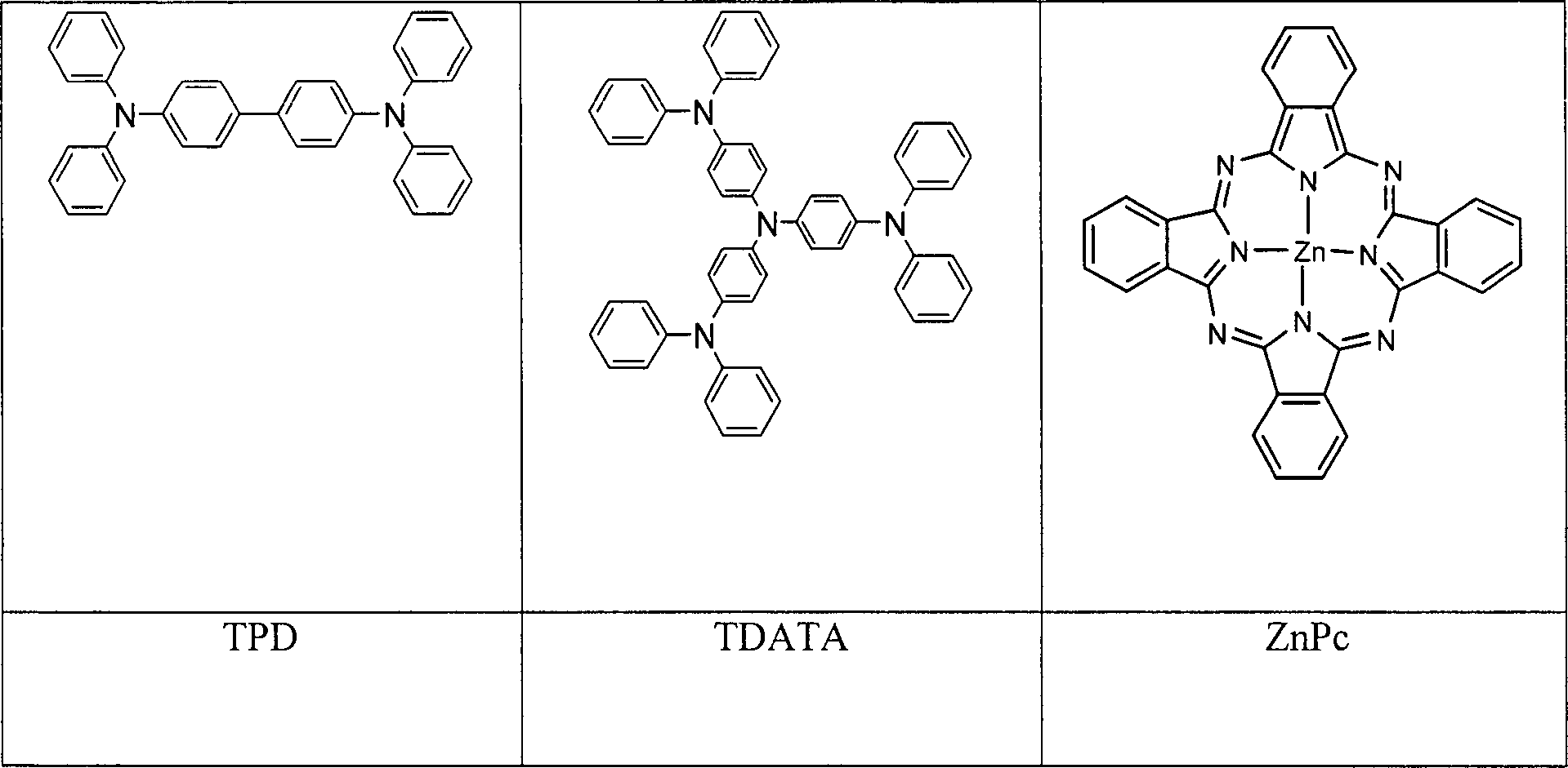
Als p-dotierbare Matrixmaterialen können unter anderem Phthalocyaninkomplexe, beispielsweise des Zn (ZnPc), Cu (CuPc), Ni (NiPc) oder anderer Metalle, wobei der Phthalocyaninligand auch substituiert sein kann, eingesetzt werden. Auch andere Metallkomplexe von Naphtocyaninen und Porphyrinen können gegebenenfalls eingesetzt werden. Weiterhin können als Matrixmaterial auch arylierte oder heteroarylierte Amine bzw. Benzidinderivate eingesetzt werden, die substituiert oder unsubstituiert sein können, beispielsweise TPD, a-NPD, TDATA, insbesondere auch Spiro-verknüpfte wie z. B. Spiro-TTB. Insbesondere können a-NPD und Spiro-TTB als Matrixmaterial eingesetzt werden.When p-dopable matrix materials may include phthalocyanine complexes, for example, Zn (ZnPc), Cu (CuPc), Ni (NiPc) or others Metals, wherein the phthalocyanine ligand may also be substituted, be used. Also other metal complexes of naphthocyanines and porphyrins may optionally be used. Furthermore, as matrix material also arylated or heteroarylated amines or benzidine derivatives are used, the substituted or unsubstituted, for example TPD, a-NPD, TDATA, especially spiro-linked as well z. B. Spiro-TTB. In particular, a-NPD and spiro-TTB be used as matrix material.
Als Matrixmaterial können neben polyaromatischen Kohlenwasserstoffen auch Heteroaromaten wie insbesondere Imidazol, Thiophen, Thiazolderivate, Heterotriphenylene aber auch andere eingesetzt werden, gegebenenfalls auch dimere, oligomere bzw. polymere Heteroaromaten. Die Heteroaromaten sind vorzugsweise substituiert, insbesondere Aryl-substituiert, beispielsweise Phenyl- oder Naphthyl-substituiert. Sie können auch als Spiroverbindungen vorliegen.When Matrix material can in addition to polyaromatic hydrocarbons also heteroaromatics, in particular imidazole, thiophene, thiazole derivatives, Heterotriphenylenes but others are used, if appropriate also dimeric, oligomeric or polymeric heteroaromatics. The heteroaromatics are preferably substituted, in particular aryl-substituted, for example, phenyl or naphthyl substituted. You can also present as spiro compounds.
Es versteht sich, dass die genannten Matrixmaterialien auch untereinander oder mit anderen Materialien gemischt im Rahmen der Erfindung einsetzbar sind. Es versteht sich, dass auch geeignete andere organische Matrixmaterialien verwendet werden können, die halbleitende Eigenschaften aufweisen.It It is understood that the matrix materials mentioned also with each other or mixed with other materials used in the invention are. It is understood that suitable other organic matrix materials can be used, the semiconducting properties exhibit.
Dotierungskonzentrationdoping concentration
Vorzugsweise liegt der Dotand in einer Dotierungskonzentration von ≤ 1:1 zu dem Matrixmolekül bzw. der monomeren Einheit eines polymeren Matrixmoleküls vor, vorzugsweise in einer Dotierungskonzentration von 1:2 oder kleiner, besonders bevorzugt von 1:5 oder kleiner oder 1:10 oder kleiner. Die Dotierungskonzentration kann in dem Bereich von 1:1 bis 1:100.000, insbesondere in dem Bereich von 1:5 bis 10.000 oder 1:10 bis 1.000 liegen, beispielsweise in dem Bereich von 1:10 bis 1:100 oder 1:25 bis 1:50, ohne hierauf beschränkt zu sein.The dopant is preferably present in a doping concentration of ≦ 1: 1 relative to the matrix molecule or the monomeric unit of a polymeric matrix molecule, preferably in a doping concentration of 1: 2 or less, particularly preferably 1: 5 or less or 1:10 or less , The doping concentration may be in the range of 1: 1 to 1: 100,000, more preferably in the range of 1: 5 to 10,000 or 1:10 to 1,000, for example, in the range of 1:10 to 1: 100 or 1:25 to 1:50, without being limited to this to be.
Durchführung der DotierungCarrying out the endowment
Die Dotierung des jeweiligen Matrixmaterials mit den erfindungsgemäß zu verwendenden Verbindungen kann durch eines oder eine Kombination der folgenden Verfahren erfolgen:
- a) Mischverdampfung im Vakuum mit einer Quelle für das Matrixmaterial und einer für den Dotanden.
- b) Sequentielles Deponieren des Matrixmaterials und des p-Dotanden auf einem Substrat mit anschließender Eindiffusion des Dotanden, insbesondere durch thermische Behandlung.
- c) Dotierung einer Matrixschicht durch eine Lösung von p-Dotanden mit anschließendem Verdampfen des Lösungsmittels, insbesondere durch thermische Behandlung.
- d) Oberflächendotierung einer Matrixmaterialschicht durch eine oberflächlich aufgebrachte Schicht von Dotanden.
- e) Herstellung einer Lösung von Matrixmolekülen und Dotanden und anschließende Herstellung einer Schicht aus dieser Lösung mittels konventioneller Methoden wie beispielsweise Verdampfen des Lösungsmittels oder Aufschleudern
- a) Mixed evaporation in vacuum with a source of the matrix material and one for the dopant.
- b) sequential deposition of the matrix material and the p-dopant on a substrate with subsequent diffusion of the dopant, in particular by thermal treatment.
- c) doping of a matrix layer by a solution of p-dopants with subsequent evaporation of the solvent, in particular by thermal treatment.
- d) Surface doping of a matrix material layer by a surface-applied layer of dopants.
- e) Preparation of a solution of matrix molecules and dopants and subsequent preparation of a layer of this solution by conventional methods such as evaporation of the solvent or spin coating
Die Dotierung kann gegebenenfalls auch derart erfolgen, dass der Dotand aus einer Precursor-Verbindung heraus verdampft wird, die beim Erhitzen und/oder Bestrahlen den Dotanden freisetzt. Als Precursor-Verbindung kann beispielsweise jeweils eine Carbonylverbindung, Distickstoffverbindung oder dergleichen eingesetzt werden, die bei der Freisetzung des Dotanden CO, Stickstoff oder dergleichen abspaltet, wobei auch andere geeignete Precursor einsetzbar sind, wie beispielsweise Salze, z. B. Halogenide, oder dergleichen. Durch eine Bestrahlung kann im wesentlichen die zur Verdampfung notwendige Wärme bereitgestellt werden, es kann auch gezielt in bestimmte Banden der zu verdampfenden Verbindungen bzw. Precursor oder Verbindungskomplexe wie Charge-Transfer-Komplexe eingestrahlt werden, um beispielsweise durch Überführung in angeregte Zustände die Verdampfung der Verbindungen durch Dissoziation der Komplexe zu erleichtern. Der Komplex kann aber insbesondere auch ausreichend stabil sein, um unter den gegebenen Bedingungen undissoziiert zu verdampfen oder auf das Substrat aufgebracht zu werden. Es versteht sich, dass auch andere geeignete Verfahren zur Durchführung der Dotierung eingesetzt werden können.The If appropriate, doping can also be carried out in such a way that the dopant is evaporated out of a precursor compound when heated and / or irradiation releases the dopant. As a precursor compound For example, in each case a carbonyl compound, dinitrogen compound or the like used in the release of the Dotand CO, nitrogen or the like splits off, whereby others suitable precursors are used, such as salts, for. Halides, or the like. By irradiation can in the essentially provided the necessary for evaporation heat It can also be targeted in certain bands of the vaporized Compounds or precursors or compound complexes such as charge-transfer complexes be irradiated, for example, by overpass in excited states, the vaporization of the compounds to facilitate by dissociation of the complexes. The complex can but in particular also be sufficiently stable to under the given Evaporate conditions undissociated or applied to the substrate to become. It is understood that other suitable methods can be used to carry out the doping.
Auf diese Weise können somit p-dotierte Schichten von organischen Halbleitern hergestellt werden, die vielfältig einsetzbar sind.On Thus, p-doped layers of organic compounds can be used Semiconductors are produced that can be used in a variety of ways are.
Halbleitende SchichtSemiconductive layer
Mittels der erfindungsgemäß verwendeten Hauptgruppenelementhalogenide bzw. -pseudohalogenide können halbleitende Schichten erzeugt werden, die gegebenenfalls eher linienförmig ausgebildet sind, wie z. B. als Leitfähigkeitspfade, Kontakte oder dergleichen. Die Hauptgruppenelementhalogenide bzw. -pseudohalogenide können hierbei als p-Dotanden zusammen mit einer anderen Verbindung, die als Matrixmaterial fungieren kann, eingesetzt werden, wobei das Dotierungsverhältnis 1:1 oder kleiner sein kann. Der verwendete Dotand kann zu der jeweils anderen Verbindung bzw. Komponente aber auch in höheren Anteilen vorliegen, so dass das Verhältnis Dotand:Verbindung im Verhältnis > 1:1 liegen kann, beispielsweise im Verhältnis ≥ 2:1, ≥ 5:1, ≥ 10:1 oder ≥ 20:1 oder höher. Die jeweils andere Komponente kann eine solche sein, wie sie als Matrixmaterial im Falle der Herstellung dotierter Schichten eingesetzt werden kann, ohne hierauf beschränkt zu sein. Gegebenenfalls kann der verwendete Dotand auch im wesentlich in reiner Form vorliegen, beispielsweise als reine Schicht.through the main group element halides used in the invention or pseudohalides can produce semiconducting layers are formed, if appropriate, rather linear are, such. B. as conductivity paths, contacts or like. The main group element halides or pseudohalides can be considered as p-dopants together with another Compound that can act as a matrix material, are used wherein the doping ratio may be 1: 1 or smaller. The dopant used can be added to the other compound or Component but also in higher proportions, so that the ratio dopant: compound can be in the ratio> 1: 1, for example in the ratio ≥ 2: 1, ≥ 5: 1, ≥ 10: 1 or ≥ 20: 1 or higher. The other component may be such as in the case of manufacture as matrix material doped layers can be used without being limited thereto to be. Optionally, the dopant used also essentially in pure form, for example as a pure layer.
Der einen Dotanden enthaltende oder im wesentlichen oder vollständig aus diesem bestehende Bereich kann insbesondere mit einem organischen halbleitenden Material und/oder einem anorganischen halbleitenden Material elektrisch stromleitend kontaktiert sein, beispielsweise auf einem derartigen Substrat angeordnet sein.Of the a dopant-containing or substantially or completely from this existing area can in particular with an organic semiconducting material and / or an inorganic semiconducting material Material electrically conductively contacted, for example be arranged on such a substrate.
Vorzugsweise werden insbesondere die genannten elektronenarmen Aryl- und/oder Heteroaryl-substituierten Hauptgruppenelementhalogenide bzw. -pseudohalogenide erfindungsgemäß als p-Dotanden eingesetzt, z. B. in einem Verhältnis ≤ 1:1 oder ≤ 1:2. Mittels der erfindungsgemäß als p-Dotanden eingesetzten elektronenarmen Verbindungen können beispielsweise bei der Verwendung von ZnPc, Spiro-TTB oder a-NPD als Matrix halbleitende Schichten mit Leitfähigkeiten bei Raumtemperatur in dem Bereich von 10–5 S/cm oder höher erzielt werden, beispielsweise von 10–3 S/cm oder höher, beispielsweise von 10–2 S/cm. Bei der Verwendung von Phthalocyanin-Zink als Matrix wurde eine Leitfähigkeit von höher 10–8 S/cm erzielt, beispielsweise 10–6 S/cm. Die Leitfähigkeit von undotiertem Phthalocyanin-Zink beträgt hingegen maximal 10–10 S/cm.Preferably, in particular the said electron-deficient aryl and / or heteroaryl-substituted main group element halides or pseudohalides are used according to the invention as p-dopants, eg. In a ratio ≤ 1: 1 or ≤ 1: 2. By means of the electron-poor compounds used according to the invention as p-dopants, it is possible, for example when using ZnPc, spiro-TTB or α-NPD as matrix, to achieve semiconducting layers with conductivities at room temperature in the range of 10 -5 S / cm or higher, for example 10 -3 S / cm or higher, for example, from 10 -2 S / cm. When using phthalocyanine-zinc as the matrix, a conductivity of higher 10 -8 S / cm was achieved, for example 10 -6 S / cm. The conductivity of undoped phthalocyanine zinc, however, is a maximum of 10 -10 S / cm.
Es versteht sich, dass die Schicht oder das Gebilde mit den Dotanden jeweils ein oder mehrere verschiedene Hauptgruppenelementhalogenide bzw. -pseudohalogenide enthalten kann.It It is understood that the layer or the structure with the dopants one or more different main group element halides, respectively or pseudohalides may contain.
Elektronisches BauelementElectronic component
Unter Verwendung der beschriebenen Verbindungen zur Herstellung p-dotierter organischer halbleitender Materialien, die insbesondere in Form von Schichten oder elektrischen Leitungspfaden angeordnet sein können, können eine Vielzahl elektronischer Bauelemente oder diese enthaltende Einrichtungen mit einer p-dotierten organischen Halbleiterschicht hergestellt werden. Im Sinne der Erfindung werden von dem Begriff „elektronische Bauelemente" auch optoelektronische Bauelemente mit umfasst. Durch Verwendung der beschriebenen Verbindungen können die elektronischen Eigenschaften eines elektronisch funktionell wirksamen Bereichs des Bauelementes, wie dessen elektrische Leitfähigkeit, lichtemittierende Eigenschaften oder dergleichen, vorteilhaft verändert werden. So kann die Leitfähigkeit der dotierten Schichten verbessert und/oder die Verbesserung der Ladungsträgerinjektion von Kontakten in die dotierte Schicht erreicht werden.Under Use of the compounds described for the preparation of p-doped organic semiconducting materials, especially in the form of layers or electrical conduction paths can be arranged can be a variety of electronic components or these containing devices with a p-doped organic semiconductor layer getting produced. For the purposes of the invention, the term "electronic Components "also includes optoelectronic components Use of the compounds described may be electronic Properties of an electronically functionally effective range of the component, such as its electrical conductivity, light-emitting properties or the like, advantageously changed become. So can the conductivity of the doped layers improves and / or improving the charge carrier injection be reached by contacts in the doped layer.
Die Erfindung umfasst insbesondere organische lichtemittierende Dioden (OLED), organische Solarzellen, Feldeffekt-Transistoren organische Dioden, insbesondere solche mit hohem Gleichrichtungsverhältnis wie 103–107, vorzugsweise 104–107 oder 105–107, und organische Feldeffekttransistoren, die mittels der elektronenarmen Aryl- und/oder Heteroarylsubstituierten Hauptgruppenelementhalogenide bzw. pseudohalogenide hergestellt worden sind.In particular, the invention comprises organic light-emitting diodes (OLEDs), organic solar cells, field-effect transistors, organic diodes, in particular those with a high rectification ratio such as 10 3 -10 7 , preferably 10 4 -10 7 or 10 5 -10 7 , and organic field-effect transistors have been prepared by means of the electron-deficient aryl and / or heteroaryl-substituted main group element halides or pseudohalides.
In dem elektronischen Bauelement kann eine p-dotierte Schicht auf Basis eines organischen Matrixmaterials beispielsweise in folgenden Schichtstrukturen vorliegen, wobei vorzugsweise die Basismaterialien oder Matrixmaterialien der einzelnen Schichten jeweils organisch sind:
- p-i-n:
- p-dotierter Halbleiter-Intrinsischer Halbleiter-n-dotierter Halbleiter,
- n-i-p:
- n-dotierter Halbleiter-Intrinsischer Halbleiter-p-dotierter Halbleiter.
- pin code:
- p-doped semiconductor intrinsic semiconductor n-doped semiconductor,
- nip:
- n-doped semiconductor intrinsic semiconductor p-doped semiconductor.
„i" ist wiederum eine undotierte Schicht, „p" ist eine p-dotierte Schicht. Die Kontaktmaterialien sind hier löcherinjizierend, wobei p-seitig beispielsweise eine Schicht oder ein Kontakt aus ITO oder Au vorgesehen sein kann, oder elektroneninjizierend, wobei n-seitig eine Schicht oder ein Kontakt aus ITO, Al oder Ag vorgesehen sein kann."I" again is an undoped layer, "p" is a p-doped layer Layer. The contact materials are here hole-injecting, for example, a layer or a contact on the p-side ITO or Au may be provided, or electron-injecting, wherein n-side, a layer or a contact of ITO, Al or Ag be provided can.
In obigen Strukturen kann im Bedarfsfall auch die i-Schicht ausgelassen werden, wodurch Schichtenabfolgen mit p-n oder n-p-Übergängen erhalten werden können.In If necessary, the above structures may also omit the i-layer which results in layer sequences with p-n or n-p junctions can be obtained.
Die Verwendung der beschriebenen Verbindungen ist jedoch auf die oben genannten Ausführungsbeispiele nicht beschrankt, insbesondere können die Schichtstrukturen durch Einführung zusätzlicher geeigneter Schichten ergänzt bzw. modifiziert werden. Insbesondere können jeweils OLEDs mit derartigen Schichtabfolgen, insbesondere mit pin- oder mit einer dazu inversen Struktur, mit den beschriebenen Verbindungen aufgebaut werden.The However, use of the compounds described is on the above mentioned embodiments not limited, in particular can the layer structures by introduction additional suitable layers added or be modified. In particular, each OLEDs with Such layer sequences, in particular with pin or with a to inverse structure, constructed with the compounds described become.
Mit Hilfe der bescliriebenen p-Dotanden können insbesondere organische Dioden vom Typ Metall-Isolator-p-dotierte Halbleiter (min) oder auch gegebenenfalls vom pin-Typ hergestellt werden, beispielsweise auf der Basis von Phthalocyaninzink. Diese Dioden zeigen ein Rektifizierungsverhältnis von 105 und höher. Ferner können unter Verwendung der genannten Verbindungen elektronische Bauelemente mit p-n-Übergängen erzeugt werden, wobei für die p- und die n-dotierte Seite jeweils dasselbe Halbleitermaterial verwendet wird (Homo-p-n-Übergang), und wobei für das p-dotierte Halbleitermaterial insbesondere bevorzugt ein beschriebenes elektronenarmes Aryl- und/oder Heteroaryl-substituiertes Hauptgruppenelementhalogenid bzw. -pseudohalogenid eingesetzt wird.In particular, organic diodes of the metal-insulator-p-doped semiconductor type (min) or optionally of the pin type, for example based on phthalocyanine zinc, can be produced with the aid of the coated p-dopants. These diodes show a rectification ratio of 10 5 and higher. Furthermore, electronic components with pn junctions can be generated using the compounds mentioned, with the same semiconductor material being used for the p- and n-doped side (homo-pn junction), and particular preference being given to the p-doped semiconductor material a described electron-poor aryl- and / or heteroaryl-substituted main group element halide or pseudohalide is used.
Die elektronenarmen Aryl- und/oder Heteroaryl-substituierten Hauptgruppenelementhalogenide bzw. -pseudohalogenide können erfindungsgemäß in den elektronischen Bauelementen aber auch in Schichten, Leitfähigkeitspfaden, Punktkontakten oder dergleichen eingesetzt werden, wenn diese gegenüber einer anderen Komponente überwiegen, beispielsweise als Injektionsschicht in reiner oder im wesentlichen reiner Form.The electron-deficient aryl and / or heteroaryl-substituted main group element halides or pseudohalides can according to the invention in the electronic components but also in layers, conductivity paths, Point contacts or the like can be used when facing them another component, such as Injection layer in pure or substantially pure form.
Weitere Aufgaben und Vorteile der vorliegenden Erfindung werden nun anschaulich anhand der folgenden Beispiele beschrieben, die lediglich veranschaulichend und nicht als den Umfang der Erfindung begrenzend zu betrachten sind.Further Objects and advantages of the present invention will now be apparent with reference to the following examples, which are merely illustrative and not to be construed as limiting the scope of the invention are.
Anwendungsbeispieleapplications
Es wird ein äußerst elektronenarmes Aryl- und/oder Heteroaryl-substituiertes Hauptgruppenelementhalogenid bzw. -pseudohalogenid sehr sauber bereitgestellt.It becomes an extremely electron-poor aryl and / or Heteroaryl-substituted main group element halide or pseudohalide provided very clean.
Das vorgelegte elektronenarme Aryl- und/oder Heteroaryl-substituierte Hauptgruppenelementhalogenid bzw. -pseudohalogenid wird gleichzeitig mit dem Matrixmaterial verdampft. Gemäß dem Ausführungsbeispiel ist das Matrixmaterial jeweils Phthalocyanin-Zink, Spiro-TTB oder a-NDP. Der p-Dotand und das Matrixmaterial können derart verdampft werden, dass die auf einem Substrat in einer Vakuumverdampfungsanlage niedergeschlagene Schicht ein Dotierungsverhältnis von p-Dotand zu Matrixmaterial von 1:10 aufweist.The submitted electron-deficient aryl and / or heteroaryl-substituted Main group element halide or pseudohalide becomes simultaneously evaporated with the matrix material. According to the embodiment the matrix material is phthalocyanine zinc, spiro-TTB or a-NDP. The p-dopant and the matrix material can be so be evaporated, that deposited on a substrate in a vacuum evaporation plant Layer a doping ratio of p-dopant to matrix material of 1:10.
Die jeweils mit dem p-Dotanden dotierte Schicht des organischen Halbleitermaterials ist auf einer ITO-Schicht (Indiumzinnoxid) aufgebracht, welche auf einem Glassubstrat angeordnet ist. Nach Aufbringung der p-dotierten organischen Halbleiterschicht wird eine Metallkathode aufgebracht, beispielsweise durch Aufdampfung eines geeigneten Metalls, um eine organische Leuchtdiode herzustellen. Es versteht sich, dass die organische Leuchtdiode auch einen sogenannten invertierten Schichtaufbau haben kann, wobei die Schichtenabfolge ist: Glassubstrat – Metallkathode -p-dotierte organische Schicht – transparente leitende Deckschicht (beispielsweise ITO). Es versteht sich, dass je nach Anwendungsfall zwischen den einzelnen genannten Schichten weitere Schichten vorgesehen sein können.The each doped with the p-dopant layer of the organic semiconductor material is applied to an ITO layer (indium tin oxide), which on a glass substrate is arranged. After application of the p-doped organic semiconductor layer is applied a metal cathode, for example, by vapor deposition of a suitable metal to a produce organic light emitting diode. It is understood that the organic LED also have a so-called inverted layer structure where the layer sequence is: glass substrate - metal cathode p-doped organic layer - transparent conductive Topcoat (eg ITO). It is understood that depending on Use case between each layer more Layers can be provided.
Beispiel 1:Example 1:
Tris(pentafluorphenyl)-antimondichloridTris (pentafluorophenyl) -antimondichlorid
Die neutrale Antimonverbindung wurde zur Dotierung von ZnPc als Matrixmaterial verwandt. Dotierte Schichten mit einem Dotierungsverhältnis Dotand:Matrixmaterial von 1:10 wurden durch Mischverdampfung von Matrix und Dotand mit ZnPc hergestellt. Die Leitfähigkeit betrug 3 × 10⁻⁴ S/cm.The neutral antimony compound was used for doping ZnPc as a matrix material. Doped layers with a doping ratio Dotand: matrix material of 1:10 were prepared by mixed evaporation of matrix and dopant with ZnPc. The conductivity was 3 × 10 -4 S / cm.
Beispiel 2:Example 2:
Tris(pentafluorphenyl)-antimondichloridTris (pentafluorophenyl) -antimondichlorid
Die neutrale Antimonverbindung wurde zur Dotierung von Spiro-TTB als Matrixmaterial verwandt. Dotierte Schichten mit einem Dotierungsverhältnis Dotand:Matrixmaterial von 1:10 wurden durch Mischverdampfung von Matrix und Dotand mit Spiro-TTB hergestellt. Die Leitfähigkeit betrug 3 × 10⁻⁷ S/cm.The neutral antimony compound was used for doping spiro-TTB as a matrix material. Doped layers with a doping ratio of dopant: matrix material of 1:10 were prepared by mixed evaporation of matrix and dopant with spiro-TTB. The conductivity was 3 × 10 -7 S / cm.
Beispiel 3:Example 3:
Tris(tetrafluorpyridyl)-antimondichloridTris (tetrafluorpyridyl) -antimondichlorid
Die neutrale Antimonverbindung wurde zur Dotierung von ZnPc als Matrixmaterial verwandt. Dotierte Schichten mit einem Dotierungsverhältnis Dotand:Matrixmaterial von 1:10 wurden durch Mischverdampfung von Matrix und Dotand mit ZnPc hergestellt. Die Leitfähigkeit betrug 3,1 × 10⁻⁴ S/cm.The neutral antimony compound was used for doping ZnPc as a matrix material. Doped layers with a doping ratio Dotand: matrix material of 1:10 were prepared by mixed evaporation of matrix and dopant with ZnPc. The conductivity was 3.1 × 10 -4 S / cm.
Beispiel 4:Example 4:
Tris(tetrafluorpyridyl)-antimondichloridTris (tetrafluorpyridyl) -antimondichlorid
Die neutrale Antimonverbindung wurde zur Dotierung von Spiro-TTB als Matrixmaterial verwandt. Dotierte Schichten mit einem Dotierungsverhältnis Dotand:Matrixmaterial von 1: 10 wurden durch Mischverdampfung von Matrix und Dotand mit Spiro-TTB hergestellt. Die Leitfähigkeit betrug 1,8 × 10⁻⁷ S/cm.The neutral antimony compound was used for doping spiro-TTB as a matrix material. Doped layers with a doping ratio dopant: matrix material of 1:10 were prepared by mixed evaporation of matrix and dopant with spiro-TTB. The conductivity was 1.8 × 10 -7 S / cm.
Die in der vorstehenden Beschreibung und in den Ansprüchen offenbarten Merkmale der Erfindung können sowohl einzeln als auch in jeder beliebigen Kombination für die Verwirklichung der Erfindung in ihren verschiedenen Ausführungsformen wesentlich sein.The in the above description and in the claims disclosed features of the invention can both individually as well as in any combination for realization the invention in its various embodiments be essential.
ZITATE ENTHALTEN IN DER BESCHREIBUNGQUOTES INCLUDE IN THE DESCRIPTION
Diese Liste der vom Anmelder aufgeführten Dokumente wurde automatisiert erzeugt und ist ausschließlich zur besseren Information des Lesers aufgenommen. Die Liste ist nicht Bestandteil der deutschen Patent- bzw. Gebrauchsmusteranmeldung. Das DPMA übernimmt keinerlei Haftung für etwaige Fehler oder Auslassungen.This list The documents listed by the applicant have been automated generated and is solely for better information recorded by the reader. The list is not part of the German Patent or utility model application. The DPMA takes over no liability for any errors or omissions.
Zitierte Nicht-PatentliteraturCited non-patent literature
- - D. Oeter, Ch. Ziegler, W. Göpel Synthetic Metals (1993) 61 147–50 [0002] D. Oeter, Ch. Ziegler, W. Göpel Synthetic Metals (1993) 61 147-50 [0002]
- - Y. Yamamoto et al. (1965) 2015 [0002] Y. Yamamoto et al. (1965) 2015 [0002]
- - J. Kido et al. Jpn J. Appl. Phys. 41 (2002) L358–60 [0002] J. Kido et al. Jpn J. Appl. Phys. 41 (2002) L358-60 [0002]
- - s. Angew. Chem. (1964) 76 953 [0011] - s. Angew. Chem. (1964) 76 953 [0011]
- - Alonso R. A. et al., JOC (1982) 47(1) 77–80 [0011] Alonso RA et al., JOC (1982) 47 (1) 77-80 [0011]
- - Fausett B. W. (2005) 70(12) 4851–3 [0011] Fausett BW (2005) 70 (12) 4851-3 [0011]
- - G. S. Harris, A. Kahn, I. Lennon J. Fluorine Chem. 37 (1987) 247–52 [0011] GS Harris, A. Kahn, I. Lennon J. Fluorine Chem. 37 (1987) 247-52 [0011]
- - S. N. Bhattacharya, M. Singh Indian J. Chem. 16A (1978) 778–81 [0011] SN Bhattacharya, M. Singh Indian J. Chem. 16A (1978) 778-81 [0011]
- - A. Ouchi et al. (1975) 74–99 [0011] - A. Ouchi et al. (1975) 74-99 [0011]
- - A. Otero, P. Royo J. Organometallic Chem. 154 (1978) 13–9 [0011] A. Otero, P. Royo J. Organometallic Chem. 154 (1978) 13-9 [0011]
- - Barton D. H. R. et al. J. Chem. Soc. Chem. Comm. (1980) 17 827–9 [0011] Barton DHR et al. J. Chem. Soc. Chem. Comm. (1980) 17 827-9 [0011]
- - Bamgboye T. T. J. Organometallic Chem. (1989) 362 (1–2) 77–85 [0011] Bamgboye TTJ Organometallic Chem. (1989) 362 (1-2) 77-85 [0011]
- - M. N. Gibbsons and D. B. Sowerby beschrieben, Phosphorus, Sulfur, Silicon (1994) 93–4 305–8 [0011] Gibbsons and DB Sowerby MN, Phosphorus, Sulfur, Silicon (1994) 93-4305-8 [0011]
- - Angew. Chem. Int. Edit. 35(22) 2660–2 (1996) [0011] - Angew. Chem. Int. Edit. 35 (22) 2660-2 (1996) [0011]
- - Chem.- A European J. 10(10) 2590–2600 (2004) [0011] Chem. A European J. 10 (10) 2590-2600 (2004) [0011]
- - JACS 128(21) 6778–9 (2006) [0011] - JACS 128 (21) 6778-9 (2006) [0011]
Claims (19)
Priority Applications (4)
| Application Number | Priority Date | Filing Date | Title |
|---|---|---|---|
| DE102007018456.7A DE102007018456B4 (en) | 2007-04-19 | 2007-04-19 | Use of main group element halides and/or pseudohalides, organic semiconducting matrix material, electronic and optoelectronic components |
| TW097113705A TWI583693B (en) | 2007-04-19 | 2008-04-15 | Aryl-and/or heteroaryl-substituted main group element halides and/or pseudohalides, use of main group element halides and/or pseudohalides, organic semiconducting matrix material, electronic and optoelectronic structural elements |
| PCT/DE2008/000645 WO2008128519A2 (en) | 2007-04-19 | 2008-04-16 | Aryl-substituted and/or heteroaryl-substituted main group element halides and/or pseudohalides, use of main group element halides and/or pseudohalides, organic semiconducting matrix material, electronic and optoelectronic components |
| US12/596,311 US9156868B2 (en) | 2007-04-19 | 2008-04-16 | Aryl-substituted and/or heteroaryl-substituted main group element halides and/or pseudohalides, use of main group element halides and/or pseudohalides, organic semiconducting matrix material, electronic and optoelectronic components |
Applications Claiming Priority (1)
| Application Number | Priority Date | Filing Date | Title |
|---|---|---|---|
| DE102007018456.7A DE102007018456B4 (en) | 2007-04-19 | 2007-04-19 | Use of main group element halides and/or pseudohalides, organic semiconducting matrix material, electronic and optoelectronic components |
Publications (2)
| Publication Number | Publication Date |
|---|---|
| DE102007018456A1 true DE102007018456A1 (en) | 2008-10-23 |
| DE102007018456B4 DE102007018456B4 (en) | 2022-02-24 |
Family
ID=39745215
Family Applications (1)
| Application Number | Title | Priority Date | Filing Date |
|---|---|---|---|
| DE102007018456.7A Active DE102007018456B4 (en) | 2007-04-19 | 2007-04-19 | Use of main group element halides and/or pseudohalides, organic semiconducting matrix material, electronic and optoelectronic components |
Country Status (4)
| Country | Link |
|---|---|
| US (1) | US9156868B2 (en) |
| DE (1) | DE102007018456B4 (en) |
| TW (1) | TWI583693B (en) |
| WO (1) | WO2008128519A2 (en) |
Cited By (4)
| Publication number | Priority date | Publication date | Assignee | Title |
|---|---|---|---|---|
| DE102010056519A1 (en) | 2010-12-27 | 2012-06-28 | Heliatek Gmbh | Optoelectronic component with doped layers |
| EP3210248B1 (en) | 2014-10-24 | 2018-08-15 | Merck Patent GmbH | Materials for electronic devices |
| DE102021108497A1 (en) | 2021-04-06 | 2022-10-06 | Heliatek Gmbh | Dopants for electronic components, their use in electronic components, and electronic components with such dopants |
| DE102021116886A1 (en) | 2021-06-30 | 2023-01-05 | Heliatek Gmbh | Process for producing at least one doped charge transport layer of a layer system of an organic electronic component |
Families Citing this family (14)
| Publication number | Priority date | Publication date | Assignee | Title |
|---|---|---|---|---|
| EP2551949A1 (en) | 2011-07-28 | 2013-01-30 | Ecole Polytechnique Fédérale de Lausanne (EPFL) | Metal complexes for use as dopants and other uses |
| US9559321B2 (en) | 2011-02-25 | 2017-01-31 | Ecole Polytechnique Federale De Lausanne (Epfl) | Metal complexes for use as dopants and other uses |
| US10038150B2 (en) | 2011-02-25 | 2018-07-31 | Ecole Polytechnique Federale De Lausanne (Epfl) | Metal complexes for use as dopants and other uses |
| US10374170B2 (en) | 2013-12-06 | 2019-08-06 | Merck Patent Gmbh | Substituted oxepines |
| KR101772371B1 (en) | 2013-12-06 | 2017-08-29 | 메르크 파텐트 게엠베하 | Compounds and organic electronic devices |
| JP2020511006A (en) | 2017-03-01 | 2020-04-09 | メルク パテント ゲーエムベーハー | Organic electroluminescent device |
| TW201902891A (en) | 2017-04-13 | 2019-01-16 | 德商麥克專利有限公司 | Composition for organic electronic devices |
| WO2019002198A1 (en) | 2017-06-26 | 2019-01-03 | Merck Patent Gmbh | Homogeneous mixtures |
| KR102653984B1 (en) | 2017-07-05 | 2024-04-02 | 메르크 파텐트 게엠베하 | Compositions for organic electronic devices |
| US11591320B2 (en) | 2017-07-05 | 2023-02-28 | Merck Patent Gmbh | Composition for organic electronic devices |
| TWI785142B (en) | 2017-11-14 | 2022-12-01 | 德商麥克專利有限公司 | Composition for organic electronic devices |
| KR20210016423A (en) | 2018-05-30 | 2021-02-15 | 메르크 파텐트 게엠베하 | Composition for organic electronic devices |
| US20220127286A1 (en) | 2019-03-04 | 2022-04-28 | Merck Patent Gmbh | Ligands for nano-sized materials |
| DE102022116253A1 (en) | 2022-06-29 | 2024-01-04 | Heliatek Gmbh | Organic electronic component with a chemical compound of the general formula I, and use of such a chemical compound as an n-dopant in an organic electronic component |
Citations (2)
| Publication number | Priority date | Publication date | Assignee | Title |
|---|---|---|---|---|
| DE1276642B (en) * | 1964-04-24 | 1968-09-05 | M & T Chemicals Inc | Process for the preparation of organoantimony halides |
| DE1492405A1 (en) * | 1964-04-24 | 1969-12-18 | M & T Chemicals Inc | Means effective against microorganisms and processes for the preparation of the active ingredients thereof |
Family Cites Families (83)
| Publication number | Priority date | Publication date | Assignee | Title |
|---|---|---|---|---|
| US2566208A (en) * | 1948-10-13 | 1951-08-28 | Monsanto Chemicals | Dielectric composition of halogenated aromatic hydrocarbon and organic antimony compound as a corrosion inhibitor |
| CH354065A (en) | 1955-07-05 | 1961-05-15 | Metal & Thermit Corp | Process for the production of alcohols |
| CH354066A (en) | 1955-07-05 | 1961-05-15 | Metal & Thermit Corp | Process for the production of alcohols |
| US3083242A (en) | 1956-09-19 | 1963-03-26 | M & T Chemicals Inc | Preparation of certain organomagnesium chlorides in ethylene polyethers |
| DE1140576B (en) * | 1961-09-21 | 1962-12-06 | Bayer Ag | Process for the preparation of aryl magnesium halides |
| US3563751A (en) | 1967-07-20 | 1971-02-16 | Du Pont | Hexaarylbiimidazole-acridine dye compositions |
| US3558671A (en) | 1967-08-30 | 1971-01-26 | Du Pont | Fluoro- and cyano-substituted 7,7,8,8-tetracyanoquinodimethans and intermediates thereto |
| US4003943A (en) | 1974-12-20 | 1977-01-18 | E. I. Du Pont De Nemours And Company | Substituted trimethylene cyclopropanes, salts thereof, intermediates and methods of making the same |
| US4066569A (en) | 1975-12-30 | 1978-01-03 | Hughes Aircraft Company | Dopants for dynamic scattering liquid crystals |
| US4133821A (en) | 1977-03-15 | 1979-01-09 | Wisconsin Alumni Research Foundation | Alkylidenediquinocyclopropanes and Diarylcyclopropenes and method for preparation |
| DE2948598C2 (en) * | 1979-12-03 | 1982-05-13 | Unilever N.V., Rotterdam | Carrying packaging, method and device for closing |
| JPS61254582A (en) | 1985-05-04 | 1986-11-12 | Mitsubishi Chem Ind Ltd | Tetrakis (1,3-dithiol-2-ylidene)-(4)-radialene compound |
| US4618453A (en) | 1985-05-30 | 1986-10-21 | The United States Of America As Represented By The Secretary Of The Navy | Conductive heterocyclic ladder polymers |
| JPS63172274A (en) | 1987-01-12 | 1988-07-15 | Alps Electric Co Ltd | Photoconductive film and electrophotographic sensitive body using said film |
| JPS63172275A (en) | 1987-01-12 | 1988-07-15 | Alps Electric Co Ltd | Photoconductive film and electrophotographic sensitive body using said film |
| US4960916A (en) | 1989-09-29 | 1990-10-02 | United States Of America As Represented By The Secretary Of The Navy | Organometallic antimony compounds useful in chemical vapor deposition processes |
| DE4024871A1 (en) | 1990-08-06 | 1992-02-13 | Basf Ag | PERLAMABLE ANTISTATIC EXPANDABLE STYRENE POLYMERISES |
| US5093698A (en) | 1991-02-12 | 1992-03-03 | Kabushiki Kaisha Toshiba | Organic electroluminescent device |
| DE4106122A1 (en) | 1991-02-27 | 1992-09-03 | Bayer Ag | NEW NAPHTHALIMIDES, THESE CONTAINING TONERS AND THE USE OF THE NEW NAPHTHALIMIDES AS ADDITIVES FOR TONER |
| JP2998268B2 (en) | 1991-04-19 | 2000-01-11 | 三菱化学株式会社 | Organic electroluminescent device |
| JPH04338760A (en) | 1991-05-15 | 1992-11-26 | Konica Corp | Electrophotographic sensitive body |
| US5393614A (en) | 1992-04-03 | 1995-02-28 | Pioneer Electronic Corporation | Organic electroluminescence device |
| US5281730A (en) | 1992-04-22 | 1994-01-25 | Ciba-Geigy Corporation | Substituted tetracyanoquinodimethanes, processes for their preparation and their use |
| JPH07168377A (en) | 1993-12-16 | 1995-07-04 | Konica Corp | Electrophotographic photoreceptor |
| FI95574C (en) | 1994-02-16 | 1996-02-26 | Valtion Teknillinen | Electron-conducting molecular preparations |
| DE59510315D1 (en) | 1994-04-07 | 2002-09-19 | Covion Organic Semiconductors | Spiro compounds and their use as electroluminescent materials |
| US5811833A (en) | 1996-12-23 | 1998-09-22 | University Of So. Ca | Electron transporting and light emitting layers based on organic free radicals |
| US6013982A (en) | 1996-12-23 | 2000-01-11 | The Trustees Of Princeton University | Multicolor display devices |
| JPH10270171A (en) | 1997-01-27 | 1998-10-09 | Junji Kido | Organic electroluminescent element |
| DE19756361A1 (en) | 1997-12-18 | 1999-06-24 | Philips Patentverwaltung | Organic light emitting diode with terbium complex |
| JPH11251067A (en) | 1998-03-02 | 1999-09-17 | Junji Kido | Organic electroluminescence element |
| DE19836408A1 (en) | 1998-08-12 | 2000-02-24 | Basf Ag | New Grignard compounds useful for production of substance libraries and in chemical syntheses |
| US6315753B1 (en) * | 1998-05-01 | 2001-11-13 | Sub-Q, Inc. | System and method for facilitating hemostasis of blood vessel punctures with absorbable sponge |
| JP3389888B2 (en) | 1998-11-09 | 2003-03-24 | 東レ株式会社 | Light emitting element |
| DE19858856A1 (en) | 1998-12-19 | 2000-06-21 | Merck Patent Gmbh | Process for the preparation of aryl metal compounds and their reaction with electrophiles |
| US6103459A (en) | 1999-03-09 | 2000-08-15 | Midwest Research Institute | Compounds for use as chemical vapor deposition precursors, thermochromic materials light-emitting diodes, and molecular charge-transfer salts and methods of making these compounds |
| JP3924648B2 (en) | 1999-11-02 | 2007-06-06 | ソニー株式会社 | Organic electroluminescence device |
| JP2001131174A (en) | 1999-11-02 | 2001-05-15 | Sony Corp | Bathophenanthroline compound and its production method |
| US20030104237A1 (en) * | 2000-01-12 | 2003-06-05 | Shinichi Nakayama | Paper for newspaper |
| AU2001257542A1 (en) | 2000-05-03 | 2001-11-12 | The Regents Of The University Of California | Soluble tetrahedral compounds for use in electroluminescent devices |
| EP1160888A1 (en) | 2000-05-29 | 2001-12-05 | Sony International (Europe) GmbH | Hole transporting agents and photoelectric conversion device comprising the same |
| JP3998903B2 (en) | 2000-09-05 | 2007-10-31 | 出光興産株式会社 | Novel arylamine compound and organic electroluminescence device |
| US20040010703A1 (en) * | 2001-08-01 | 2004-01-15 | Networks Associates Technology, Inc. | Persistent storage access system and method for a wireless malware scan engine |
| US6699597B2 (en) | 2001-08-16 | 2004-03-02 | 3M Innovative Properties Company | Method and materials for patterning of an amorphous, non-polymeric, organic matrix with electrically active material disposed therein |
| JP3823312B2 (en) | 2001-10-18 | 2006-09-20 | 日本電気株式会社 | Organic thin film transistor |
| KR100691543B1 (en) | 2002-01-18 | 2007-03-09 | 주식회사 엘지화학 | New material for transporting electron and organic electroluminescent display using the same |
| DE10207859A1 (en) | 2002-02-20 | 2003-09-04 | Univ Dresden Tech | Doped organic semiconductor material and process for its production |
| JP3962948B2 (en) * | 2002-02-28 | 2007-08-22 | 株式会社プロピア | Wig needle |
| DE10212926A1 (en) | 2002-03-22 | 2003-10-16 | Infineon Technologies Ag | Semiconductor storage cell has a modulation region arranged between a first gate electrode of a gate electrode arrangement and an insulating region |
| AU2002323418A1 (en) | 2002-04-08 | 2003-10-27 | The University Of Southern California | Doped organic carrier transport materials |
| TWI314947B (en) | 2002-04-24 | 2009-09-21 | Eastman Kodak Compan | Organic light emitting diode devices with improved operational stability |
| DE10224021B4 (en) | 2002-05-24 | 2006-06-01 | Novaled Gmbh | Phosphorescent light emitting device with organic layers |
| JP3960131B2 (en) | 2002-06-05 | 2007-08-15 | コニカミノルタホールディングス株式会社 | ORGANIC ELECTROLUMINESCENT ELEMENT MATERIAL, ORGANIC ELECTROLUMINESCENT ELEMENT AND DISPLAY DEVICE USING THE SAME |
| ES2197818B1 (en) | 2002-06-11 | 2005-02-01 | Institut Quimic De Sarria Cets | 2,7,12,17 ALQUENIL, ARIL AND HETEROARIL DERIVED FROM 3,6,13,16-TETRAAZAPORFICENO, AND PROCEDURE, INTERMEDIATE COMPOUND AND CORRESPONDING UTILIZATIONS. |
| US7074534B2 (en) | 2002-07-10 | 2006-07-11 | E. I. Du Pont De Nemours And Company | Polymeric charge transport compositions and electronic devices made with such compositions |
| DE10261662A1 (en) | 2002-12-20 | 2004-07-01 | Friedrich-Schiller-Universität Jena | New 2,2'-bi(4,9-diaryl-6,7-dicyano-4,9-dihydro-1,3,4,5,8,9-hexaaza-cyclopenta(b)naphthylidene) derivatives useful as long-wavelength-emitting fluorescence dyes, e.g. for biochemical-medical diagnostics |
| BRPI0408493B1 (en) | 2003-03-19 | 2018-09-18 | Heliatek Gmbh | organic photoactive component |
| JP2004335557A (en) | 2003-04-30 | 2004-11-25 | Ricoh Co Ltd | Vertical organic transistor |
| CN101624397A (en) * | 2003-05-12 | 2010-01-13 | 住友化学株式会社 | Luminescent-polymer composition |
| EP1477892B1 (en) | 2003-05-16 | 2015-12-23 | Sap Se | System, method, computer program product and article of manufacture for inputting data in a computer system |
| US7174695B2 (en) * | 2003-06-04 | 2007-02-13 | Porter Dan C | De-packaging machine |
| DE10338406A1 (en) | 2003-08-18 | 2005-03-24 | Novaled Gmbh | Doped organic semiconductor materials and process for their preparation |
| DE10339772B4 (en) | 2003-08-27 | 2006-07-13 | Novaled Gmbh | Light emitting device and method for its production |
| US7655961B2 (en) | 2003-10-02 | 2010-02-02 | Maxdem Incorporated | Organic diodes and materials |
| DE10357044A1 (en) | 2003-12-04 | 2005-07-14 | Novaled Gmbh | Process for doping organic semiconductors with quinonediimine derivatives |
| DE102004010954A1 (en) | 2004-03-03 | 2005-10-06 | Novaled Gmbh | Use of a metal complex as an n-dopant for an organic semiconductive matrix material, organic semiconductor material and electronic component |
| US7540978B2 (en) | 2004-08-05 | 2009-06-02 | Novaled Ag | Use of an organic matrix material for producing an organic semiconductor material, organic semiconductor material and electronic component |
| US7396197B2 (en) * | 2004-09-30 | 2008-07-08 | Ati Industrial Automation, Inc. | Force-balanced air supply for pneumatic tools |
| US7060846B2 (en) | 2004-10-04 | 2006-06-13 | Air Products And Chemicals, Inc. | Pentafluorosulfanyl-substituted thienothiophene monomers and conducting polymers |
| WO2006062218A1 (en) | 2004-12-06 | 2006-06-15 | Semiconductor Energy Laboratory Co., Ltd. | Light-emitting element and light-emitting device using the same |
| WO2006067800A1 (en) | 2004-12-24 | 2006-06-29 | Council Of Scientific And Industrial Research | Triorganoantimony compounds for pesticidal use |
| EP1869141B1 (en) * | 2005-04-14 | 2020-03-11 | Merck Patent GmbH | Compounds for organic electronic devices |
| US20070016984A1 (en) * | 2005-07-15 | 2007-01-18 | Scott Hendricks | Low pungency, long day onion |
| US7563518B2 (en) | 2005-07-28 | 2009-07-21 | Eastman Kodak Company | Low voltage organic electroluminescent element |
| US7582893B2 (en) | 2005-09-15 | 2009-09-01 | Spansion Llc | Semiconductor memory device comprising one or more injecting bilayer electrodes |
| US20070116984A1 (en) | 2005-09-21 | 2007-05-24 | Doosan Corporation | Spiro-compound for electroluminescent display device and electroluminescent display device comprising the same |
| DE502005009802D1 (en) | 2005-11-10 | 2010-08-05 | Novaled Ag | Doped organic semiconductor material |
| US7919010B2 (en) | 2005-12-22 | 2011-04-05 | Novaled Ag | Doped organic semiconductor material |
| EP1837926B1 (en) | 2006-03-21 | 2008-05-07 | Novaled AG | Heterocyclic radicals or diradicals and their dimers, oligomers, polymers, di-spiro and polycyclic derivatives as well as their use in organic semiconductor materials and electronic devices. |
| DE102006039423A1 (en) | 2006-08-23 | 2008-02-28 | Werner, Johannes | Semiconducting polyadducts with a columnar structure |
| DE602007008337D1 (en) | 2006-10-24 | 2010-09-23 | Semiconductor Energy Lab | Anthracene derivative and light emitting element, light emitting device and electronic device with anthracene derivative |
| DE102006053320B4 (en) | 2006-11-13 | 2012-01-19 | Novaled Ag | Use of a coordination compound for doping organic semiconductors |
| EP3457451B1 (en) | 2007-04-30 | 2019-07-17 | Novaled GmbH | The use of oxocarbon, pseudooxocarbon and radialene compounds |
-
2007
- 2007-04-19 DE DE102007018456.7A patent/DE102007018456B4/en active Active
-
2008
- 2008-04-15 TW TW097113705A patent/TWI583693B/en active
- 2008-04-16 WO PCT/DE2008/000645 patent/WO2008128519A2/en active Application Filing
- 2008-04-16 US US12/596,311 patent/US9156868B2/en active Active
Patent Citations (2)
| Publication number | Priority date | Publication date | Assignee | Title |
|---|---|---|---|---|
| DE1276642B (en) * | 1964-04-24 | 1968-09-05 | M & T Chemicals Inc | Process for the preparation of organoantimony halides |
| DE1492405A1 (en) * | 1964-04-24 | 1969-12-18 | M & T Chemicals Inc | Means effective against microorganisms and processes for the preparation of the active ingredients thereof |
Non-Patent Citations (21)
| Title |
|---|
| A. Otero, P. Royo J. Organometallic Chem. 154 (1978) 13-9 |
| A. Ouchi et al. (1975) 74-99 |
| Abstracts of Papers, 220 th ACS National Meeting, Washington, DC, US, August 20-24, 2000 (2000) INOR -172, abstract CAPLUS * |
| Alonso R. A. et al., JOC (1982) 47(1) 77-80 |
| Angew. Chem. Int. Edit. 35(22) 2660-2 (1996) |
| Bamgboye T. T. J. Organometallic Chem. (1989) 362 (1-2) 77-85 |
| Barton D. H. R. et al. J. Chem. Soc. Chem. Comm. (1980) 17 827-9 |
| Chem.- A European J. 10(10) 2590-2600 (2004) |
| D. Oeter, Ch. Ziegler, W. Göpel Synthetic Metals (1993) 61 147-50 |
| Fausett B. W. (2005) 70(12) 4851-3 |
| G. S. Harris, A. Kahn, I. Lennon J. Fluorine Chem. 37 (1987) 247-52 |
| J. Kido et al. Jpn J. Appl. Phys. 41 (2002) L358-60 |
| JACS 128(21) 6778-9 (2006) |
| Journal of Fluorine Chemistry (2003), 121(2), 131- 134, abstract, CAPLUS |
| Journal of Fluorine Chemistry (2003), 121(2), 131134, abstract, CAPLUS * |
| Journal of Fluorine Chemistry (2006), 127(2), 213- 217, abstract, CAPLUS |
| Journal of Fluorine Chemistry (2006), 127(2), 213217, abstract, CAPLUS * |
| M. N. Gibbsons and D. B. Sowerby beschrieben, Phosphorus, Sulfur, Silicon (1994) 93-4 305-8 |
| s. Angew. Chem. (1964) 76 953 |
| S. N. Bhattacharya, M. Singh Indian J. Chem. 16A (1978) 778-81 |
| Y. Yamamoto et al. (1965) 2015 |
Cited By (8)
| Publication number | Priority date | Publication date | Assignee | Title |
|---|---|---|---|---|
| DE102010056519A1 (en) | 2010-12-27 | 2012-06-28 | Heliatek Gmbh | Optoelectronic component with doped layers |
| WO2012089624A1 (en) | 2010-12-27 | 2012-07-05 | Heliatek Gmbh | Optoelectronic component having doped layers |
| EP3210248B1 (en) | 2014-10-24 | 2018-08-15 | Merck Patent GmbH | Materials for electronic devices |
| EP3210248B2 (en) † | 2014-10-24 | 2024-04-10 | Merck Patent GmbH | Materials for electronic devices |
| DE102021108497A1 (en) | 2021-04-06 | 2022-10-06 | Heliatek Gmbh | Dopants for electronic components, their use in electronic components, and electronic components with such dopants |
| WO2022214137A1 (en) | 2021-04-06 | 2022-10-13 | Heliatek Gmbh | Dopants for electronic components, their use in electronic components, and electronic components with such dopants |
| DE102021116886A1 (en) | 2021-06-30 | 2023-01-05 | Heliatek Gmbh | Process for producing at least one doped charge transport layer of a layer system of an organic electronic component |
| WO2023274452A1 (en) | 2021-06-30 | 2023-01-05 | Heliatek Gmbh | Method for producing at least one doped charge transport layer of a layer system of an organic electronic component |
Also Published As
| Publication number | Publication date |
|---|---|
| TW200900416A (en) | 2009-01-01 |
| WO2008128519A2 (en) | 2008-10-30 |
| US9156868B2 (en) | 2015-10-13 |
| US20100140566A1 (en) | 2010-06-10 |
| DE102007018456B4 (en) | 2022-02-24 |
| TWI583693B (en) | 2017-05-21 |
| WO2008128519A3 (en) | 2009-08-13 |
Similar Documents
| Publication | Publication Date | Title |
|---|---|---|
| DE102007018456B4 (en) | Use of main group element halides and/or pseudohalides, organic semiconducting matrix material, electronic and optoelectronic components | |
| DE102008051737B4 (en) | Square-planar transition metal complexes, organic semiconducting materials, and electronic or optoelectronic devices comprising them and use thereof | |
| EP1860709B1 (en) | Use of square planar transition metal complexes as dopants | |
| DE102006054523B4 (en) | Dithiolene transition metal complexes and selenium-analogous compounds, their use as dopant, organic semiconductive material containing the complexes, and electronic or optoelectronic device containing a complex | |
| DE102007031220B4 (en) | Quinoid compounds and their use in semiconducting matrix materials, electronic and optoelectronic components | |
| DE102006054524B4 (en) | Use of dithiolene transition metal complexes and selenium-analogous compounds as dopants | |
| EP2002492B1 (en) | Use of heterocyclic radicals for doping organic semiconductors | |
| EP1768200B1 (en) | Dopant and its production method | |
| EP1990847B1 (en) | Use of quinoid bisimidazoles and their derivatives as dopant for doping an organic semi-conductor matrix material | |
| DE102012101652A1 (en) | Organic semiconducting material and electronic component | |
| EP2229699B1 (en) | Dithiol transition metal complexes, and electronic or optoelectronic components | |
| WO2007054345A1 (en) | Doped organic semiconductor material | |
| EP2158625B1 (en) | Use of a metal complex as a p-dopant for an organic semiconductive matrix material, organic semiconductor material, and organic light-emitting diodes | |
| EP3201959A1 (en) | Method for producing an organic electronic component, and organic electronic component | |
| EP3017488B1 (en) | Optoelectronic device and method for producing an optoelectronic device | |
| WO2010057471A1 (en) | Chinoxaline compounds and semiconductor materials | |
| EP2659529B1 (en) | Optoelectronic component having doped layers | |
| DE102008058230B4 (en) | Quinoxaline compound, organic light emitting diode, organic thin film transistor and solar cell |
Legal Events
| Date | Code | Title | Description |
|---|---|---|---|
| OP8 | Request for examination as to paragraph 44 patent law | ||
| R016 | Response to examination communication | ||
| R016 | Response to examination communication | ||
| R016 | Response to examination communication | ||
| R081 | Change of applicant/patentee |
Owner name: NOVALED GMBH, DE Free format text: FORMER OWNER: NOVALED AG, 01307 DRESDEN, DE |
|
| R082 | Change of representative |
Representative=s name: BOEHMERT & BOEHMERT ANWALTSPARTNERSCHAFT MBB -, DE |
|
| R081 | Change of applicant/patentee |
Owner name: NOVALED GMBH, DE Free format text: FORMER OWNER: NOVALED GMBH, 01307 DRESDEN, DE |
|
| R082 | Change of representative |
Representative=s name: BOEHMERT & BOEHMERT ANWALTSPARTNERSCHAFT MBB -, DE |
|
| R016 | Response to examination communication | ||
| R018 | Grant decision by examination section/examining division | ||
| R020 | Patent grant now final |