CN215494029U - Testing jig for switching power supply - Google Patents
Testing jig for switching power supply Download PDFInfo
- Publication number
- CN215494029U CN215494029U CN202121550770.5U CN202121550770U CN215494029U CN 215494029 U CN215494029 U CN 215494029U CN 202121550770 U CN202121550770 U CN 202121550770U CN 215494029 U CN215494029 U CN 215494029U
- Authority
- CN
- China
- Prior art keywords
- power supply
- switching power
- test
- base
- switch
- Prior art date
- Legal status (The legal status is an assumption and is not a legal conclusion. Google has not performed a legal analysis and makes no representation as to the accuracy of the status listed.)
- Active
Links
Images


Abstract
The utility model relates to the field of testing of switching power supplies, in particular to a testing jig of a switching power supply. The utility model discloses a test fixture of a switching power supply, which comprises a base, a support frame, a lifting mechanism and a pressing mechanism, wherein the upper surface of the base is provided with a workbench, the workbench is provided with a limiting thimble and a test probe which can elastically stretch out and draw back, the limiting thimble and the test probe are both arranged upwards, the limiting thimble is used for being propped in a limiting hole of a PCB of the switching power supply for limiting, the support frame is arranged on the upper surface of the base, the lifting mechanism is arranged on the support frame and used for driving the pressing mechanism to be switched between a rising position and a falling position in a lifting way, and when the pressing mechanism is in the falling position, the PCB is pressed down to enable a test point of the PCB to be pressed on the top of the test probe for electrical connection. The utility model has the advantages of simple and convenient test operation, reduced test working hours, improved test efficiency, reasonable structural design, simple circuit, easy realization, high safety and beautiful appearance.
Description
Technical Field
The utility model belongs to the field of testing of switching power supplies, and particularly relates to a testing jig of a switching power supply.
Background
A switching power supply, which is a high-frequency power conversion device and a power supply. The switch power supply has the advantages of simple structure, small size, light weight, high efficiency and convenient use, is widely applied to the fields of industrial automation control, military equipment, scientific research equipment, LED illumination, industrial control equipment, communication equipment, power equipment, computer cases, digital products and the like, and is an indispensable power supply mode for the rapid development of the current electronic information industry.
Before the switching power supply is put into use after being produced, a series of tests are often required to be carried out on the switching power supply, including: A. testing input and output basic performance; B. testing output ripples; C. outputting a short circuit test; D. and outputting an overcurrent test and the like, and normally putting into use after the test is confirmed to be qualified. At present, when a switching power supply is tested, a tester is required to perform corresponding wiring again when testing one switching power supply, the operation is troublesome, the testing time is long, the efficiency is low, the cost is high, and meanwhile, the probability that a product flows out badly due to poor wiring is high easily.
Disclosure of Invention
The present invention is directed to a testing fixture for a switching power supply to solve the above-mentioned problems.
In order to achieve the purpose, the utility model adopts the technical scheme that: the utility model provides a switching power supply's test fixture, the on-line screen storage device comprises a base, the support frame, elevating system and pushing mechanism, the upper surface of base is equipped with the workstation, be equipped with elastic telescopic's spacing thimble and test probe on the workstation, spacing thimble and test probe all set up, spacing thimble is used for the top to carry on spacingly in the spacing downthehole of switching power supply's PCB board, the support frame sets up the upper surface at the base, elevating system sets up on the support frame, be used for the drive to push down mechanism lift switching between rising position and decline position, when pushing mechanism is in the decline position, push down the test point that the PCB board made the PCB board and press on test probe's top and the electricity is connected.
Further, elevating system includes lifter, handle and two transition pieces, and the lifter can wear to establish on the support frame with moving about from top to bottom, and the handle articulates on the support frame, and the first end of two transition pieces is articulated with the handle, and the second end is articulated with the upper end of lifter, and pushing down the mechanism and fixing at the lower extreme of lifter, through rotating the handle, can drive the lifter and go up and down to the drive is pushed down the mechanism and is gone up and down to switch between rising position and decline position.
Furthermore, the pressing mechanism comprises a fixing plate and a first ejector rod, the fixing plate is fixed at the lower end of the lifting rod, the top end of the first ejector rod is fixed at the lower surface of the fixing plate, and the lower end of the first ejector rod is used for being pressed on the upper surface of the PCB.
Furthermore, the number of the first top rods is 4, and the first top rods correspond to four corners of the PCB respectively.
Furthermore, the fixed plate is also provided with a guide hole, and correspondingly, the upper surface of the base is provided with a guide post penetrating through the guide hole.
Further, the number of the guide holes is 2, and accordingly, the number of the guide posts is 2.
Furthermore, the top of the limiting thimble is of a conical structure, the size of the bottom of the conical structure is larger than that of the limiting hole of the PCB, and the height of the bottom of the conical structure is higher than that of the top of the testing probe.
Furthermore, a power switch is further arranged on the base, and an input power supply is connected with the corresponding test probe through the power switch.
Furthermore, the power supply device further comprises a travel switch, the travel switch is connected in series with the output end of the power supply switch, the travel switch is arranged on the upper surface of the base, the pressing mechanism is further provided with a second ejector rod, and when the pressing mechanism is located at a descending position, the second ejector rod presses the travel switch to trigger the travel switch to be conducted.
Furthermore, the rear side of the base is provided with a wiring part, and the test probe is connected with a corresponding test instrument through the wiring part.
The utility model has the beneficial technical effects that:
the utility model has simple and convenient test operation, reduces the test working hours, improves the test efficiency, reduces the probability of poor wiring and improves the test accuracy.
The utility model has reasonable structural design, the test probes are arranged on the base, and the connecting circuits can be arranged in the base without being exposed outside, so that the circuit is simple, easy to realize, high in safety and attractive.
Drawings
In order to more clearly illustrate the technical solutions in the embodiments of the present invention, the drawings needed to be used in the description of the embodiments will be briefly introduced below, and it is obvious that the drawings in the following description are only some embodiments of the present invention, and it is obvious for those skilled in the art to obtain other drawings based on these drawings without creative efforts.
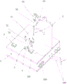
FIG. 1 is a block diagram of an embodiment of the present invention;
FIG. 2 is a block diagram of another perspective of an embodiment of the present invention;
FIG. 3 is a block diagram of another perspective of an embodiment of the present invention;
FIG. 4 is a block diagram of a test of an embodiment of the present invention.
Detailed Description
To further illustrate the various embodiments, the utility model provides the accompanying drawings. The accompanying drawings, which are incorporated in and constitute a part of this disclosure, illustrate embodiments of the utility model and, together with the description, serve to explain the principles of the embodiments. Those skilled in the art will appreciate still other possible embodiments and advantages of the present invention with reference to these figures. Elements in the figures are not drawn to scale and like reference numerals are generally used to indicate like elements.
The utility model will now be further described with reference to the accompanying drawings and detailed description.
As shown in fig. 1-4, a testing jig for a switching power supply comprises a base 1, a supporting frame 2, a lifting mechanism and a pressing mechanism, wherein a workbench 111 is arranged on the upper surface of the base 1, a limiting thimble 3 and a testing probe 4 which can elastically stretch up and down are arranged on the workbench 111, the limiting thimble 3 and the testing probe 4 are both arranged upwards, and the limiting thimble 3 is used for being propped against a limiting hole 51 of a PCB 5 of the switching power supply to be tested so as to limit the PCB 5.
In this embodiment, the base 1 is preferably a rectangular parallelepiped structure, so that the structure is more compact, but not limited thereto, and in other embodiments, the base 1 may also be a cube, a cylinder, etc., which can be easily implemented by those skilled in the art and will not be described in detail.
In this embodiment, the base 1 includes a lower case 12 and an upper cover 11, and the upper cover 11 is openably covered on the lower case 12 by a buckle 13, and the base 1 is configured to facilitate assembly and maintenance of internal circuits, but is not limited thereto.
In this embodiment, the lifting mechanism includes a lifting rod 61, a handle 63 and two transition pieces 62, the lifting rod 63 can be movably inserted into the supporting frame 2 up and down, the handle 63 is substantially L-shaped, the outer end of the handle 63 is hinged to the supporting frame 2, the first end of the two transition pieces 62 is hinged to two sides of the turning of the handle 63, the second end of the two transition pieces is hinged to two sides of the upper end of the lifting rod 61, the pressing mechanism is fixed at the lower end of the lifting rod 61, and the lifting rod 61 can be driven to lift by rotating the handle 63, so as to drive the pressing mechanism to lift and switch between a lifting position and a lowering position. The lifting mechanism has the advantages of simple structure, easy realization, low cost and simple and convenient operation, and in other embodiments, the lifting mechanism can also be realized by other existing lifting mechanisms, such as a lifting mechanism driven by a cylinder.
In this embodiment, the pressing mechanism includes a fixing plate 71 and a first push rod 72, the fixing plate 71 is fixed at the lower end of the lifting rod 61, the top end of the first push rod 72 is fixed at the lower surface of the fixing plate 61, and the lower end of the first push rod 72 is used for pressing against the upper surface of the PCB 5. The pressing mechanism is simple in structure, easy to realize and low in cost, but is not limited to the structure.
Preferably, in this embodiment, the number of the first lift pins 72 is 4, and the first lift pins correspond to four corners of the PCB 5, so that the pressure applied to the PCB 5 is more uniform, and the PCB 5 can descend in parallel, but not limited thereto.
Further, in this embodiment, the fixing plate 71 is further provided with a guide hole, and correspondingly, the upper surface of the base 1 is provided with a guide post 8 penetrating through the guide hole, so that the guide cooperation between the guide post 8 and the guide hole improves the up-and-down moving stability of the fixing plate 71.
Preferably, the number of the guide holes is 2, and the guide holes are respectively arranged on two sides of the fixing portion 71, and correspondingly, the number of the guide posts 8 is also two, and of course, in other embodiments, the number of the guide holes and the number of the guide posts 8 may also be 1 or more than 2.
In this embodiment, the test probe 4 is preferably a spring probe, which is simple in structure and easy to implement. The number and the position of the test probes 4 can be set according to the condition of the test points of the PCB board 5 to be tested, which can be easily implemented by those skilled in the art and will not be described in detail.
In this embodiment, the number of the position-limiting ejector pins 3 is 4, and the number of the position-limiting ejector pins 3 corresponds to four corners of the PCB 5, respectively, so that the positioning accuracy and the stability of supporting the PCB 5 are improved, but not limited thereto, and in other embodiments, the number of the position-limiting ejector pins 3 may be less than 4 or more than 4.
Furthermore, in this embodiment, the top of the limiting thimble 3 is a conical structure, the size of the bottom of the conical structure is larger than the size of the limiting hole 51 of the PCB 5, and the height of the bottom of the conical structure is higher than the top of the test probe 4, so that when the PCB 5 is limited on the limiting thimble 3 and the pressing mechanism is not pressed down, the PCB 5 is higher than the top of the test probe 4 and does not contact the test probe 4, thereby avoiding touching the test probe 4 when the PCB 5 is taken and placed, causing scratch or electric shock, and the like, and improving the safety.
In this embodiment, the limiting ejector pin 3 can be implemented by a spring ejector pin, and is simple in structure and easy to implement, but not limited thereto.
In this embodiment, the upper surface of the base 1 is further provided with a power switch 9, and the input power is connected to the corresponding test probe 4 through the power switch 9, so as to supply power to the PCB 5. Of course, in other embodiments, the power switch 9 can be disposed at other positions of the base 1, such as the front side, etc., which can be easily realized by those skilled in the art and will not be described in detail.
In this embodiment, the power switch 9 is implemented by a ship-type switch, such as a ship-type switch model PA66, with an indicator light, and the safety is high, but not limited thereto.
Furthermore, in this embodiment, the safety protection device further includes a travel switch 100, the travel switch 100 is connected in series to the output end of the power switch 9, the travel switch 100 is disposed on the upper surface of the base 1, the second push rod 73 is disposed on the fixing plate 71, when the fixing plate 71 is located at the descending position, the second push rod 73 pushes down the travel switch 100 to trigger the travel switch 100 to be conducted, at this time, the test probe 4 connected to the power switch 9 has an electrical output, and it is avoided that when no test is performed, the test probe 4 connected to the power switch 9 has an electrical output to cause a test person to get an electric shock by mistake, thereby further improving the safety.
In this embodiment, the rear side of the base 1 is provided with a wiring portion 200, and the corresponding test probes 4 are respectively connected to the wiring portion 200 through wires and then connected to a test instrument (not shown in the figure) through the wiring portion 200, so that the wiring is simpler and more convenient. The test instrument can comprise one or more of an electronic load instrument, a voltmeter, an oscilloscope and the like and is used for detecting the output voltage, the current, the power, the ripple and the like of the switching power supply.
In this embodiment, an ac power socket 300 is disposed on the rear side of the base 1 for receiving ac power, and the ac power socket 300 is connected to the power switch 9 through a wire.
In this embodiment, the connecting wire of each part all sets up in base 1 for the circuit is succinct, easily realizes, and the security is high, and wholly more pleasing to the eye.
The testing process comprises the following steps:
according to the performance to be tested, the testing jig of the switching power supply is connected with corresponding testing equipment through a wiring part 200, then a limiting hole 51 of a PCB 5 of the switching power supply to be tested is arranged on a limiting thimble 3 in a penetrating mode for positioning, a power switch 9 is turned on, a handle 63 is rotated, a driving fixing plate 71 is lowered to a descending position, a first ejector rod 72 presses down the PCB 5 to enable a testing point of the PCB 5 to be tightly pressed on a testing probe 4, meanwhile, a second ejector rod 73 presses down a travel switch 100 to trigger the travel switch 100 to be conducted, as shown in figure 4, the switching power supply to be tested is powered on, the testing equipment can carry out related performance testing, after the testing is completed, the handle 63 is rotated to drive the fixing plate 71 to be lifted to a lifting position, as shown in figure 1, the first ejector rod 72 is separated from the PCB 5, the PCB 5 is lifted under the restoring force of the limiting thimble 3 to be separated from the testing probe 4, and then the PCB 5 is taken out, the limiting hole 51 of the PCB 5 of the next switching power supply to be tested is arranged on the limiting thimble 3 in a penetrating mode for positioning, then testing is carried out according to the steps, and the circuit is circulated, so that when the PCB 5 of the switching power supply to be tested is replaced, rewiring is not needed, operation is simple and convenient, testing working hours are reduced, testing efficiency is improved, testing cost is reduced, frequent wiring is avoided, the problem of poor wiring is solved, and testing accuracy is improved.
While the utility model has been particularly shown and described with reference to a preferred embodiment, it will be understood by those skilled in the art that various changes in form and detail may be made therein without departing from the spirit and scope of the utility model as defined by the appended claims.
Claims (10)
1. The utility model provides a switching power supply's test fixture which characterized in that: the on-line screen storage device comprises a base, the support frame, elevating system and pushing mechanism, the upper surface of base is equipped with the workstation, be equipped with elastic expansion's spacing thimble and test probe on the workstation, spacing thimble and test probe all set up, spacing thimble is used for the top to carry on spacingly in the spacing downthehole of the PCB board of switching power supply that awaits measuring, the support frame sets up the upper surface at the base, elevating system sets up on the support frame, be used for the drive to push down the mechanism and go up and down to switch between rising position and decline position, when pushing down the mechanism and being in the decline position, the test point that pushes down the PCB board and make the PCB board presses on test probe's top and the electricity is connected.
2. The testing fixture of the switching power supply according to claim 1, wherein: the lifting mechanism comprises a lifting rod, a handle and two transition pieces, the lifting rod can be movably arranged on the support frame in a penetrating mode from top to bottom, the handle is hinged to the support frame, the first end of each transition piece is hinged to the handle, the second end of each transition piece is hinged to the upper end of the lifting rod, the pressing mechanism is fixed to the lower end of the lifting rod, the lifting rod can be driven to lift by rotating the handle, and therefore the pressing mechanism is driven to lift and switch between a lifting position and a descending position.
3. The testing fixture of the switching power supply according to claim 2, wherein: the pressing mechanism comprises a fixing plate and a first ejector rod, the fixing plate is fixed at the lower end of the lifting rod, the top end of the first ejector rod is fixed at the lower surface of the fixing plate, and the lower end of the first ejector rod is used for abutting against the upper surface of the PCB.
4. The testing fixture of the switch power supply of claim 3, wherein: the quantity of first ejector pin is 4, corresponds to four angles of PCB board respectively.
5. The testing fixture of the switch power supply of claim 3, wherein: the fixed plate is also provided with a guide hole, and correspondingly, the upper surface of the base is provided with a guide post penetrating through the guide hole.
6. The testing fixture of the switch power supply of claim 5, wherein: the number of the guide holes is 2, and correspondingly, the number of the guide columns is 2.
7. The testing fixture of the switching power supply according to claim 1, wherein: the top of the limiting thimble is of a conical structure, the size of the bottom of the conical structure is larger than that of the limiting hole of the PCB, and the height of the bottom of the conical structure is higher than that of the top of the testing probe.
8. The testing fixture of the switching power supply according to claim 1, wherein: and the base is also provided with a power switch, and an input power supply is connected with the corresponding test probe through the power switch.
9. The testing fixture of the switching power supply according to claim 8, wherein: the power supply device is characterized by further comprising a travel switch, the travel switch is connected to the output end of the power supply switch in series, the travel switch is arranged on the upper surface of the base, the pressing mechanism is further provided with a second ejector rod, and when the pressing mechanism is located at a descending position, the second ejector rod presses the travel switch to trigger the travel switch to be conducted.
10. The testing fixture of the switching power supply according to claim 1, wherein: the rear side of the base is provided with a wiring part, and the test probe is connected with a corresponding test instrument through the wiring part.
Priority Applications (1)
| Application Number | Priority Date | Filing Date | Title |
|---|---|---|---|
| CN202121550770.5U CN215494029U (en) | 2021-07-08 | 2021-07-08 | Testing jig for switching power supply |
Applications Claiming Priority (1)
| Application Number | Priority Date | Filing Date | Title |
|---|---|---|---|
| CN202121550770.5U CN215494029U (en) | 2021-07-08 | 2021-07-08 | Testing jig for switching power supply |
Publications (1)
| Publication Number | Publication Date |
|---|---|
| CN215494029U true CN215494029U (en) | 2022-01-11 |
Family
ID=79725381
Family Applications (1)
| Application Number | Title | Priority Date | Filing Date |
|---|---|---|---|
| CN202121550770.5U Active CN215494029U (en) | 2021-07-08 | 2021-07-08 | Testing jig for switching power supply |
Country Status (1)
| Country | Link |
|---|---|
| CN (1) | CN215494029U (en) |
-
2021
- 2021-07-08 CN CN202121550770.5U patent/CN215494029U/en active Active
Similar Documents
| Publication | Publication Date | Title |
|---|---|---|
| CN201569724U (en) | Test tool structure for PCBA product joined board | |
| CN209471222U (en) | Automate lithium battery group detection device | |
| CN211236174U (en) | Testing tool for switching power supply | |
| CN203117290U (en) | Resistance test tool | |
| CN209992543U (en) | Circuit board testing jig | |
| CN215494029U (en) | Testing jig for switching power supply | |
| CN205427081U (en) | VCXO crystal electrical performance test mechanism | |
| CN217981735U (en) | PCB power consumption test tool | |
| CN216350802U (en) | PCBA test jig | |
| CN212905259U (en) | Insulation test fixture for semiconductor power device | |
| CN213023232U (en) | Finished product electrical property test jig | |
| CN114696744A (en) | Solar cell test equipment | |
| CN215493975U (en) | Circuit board test fixture | |
| CN212410810U (en) | Test tool for DC/DC power module | |
| CN207910863U (en) | A kind of antenna for mobile phone test device | |
| CN220120939U (en) | Multifunctional testing device and multifunctional testing system | |
| CN220626588U (en) | Automatic detection structure of PCB circuit board | |
| CN111025126A (en) | Automatic test equipment for bare board of controller circuit board | |
| CN212160034U (en) | Test fixture for testing internal electrical parameters of power supply | |
| CN219978474U (en) | Relay test bench | |
| CN219751213U (en) | Chip double-module material taking and discharging device | |
| CN219777734U (en) | Clamping tool for testing PCB contacts and keys | |
| CN116068372A (en) | Multifunctional testing tool suitable for three-in-one television main board | |
| CN220357205U (en) | Switch use number of times testing arrangement | |
| CN216209332U (en) | Quick detection device of photovoltaic LED lighting control integrated board |
Legal Events
| Date | Code | Title | Description |
|---|---|---|---|
| GR01 | Patent grant | ||
| GR01 | Patent grant |