Little band delay line based on defect ground structure
Technical field
The utility model relates to a kind of delay-line structure, relates in particular to a kind of little band delay line based on defect ground structure.
Background technology
Delay line is widely used in phased array radar, satellite communication and the various high precision measurement instrument, and these systems all can change parameters such as phase place, distance through the accurate control to time of delay, thereby realizes systemic-function.Little band delay line has characteristics such as the frequency band coverage is wide, size is little, loss is little, dispersion characteristics are weak, economic and reliable, in the short delay system of high frequency, has incomparable performance and advantage.
Strip line is because its distinctive non-mode dispersion characteristics, is even more important in the system that group delay fluctuation etc. is had relatively high expectations.Yet the mode that realizes strip line at present is owing to reasons such as technologies, fully the non-mode dispersion characteristics on the realization theory.The mode that substitutes its structure has a lot, such as the mode of two little band plates stacks, constitutes strip line with the method for screw or other physical fixation, and the shortcoming that this mode exists has: be prone to slit between the generation plate, cause electric property uncontrollable; Can't add other functional circuits, realize complicated monolithic strip line system etc.The mode of using the no copper base covering of adding identical dielectric constant on the microstrip line is also arranged, and there is above-mentioned shortcoming equally in this mode, and is not easy to processing and practical implementation.
The notion of defect ground structure (DGS) is proposed in 2000 by C.S.Kim etc., and this structure and electro-magnetic bandgap (DCS) similar also is through etched figure is achieved in the ground of microstrip line; Common etched figure has dumbbell shape, spirality and H shape; Compare with EBG, the etching element number equivalent electric circuit few, the unit that DCS adopts is easy to extract, thereby in design; Need not consider array factors such as unit interval, simple.But at present, also do not see the relevant report that this kind defect ground structure is applied to little band delay line field.
Summary of the invention
In view of this, the purpose of the utility model provides a kind of little band delay line based on defect ground structure, and the little band delay line than routine has the advantage that size is little, Insertion Loss is little, precision is high, reliability is high.
The purpose of the utility model realizes through following technical scheme:
Should comprise based on little band delay line of defect ground structure
Little band delay-line structure; Comprise dielectric-slab; The front of said dielectric-slab is left hand delay line or right-hand man's composite construction delay line of arbitrary structures; The back side of said dielectric-slab is the metal covering that has removed the part body, and the part of removing and the front delay line defect ground structure that constitutes that is complementary is equivalent to shunt inductance;
Radio-frequency joint is arranged at little band delay line both sides, and is electrically connected with little band delay-line structure.
Further, also comprise housing, this housing is the cuboid metal shell of indent, is used to seal whole little band delay line, and said radio-frequency joint is installed on the housing;
Further, said little band delay-line structure is fixed and back side good earth through non-metallic screw hole;
Further, all exposed metals all adopt gold-plated processing on said little band delay-line structure;
Further, the thickness thickness of the metal covering of said little band delay-line structure is 0.035-0.08mm;
Further, said little band delay-line structure uses conducting resinl to be fixed on the dielectric-slab.
The beneficial effect of the utility model is:
Traditional little band delay line is because problems such as technology, precision; Cause being difficult to be applicable to the required precision higher system; Such as highly sophisticated device and Large Phased Array Radar etc.; The utility model has made full use of the low Insertion Loss characteristic of high time delay of left hand delay line or right-hand man's composite delay line through adopting the little band delay-line structure based on defective ground and left hand delay line, and the characteristic of the easy realization of defect ground structure, easy tuning and easy processing; Little band delay line than routine has the advantage that size is little, Insertion Loss is little, precision is high, reliability is high.
Other advantages, target and the characteristic of the utility model will be set forth in specification subsequently to a certain extent; And to a certain extent; Based on being conspicuous to those skilled in the art, perhaps can from the practice of the utility model, obtain instruction to investigating of hereinafter.The target of the utility model and other advantages can realize and obtain through following specification.
Description of drawings
For the purpose, technical scheme and the advantage that make the utility model is clearer, will combine accompanying drawing that the utility model is done further to describe in detail below, wherein:
Fig. 1 is defective ground left hand delay-line structure figure;
Fig. 2 is the structural representation of little band delay-line structure;
Fig. 3 be utility model the assembling sketch map.
Embodiment
Below will be with reference to accompanying drawing, the preferred embodiment of the utility model is carried out detailed description.Should be appreciated that preferred embodiment has been merely explanation the utility model, rather than in order to limit the protection range of the utility model.
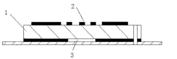
As shown in the figure, comprise little band delay-line structure 7 and radio-frequency joint based on little band delay line of defect ground structure; Wherein little band delay-line structure 7 comprises dielectric-slab 1; The front of dielectric-slab is left hand delay line or right-hand man's composite construction delay line 2; The back side of dielectric-slab 1 is the metal covering that has removed the part body, and the part of removing and the front delay line defect ground structure 3 that constitutes that is complementary is equivalent to shunt inductance; In the practice process, dielectric-slab can adopt some sheet materials of in the circuit board making field, using always at present.
Radio-frequency joint is arranged at the both sides of little band delay-line structure, and is electrically connected with little band delay-line structure.
For the ease of installing and delay-line structure being played a protective role; The utility model also comprises a housing 5; This housing 5 is the cuboid metal shell of indent, is used to seal the circuit board of whole little band delay-line structure 7, and radio-frequency joint is installed on the radio-frequency joint installation position 6 of housing 5.
In the present embodiment, the inner-cavity structure of shell should closely cooperate with little band delay-line structure and not have obvious slit; The radio-frequency joint that uses is the microstrip line joint, and interior pin is a flat; Electrode is revealed in the blind groove of the little band plate of monolithic multilayer place, and with shell on the interior pin of radio-frequency joint closely cooperate, do not have obvious spacing; The upper surface of the little band plate of multilayer and the spacing of cover inner surface should satisfy the electromagnetic compatibility effect.
As further improvement, little band delay-line structure is fixed and back side good earth through non-metallic screw 4, and all exposed metals all adopt gold-plated processing on little band delay-line structure, and the thickness of the metal covering of little band delay line is 0.035mm.The position of non-metallic screw hole 4 need be satisfied: do not intersect with the intermediate retardation line circuit, and leave a determining deviation, a plurality of screw holes need and circuit board center symmetric arrays.
As further improvement, said little band delay line uses conducting resinl to be fixed on the dielectric-slab 1, and in the present embodiment, dielectric-slab 1 adopts a rogers5880 metal medium plate.Should prevent that conducting resinl is spilled in the defective ground in the position on defective ground when bonding.
Delay line need use Electromagnetic Simulation softwares such as IE3D or ADS to obtain optimal result, and single delay line adopts conventional right-hand man to meet transmission line structure, with the realization of better fit defect ground structure.
Explanation is at last; Above embodiment is only unrestricted in order to the technical scheme of explanation the utility model; Although with reference to preferred embodiment the utility model is specified, those of ordinary skill in the art should be appreciated that and can make amendment or be equal to replacement the technical scheme of the utility model; And not breaking away from the aim and the scope of present technique scheme, it all should be encompassed in the middle of the claim scope of the utility model.