CN1465037A - Matrix type display apparatus - Google Patents
Matrix type display apparatus Download PDFInfo
- Publication number
- CN1465037A CN1465037A CN02802614A CN02802614A CN1465037A CN 1465037 A CN1465037 A CN 1465037A CN 02802614 A CN02802614 A CN 02802614A CN 02802614 A CN02802614 A CN 02802614A CN 1465037 A CN1465037 A CN 1465037A
- Authority
- CN
- China
- Prior art keywords
- circuit
- lines
- type surface
- sets
- sweep trace
- Prior art date
- Legal status (The legal status is an assumption and is not a legal conclusion. Google has not performed a legal analysis and makes no representation as to the accuracy of the status listed.)
- Pending
Links
- 239000011159 matrix material Substances 0.000 title claims abstract description 58
- 239000000758 substrate Substances 0.000 claims description 94
- 239000000463 material Substances 0.000 claims description 53
- 230000005284 excitation Effects 0.000 claims description 15
- 238000010894 electron beam technology Methods 0.000 claims description 14
- 230000005670 electromagnetic radiation Effects 0.000 claims description 8
- 238000007650 screen-printing Methods 0.000 claims description 5
- 230000005684 electric field Effects 0.000 claims description 4
- 239000012780 transparent material Substances 0.000 claims description 4
- 238000007599 discharging Methods 0.000 claims description 2
- 239000002184 metal Substances 0.000 claims 6
- 239000011888 foil Substances 0.000 claims 2
- 239000010410 layer Substances 0.000 description 23
- 239000010408 film Substances 0.000 description 16
- 230000014509 gene expression Effects 0.000 description 15
- 239000011521 glass Substances 0.000 description 13
- RYGMFSIKBFXOCR-UHFFFAOYSA-N Copper Chemical compound [Cu] RYGMFSIKBFXOCR-UHFFFAOYSA-N 0.000 description 11
- 239000004020 conductor Substances 0.000 description 11
- 229910052802 copper Inorganic materials 0.000 description 11
- 239000010949 copper Substances 0.000 description 11
- 238000000034 method Methods 0.000 description 9
- PXHVJJICTQNCMI-UHFFFAOYSA-N Nickel Chemical compound [Ni] PXHVJJICTQNCMI-UHFFFAOYSA-N 0.000 description 8
- 230000005855 radiation Effects 0.000 description 8
- 239000010409 thin film Substances 0.000 description 8
- 229920006254 polymer film Polymers 0.000 description 7
- 230000003446 memory effect Effects 0.000 description 6
- 239000003989 dielectric material Substances 0.000 description 5
- VYZAMTAEIAYCRO-UHFFFAOYSA-N Chromium Chemical compound [Cr] VYZAMTAEIAYCRO-UHFFFAOYSA-N 0.000 description 4
- 230000008901 benefit Effects 0.000 description 4
- 229910052804 chromium Inorganic materials 0.000 description 4
- 239000011651 chromium Substances 0.000 description 4
- 238000005401 electroluminescence Methods 0.000 description 4
- 238000012423 maintenance Methods 0.000 description 4
- 229910052759 nickel Inorganic materials 0.000 description 4
- 238000004544 sputter deposition Methods 0.000 description 4
- 230000002146 bilateral effect Effects 0.000 description 3
- 230000008859 change Effects 0.000 description 3
- 230000008878 coupling Effects 0.000 description 3
- 238000010168 coupling process Methods 0.000 description 3
- 238000005859 coupling reaction Methods 0.000 description 3
- 238000005516 engineering process Methods 0.000 description 3
- 238000005530 etching Methods 0.000 description 3
- 238000004519 manufacturing process Methods 0.000 description 3
- 238000007639 printing Methods 0.000 description 3
- 230000000007 visual effect Effects 0.000 description 3
- OKTJSMMVPCPJKN-UHFFFAOYSA-N Carbon Chemical compound [C] OKTJSMMVPCPJKN-UHFFFAOYSA-N 0.000 description 2
- 102000029749 Microtubule Human genes 0.000 description 2
- 108091022875 Microtubule Proteins 0.000 description 2
- ATJFFYVFTNAWJD-UHFFFAOYSA-N Tin Chemical compound [Sn] ATJFFYVFTNAWJD-UHFFFAOYSA-N 0.000 description 2
- 230000015572 biosynthetic process Effects 0.000 description 2
- 229910052799 carbon Inorganic materials 0.000 description 2
- 238000002474 experimental method Methods 0.000 description 2
- 238000009413 insulation Methods 0.000 description 2
- 239000011229 interlayer Substances 0.000 description 2
- 238000004020 luminiscence type Methods 0.000 description 2
- 238000005259 measurement Methods 0.000 description 2
- 230000006386 memory function Effects 0.000 description 2
- 210000004688 microtubule Anatomy 0.000 description 2
- 239000011368 organic material Substances 0.000 description 2
- 229920002120 photoresistant polymer Polymers 0.000 description 2
- 229910004205 SiNX Inorganic materials 0.000 description 1
- 239000004411 aluminium Substances 0.000 description 1
- XAGFODPZIPBFFR-UHFFFAOYSA-N aluminium Chemical compound [Al] XAGFODPZIPBFFR-UHFFFAOYSA-N 0.000 description 1
- 229910052782 aluminium Inorganic materials 0.000 description 1
- 230000005540 biological transmission Effects 0.000 description 1
- 239000003990 capacitor Substances 0.000 description 1
- 239000002800 charge carrier Substances 0.000 description 1
- 239000011248 coating agent Substances 0.000 description 1
- 238000000576 coating method Methods 0.000 description 1
- 239000012141 concentrate Substances 0.000 description 1
- 238000010276 construction Methods 0.000 description 1
- 239000006071 cream Substances 0.000 description 1
- 238000010586 diagram Methods 0.000 description 1
- 238000009826 distribution Methods 0.000 description 1
- 230000000694 effects Effects 0.000 description 1
- 239000003292 glue Substances 0.000 description 1
- 238000010438 heat treatment Methods 0.000 description 1
- 238000002347 injection Methods 0.000 description 1
- 239000007924 injection Substances 0.000 description 1
- 238000003475 lamination Methods 0.000 description 1
- 230000007246 mechanism Effects 0.000 description 1
- 239000012528 membrane Substances 0.000 description 1
- 150000004767 nitrides Chemical class 0.000 description 1
- NJPPVKZQTLUDBO-UHFFFAOYSA-N novaluron Chemical compound C1=C(Cl)C(OC(F)(F)C(OC(F)(F)F)F)=CC=C1NC(=O)NC(=O)C1=C(F)C=CC=C1F NJPPVKZQTLUDBO-UHFFFAOYSA-N 0.000 description 1
- 230000003287 optical effect Effects 0.000 description 1
- 239000002245 particle Substances 0.000 description 1
- 238000000059 patterning Methods 0.000 description 1
- 230000002093 peripheral effect Effects 0.000 description 1
- 229920000642 polymer Polymers 0.000 description 1
- 230000002265 prevention Effects 0.000 description 1
- 230000008569 process Effects 0.000 description 1
- 238000007634 remodeling Methods 0.000 description 1
- 238000012827 research and development Methods 0.000 description 1
- 230000004044 response Effects 0.000 description 1
- 238000007789 sealing Methods 0.000 description 1
- 230000035939 shock Effects 0.000 description 1
- 229910052709 silver Inorganic materials 0.000 description 1
- 239000004332 silver Substances 0.000 description 1
- 230000001052 transient effect Effects 0.000 description 1
Images


Classifications
-
- G—PHYSICS
- G09—EDUCATION; CRYPTOGRAPHY; DISPLAY; ADVERTISING; SEALS
- G09G—ARRANGEMENTS OR CIRCUITS FOR CONTROL OF INDICATING DEVICES USING STATIC MEANS TO PRESENT VARIABLE INFORMATION
- G09G3/00—Control arrangements or circuits, of interest only in connection with visual indicators other than cathode-ray tubes
- G09G3/20—Control arrangements or circuits, of interest only in connection with visual indicators other than cathode-ray tubes for presentation of an assembly of a number of characters, e.g. a page, by composing the assembly by combination of individual elements arranged in a matrix no fixed position being assigned to or needed to be assigned to the individual characters or partial characters
-
- G—PHYSICS
- G09—EDUCATION; CRYPTOGRAPHY; DISPLAY; ADVERTISING; SEALS
- G09F—DISPLAYING; ADVERTISING; SIGNS; LABELS OR NAME-PLATES; SEALS
- G09F9/00—Indicating arrangements for variable information in which the information is built-up on a support by selection or combination of individual elements
- G09F9/30—Indicating arrangements for variable information in which the information is built-up on a support by selection or combination of individual elements in which the desired character or characters are formed by combining individual elements
-
- H—ELECTRICITY
- H01—ELECTRIC ELEMENTS
- H01J—ELECTRIC DISCHARGE TUBES OR DISCHARGE LAMPS
- H01J31/00—Cathode ray tubes; Electron beam tubes
- H01J31/08—Cathode ray tubes; Electron beam tubes having a screen on or from which an image or pattern is formed, picked up, converted, or stored
- H01J31/10—Image or pattern display tubes, i.e. having electrical input and optical output; Flying-spot tubes for scanning purposes
- H01J31/12—Image or pattern display tubes, i.e. having electrical input and optical output; Flying-spot tubes for scanning purposes with luminescent screen
- H01J31/123—Flat display tubes
- H01J31/125—Flat display tubes provided with control means permitting the electron beam to reach selected parts of the screen, e.g. digital selection
- H01J31/127—Flat display tubes provided with control means permitting the electron beam to reach selected parts of the screen, e.g. digital selection using large area or array sources, i.e. essentially a source for each pixel group
-
- H—ELECTRICITY
- H10—SEMICONDUCTOR DEVICES; ELECTRIC SOLID-STATE DEVICES NOT OTHERWISE PROVIDED FOR
- H10K—ORGANIC ELECTRIC SOLID-STATE DEVICES
- H10K59/00—Integrated devices, or assemblies of multiple devices, comprising at least one organic light-emitting element covered by group H10K50/00
- H10K59/10—OLED displays
- H10K59/17—Passive-matrix OLED displays
- H10K59/179—Interconnections, e.g. wiring lines or terminals
-
- G—PHYSICS
- G09—EDUCATION; CRYPTOGRAPHY; DISPLAY; ADVERTISING; SEALS
- G09G—ARRANGEMENTS OR CIRCUITS FOR CONTROL OF INDICATING DEVICES USING STATIC MEANS TO PRESENT VARIABLE INFORMATION
- G09G2300/00—Aspects of the constitution of display devices
- G09G2300/04—Structural and physical details of display devices
- G09G2300/0421—Structural details of the set of electrodes
- G09G2300/0426—Layout of electrodes and connections
-
- G—PHYSICS
- G09—EDUCATION; CRYPTOGRAPHY; DISPLAY; ADVERTISING; SEALS
- G09G—ARRANGEMENTS OR CIRCUITS FOR CONTROL OF INDICATING DEVICES USING STATIC MEANS TO PRESENT VARIABLE INFORMATION
- G09G2320/00—Control of display operating conditions
- G09G2320/02—Improving the quality of display appearance
- G09G2320/0223—Compensation for problems related to R-C delay and attenuation in electrodes of matrix panels, e.g. in gate electrodes or on-substrate video signal electrodes
-
- H—ELECTRICITY
- H10—SEMICONDUCTOR DEVICES; ELECTRIC SOLID-STATE DEVICES NOT OTHERWISE PROVIDED FOR
- H10K—ORGANIC ELECTRIC SOLID-STATE DEVICES
- H10K59/00—Integrated devices, or assemblies of multiple devices, comprising at least one organic light-emitting element covered by group H10K50/00
- H10K59/80—Constructional details
- H10K59/87—Passivation; Containers; Encapsulations
Landscapes
- Engineering & Computer Science (AREA)
- Physics & Mathematics (AREA)
- General Physics & Mathematics (AREA)
- Theoretical Computer Science (AREA)
- Computer Hardware Design (AREA)
- Cathode-Ray Tubes And Fluorescent Screens For Display (AREA)
- Devices For Indicating Variable Information By Combining Individual Elements (AREA)
- Control Of Indicators Other Than Cathode Ray Tubes (AREA)
- Gas-Filled Discharge Tubes (AREA)
Abstract
A matrix type display apparatus includes a display panel (11, 27) having a first main surface where a display image is displayed and a second main surface which is approximately parallel to the first main surface, scan lines (12) parallel to one another and arranged on the display panel, signal lines (14) parallel to one another and intersecting the scan lines, display pixels (17) provided at the intersecting points between the scan lines and the signal lines, and a rear surface wiring (23) formed on the second main surface and connected at least to the scan lines or the signal lines at the opposing end portion of the display panel.
Description
Technical field
The present invention relates to matrix display, for example, use the electron-beam excitation luminescent material display of plane electronics power supply (SCE transmitter), plasma display panel, or utilize the electroluminescent display of the electro optical phenomenon of luminescent material, particularly have the matrix display of improved wire structures.
Background technology
Display mode with the electron beam excitation light-emitting material has been widely used in the televisor that uses cathode-ray tube (CRT), and it is the high quality image video equipment.This is because this display mode has high response speed and wide visual angle, can be used to the light emitting-type display device.
But, along with the change of screen size is big, the weight and the degree of depth of cathode-ray tube (CRT) also increase, and the cathode-ray tube (CRT) of prior art, 40-inch are limit.Therefore, 30 inches or littler cathode-ray tube (CRT) are generally for household use.On the other hand, the picture intelligence of NTSC type has been transformed into high eye-minded signal, and requires to realize in high quality large screen display.
In view of the above, various matrix type thin plate displays are studied and develop, the practical application that wherein has.
As up-to-date giant-screen thin display, have use the plane electronics source (E.Yamaguchi, et.al., " A10-in.SCE-emitter display ", Joumal of SID, Vol.5, p345,1997) electron-beam excitation luminescent material display.This electron-beam excitation luminescent material display has following advantage.That is, the electronic emission element that is arranged in the plane electronics power supply can be made with printing technology.This is the basis principle of luminosity identical with cathode-ray tube (CRT), launches because luminescent material is stimulated and only utilizes electronics.And then therefore the plane electronics power supply can, can use low withstand voltage driver IC with the driven that is higher than 10V.
As the field emission type electronic power supply, a kind of electronic power supply of so-called Spindt type is studied and develops, it is fined away the shape of electron emission part coning and realizes that the field is concentrated, the electronic power supply that utilizes the carbon microtubules that are about millimicron thickness in addition of research and development, and above-mentioned plane electronics power supply.Because an ejected electron is quickened with kilovolt high pressure of level, luminescent material is excited, and causes the light emission, and the characteristics of this electronic power supply are to obtain the high-quality identical with cathode-ray tube (CRT).
Another example of large screen display is, plasma display panel (PDP), and it forms wiring according to the printing mode or pixel is realized giant-screen plate cheaply, has entered practical application.Owing to the luminescent material that this PDP utilizes the ultraviolet ray of each pixel discharge generation that the plate surface is formed is luminous to obtain image, in theory, its displayed image is the similarly visual principle that produces of basis and cathode-ray tube (CRT).To be that luminescent material is subjected to ultraviolet ray excited with the difference of cathode-ray tube (CRT), and make its emission light by ultraviolet ray.Moreover gray scale shows generally to be controlled by discharge time, realizes by the pulse voltage that applies about 200V.
Also have, developed the electroluminescent matrix escope of electroluminescence (EL) phenomenon of utilizing luminescent material, be i.e. LED matrix display, its injection electronics and hole and the energy emission light that utilizes charge carrier to reconfigure.In a kind of mode in back, unimolecule or polymer organic material are used, and have redly, and the green and material blue streak emission characteristics forms in pixel, can panchromaticly show therefrom.
Fig. 1 is the basic structure of the matrix display of prior art.Sweep trace circuit 144 (144a, 144b ...) and signal wire circuit 145 (145a, 145b ...) be formed on the viewing area 141, pixel 146 is arranged on the point of crossing of these circuits.Sweep trace circuit 144 provides the controlling impulse voltage of a scan line drive circuit 142 to each pixel, and signal wire circuit 145 provides the shows signal voltage of a signal-line driving circuit 143 to each pixel.The structure of each pixel changes according to the display mode of display board.
Fig. 2 A and 2B are to use the planimetric map of electron-beam excitation luminescent material display board of field emission type flat electronic power supply and the viewgraph of cross-section of display board.Electrode 151 and 152 and conductive film 153 be formed on the insulating substrate 155, electron emission part 154 is formed on the part of these parts.Apply a voltage to electronic power supply from electrode 151 and 152, make electronics 159 enter vacuum from electron emission part 154 emissions.Ejected electron enters the anode electrode 156 that forms on the opposed glass substrate 158.
If enough height of anode voltage and anode electrode 156 are enough thin, electronics is by anode 156 and be injected into luminous material layer 157, makes luminescent material 157 luminous thus.Because the quantity of field emission electron can control according to the time that is applied to the voltage on electrode 151 and 152 or applies voltage, luminosity can be changed.
Fig. 3 is more detailed structural drawing.Electronic power supply 163 and sweep trace circuit 161 (161a, 161b ...) and signal wire circuit 162 (162a, 162b ...) connect.Pixel 165 is arranged on each point of crossing of sweep trace circuit 161 and signal wire circuit 162, and electronic power supply 163 is used for each pixel.The electronics emission of the electron emission part 164 of electronic power supply 163 is to control by the pulse voltage that is added on sweep trace circuit 161 and the signal wire circuit 162.
Fig. 4 is the virtual voltage pulse application method of the display board of this pattern.Reference character VA1, Va2, Va3 ... expression is added to the waveform of the voltage on the sweep trace circuit, corresponds respectively to the first, the second and the voltage waveform of three scan line circuit.Be added to after all sweep trace circuits finish in the pulse voltage of pulse width T and pulse voltage value-Vs, repeat to apply pulse since first sweep trace again.Reference character Vb1, Vb2, Vb3 represent to be added to the pulse voltage waveform of the shows signal of signal wire circuit, correspond respectively to the voltage waveform of the first, the second and the 3rd signal wire circuit.This pulse voltage and sweep trace pulse voltage apply synchronously, and its pulse width or voltage magnitude change according to brightness.In the present embodiment, brightness is controlled by pulse width.The magnitude of voltage that is added to the pulse voltage of signal wire circuit is that the difference of the magnitude of voltage of Vm and sweep trace circuit is added to the plane electronics power supply.The voltage of two kinds of level, that is, (0-(Vs))=Vs and (Vm-(Vs))=Vm+Vs be added to be added with-electronic power supply of the sweep trace circuit of Vs voltage on, promptly be added on the electronic power supply of selected sweep trace circuit.
By adjust Vs and Vm make electronic power supply in every kind of state can/can not discharge, electronics is launched from the electronic power supply of the selected sweep trace circuit that is added with voltage Vm, just launches light corresponding to the luminescent material of this pixel.Moreover the pulse width of the pulse voltage of signal wire circuit is depended in brightness, and Fig. 5 is the show state of the pixel that applies corresponding to the voltage that Fig. 4 describes.
Though described the electron-beam excitation luminescent material display board that uses the plane electronics power supply above, a current drive-type light-emitting diode display or a driving electroluminescent display also are the two ends display elements, they are connected with the signal wire circuit with the sweep trace circuit, and by the driving of the method shown in Fig. 3 to 5, though its structure is different with the structure of the basic pixel of Fig. 2 A and 2B description in theory.
The ultraviolet ray excited radiative Plasma Display of luminescent material that makes according to plasma discharge adopts the structure shown in Fig. 6.Driving pulse is added to sweep trace circuit 194 (194a, 194b from scan line drive circuit 191 ...), driving pulse is added to signal wire circuit 196 (196a, 196b from signal-line driving circuit 193 ...).
In plasma scope, once to discharge and finish by applying a potential pulse, discharge can not continue, and therefore necessary multiple discharge is with control brightness.After discharge for the first time, the continuous application pulse voltage makes brightness controlled by the discharge that memory effect keeps pulse number thus.The circuit that keeps this discharge is 195 (165a, 165b ...), voltage is by keeping pulse driving circuit 192 to provide.
In addition, use reset pulse and can eliminate memory effect.Pixel 197 is formed on sweep trace, on the point of crossing of signal wire and sustaining voltage circuit.It should be noted that dividing plate of number in the figure 198 expressions, in order to avoid discharge owing to the fault of adjacent image point.
Fig. 7 is a sectional view, the structure of a pixel parts of expression plasma scope.Sweep trace circuit 202 and maintenance impulse circuit 203 are formed on the glass substrate 201, and dielectric film etc. are formed on the lead, though do not illustrate.Signal wire circuit 206 is formed on the opposed substrate 205, and luminous material layer 207 is arranged in above it.
When an address pulse voltage is added on the sweep trace circuit 202, when the signal voltage pulse was added on the signal wire circuit 206, if the potential difference (PD) between two electrodes is enough high, discharge 208 will occur.Just after this, the sustaining voltage pulse alternately is added on the maintenance impulse circuit 203 continuously and is added on the sweep trace circuit 202, and reignition 208 thus.This is because stored charge remains on the deielectric-coating of electrode 202 and 203, and memory effect is provided.Use reset pulse and can eliminate stored charge and memory effect.Though brightness is determined that by discharge time because many times discharge generation is in the sweep time that limits, the width of each pulse is μ second or shorter time.
As mentioned above, though various matrix type display board has different principle of operation, in theory, by applying driving pulse voltage on mutually perpendicular sweep trace circuit and signal wire circuit, driving method can show arbitrary figure, comprises gray scale.This matrix type display board is developed/enters practical application, and it is a kind of approaching/light giant display, has replaced traditional cathode-ray tube (CRT), and cathode-ray tube (CRT) can not increase size because of the restriction of its degree of depth and weight.
In above-mentioned matrix type display board, drive signal is added on separately the pixel by sweep trace circuit and signal wire circuit.In the sweep trace circuit, because all pixels along the sweep trace circuit are targets of display operation when selecting pulse voltage to be applied in, therefore from the viewpoint of driving circuit, load is big especially.That is, in field emission type electron-beam excitation luminescent material display board or current drive-type LED display board, because big electric current flows into trace wiring, voltage is owing to conductor resistance descends.
On the other hand, in the electric field drive electroluminescent display board, owing to load capacitance and conductor resistance make the signal waveform distortion.Moreover, in plasma display panel, must being produced and be flowed owing to must apply the voltage and the discharge current of the pulse width of short time, this has also produced the problem that causes voltage drop owing to transient high-current just except voltage wave shape distortion.
The brightness that these problems have produced shown in Fig. 8 A is tilted.In plasma display panel, because the voltage tolerant of voltage drop discharge generation is different on the right of screen and the left side, the operation tolerance limit is little, makes to be difficult to increase size and to be difficult to realize high definition.
As a kind of method of avoiding this problem, the both sides that Fig. 8 B describes drive and can be considered.In this case, though brightness is reduced on the core of screen, the amount that reduces is compared light with monolateral driving, and the inclination of brightness becomes symmetry, has therefore improved the quality that shows greatly.
But, in mode shown in Fig. 8 B, it is two that driving circuit must become, and this has just increased cost.Further, a left side, the difference of minute differences in the right driving circuit timing or the voltage that applies all can cause the increase of power consumption or make driver LSI heating that this has also just influenced the performance of display board.
For example at Fig. 9 A, in driven electroluminescent display board shown in 9B and the 9C or the plasma display panel, electric current flows through a left side and right CMOS driving circuit in the cycle that left and right sides pulse departs from time each other, reactive power mainly consumes in the operation of only using charging current.
For example, Fig. 9 B represents such a case, and this mistiming of the gate voltage Vr of the cmos circuit on the right left both sides of plate and Vl is big, and electric current I w flows in respect to the time delay of Vr at Vl, and reactive power just was created in this cycle.What Fig. 9 C represented is that Vl is little with respect to the time delay of Vr.
Particularly, in plasma scope, a plurality of high-frequency impulses are applied in, and the heat that circuit produces is big, and overheated element also just produces.The deviation of the voltage of the IC that a right left side drives causes the generation of reactive power by driver LSI, if deviation is very big, substrate just makes the transistorized anti-state partially in the driving circuit change to forward bias condition, and this just causes that big electric current flows.
Therefore, require realization matrix type display board, it makes the brightness on the display screen even, reduces manufacturing cost and power consumption.
Summary of the invention
First purpose of the present invention provides a kind of matrix display, and it comprises:
A display board, it has first first type surface, and displayed image is shown on this surface, one second first type surface, it is parallel fully with first first type surface;
A plurality of sweep trace line arrangements are on display board and parallel to each other;
A plurality of signal wire circuits and a plurality of sweep trace circuits intersect arrangement, and the signal wire circuit is parallel to each other;
A plurality of display elements independent of each other, they are formed on each point of crossing of a plurality of sweep trace circuits and a plurality of signal wire circuits; With
A plurality of backs circuit is formed on second first type surface of display board and with a plurality of sweep trace circuits of the anti-end of display board and at least one of a plurality of signal wire circuits and links to each other.
Second purpose of the present invention be, a matrix type luminescent material display is provided, and it comprises:
One first substrate, it have one first first type surface and one fully with second first type surface of first major surfaces in parallel;
One second substrate, it is arranged in the opposite of first substrate in a vacuum with a predetermined gap, and the 3rd first type surface is arranged in the opposite of first first type surface, the 4th first type surface and the 3rd major surfaces in parallel, and manufacture by transparent material,
First substrate comprises:
A plurality of sweep trace circuits are arranged on first first type surface, and parallel to each other;
A plurality of signal wire circuits are arranged on first first type surface, and are on the direction of intersecting with a plurality of sweep trace circuits, parallel to each other;
A plurality of display elements independent of each other, they are formed on each point of crossing of a plurality of sweep trace circuits and a plurality of signal wire circuits, and are formed by the field emission type electronic power supply; With
A plurality of backs lead, they are arranged on second first type surface, and with the opposite ends of first substrate on a plurality of sweep trace circuits and at least one of a plurality of signal wire circuits be connected,
Second substrate comprises:
Anode, it is formed on the 3rd first type surface, in order to voltage to be provided,
The electron-beam excitation luminous material layer, it is formed on the 3rd first type surface.
Moreover the 3rd purpose of the present invention provides a matrix display, and it comprises:
A substrate, it has second first type surface of one first first type surface and and first major surfaces in parallel;
A plurality of sweep trace circuits that are arranged on first first type surface, they are parallel to each other;
The signal wire circuit that provides on a plurality of first first type surfaces, they intersect with a plurality of sweep trace circuits, and signal line is parallel to each other;
A plurality of display elements independent of each other, they are formed on each point of crossing of a plurality of sweep trace circuits and a plurality of signal wire circuits, and are made by the luminescent layer of electric current or electric field driven;
A plurality of back circuits that are arranged on second first type surface, they with the opposite ends of substrate on a plurality of sweep trace circuits and at least one of a plurality of signal wire circuits link to each other.
Moreover the 4th purpose of the present invention provides a kind of matrix type luminescent material display, and it comprises:
First substrate, it has second first type surface of first first type surface and and first major surfaces in parallel, and it is made by transparent material;
Second substrate, it is arranged in the opposite of first first type surface of first substrate with a predetermined gap in a vacuum, and the 3rd first type surface is arranged in the opposite of first first type surface, the 4th first type surface and the 3rd major surfaces in parallel,
First substrate comprises a plurality of sweep trace circuits, and they are arranged on first first type surface, and parallel to each other.
Second substrate comprises:
A plurality of signal wire circuits, they are arranged on the 3rd first type surface, and parallel to each other on the direction that a plurality of sweep trace circuits of first substrate intersect;
The ultraviolet excited light-emitting material layer, it is formed on the 3rd first type surface, and on the position corresponding with a plurality of display elements independent of each other, pixel is formed on each point of crossing of a plurality of sweep trace circuits and a plurality of signal wire circuits at least;
A plurality of back circuits that on the 4th surface, provide, they with the opposite ends of second substrate on a plurality of sweep trace circuits and at least one of a plurality of signal wire circuits link to each other.
Description of drawings
Fig. 1 is the structural drawing of traditional matrix display;
Fig. 2 A is the planimetric map of the electronic power supply on the pixel of display board, and Fig. 2 B is the sectional view of display board;
Fig. 3 is the further concrete structural drawing of Fig. 1;
Fig. 4 is the method for applied voltage pulse in electron-beam excitation type luminescent material display board;
Fig. 5 is the show state corresponding to the pixel of voltage application among Fig. 4;
Fig. 6 is the example of structure of plasma scope;
Fig. 7 is the single pixel structure of plasma display panel
Fig. 8 A and 8B are the states of the generation that brightness is tilted in the display;
Fig. 9 A, 9B, 9C explain the problem that occurs when driving circuit is arranged on the right of display board and the left side, wherein, Fig. 9 A is the circuit diagram of the output of driving circuit, Fig. 9 B is the state that reactive current takes place big time of the deviation when input voltage, and Fig. 9 C is the state of the deviation of input voltage little the time;
Figure 10 is a planimetric map, represents the simple structure of the matrix type display board of first embodiment;
Figure 11 is a cross sectional view, is illustrated in the display board that uses among first embodiment in the scan-line direction;
Figure 12 is a plan view, the complete structure of expression back circuit parts;
Figure 13 is a plan view, represents the back of whole plate.
Figure 14 is a planimetric map, represents the general structure of the matrix type display board of second embodiment;
Figure 15 A is a planimetric map, represents the driving pulse voltage among second embodiment, and Figure 15 B represents that luminosity distributes;
Figure 16 A is a type map to 16G, explains the estimation and the experimental technique of electromagnetic radiation noise of the display board of second embodiment;
Figure 17 A is a sectional view, represents the general structure of the matrix type display board of the 3rd embodiment, and Figure 17 B is the planimetric map of expression identical content;
Figure 18 A is a sectional view, represents the general structure of the matrix type display board of the 4th embodiment, and Figure 18 B amplifies, the sectional view of expression pixel region, and Figure 18 C is a planimetric map;
Figure 19 A is a sectional view, represents the general structure of the matrix type display board of the 5th embodiment, and Figure 19 B is a planimetric map:
Figure 20 is a planimetric map, represents the general structure of the matrix type display board of the 6th embodiment; With
Figure 21 is a sectional view, represents the general structure of the matrix type display board of the 6th embodiment.
Embodiment
In the embodiments of the invention that will describe, or sweep trace circuit or signal wire circuit, or both, all be connected with back side circuit on the back side of substrate on the both ends of substrate.Therefore, since the voltage drop that the conductor resistance of the sweep trace circuit that is connected with back side lead or signal wire circuit causes can be reduced.And then, apply a driving pulse to the sweep trace circuit by back side circuit, can solve the problem of the brightness inclination that causes by monolateral driving.Moreover, and on the both sides of sweep trace circuit, provide the structure of driving circuit to compare, can drive by single driving circuit, avoided increase cost and power consumption thus.
Embodiments of the invention will be described with reference to the accompanying drawings now.
First embodiment
Figure 10 to 13 is planimetric maps, the theory structure of the matrix display of the expression first embodiment of the present invention.
In Figure 10, sweep trace circuit 12 (12a, 12b, 12c ...) be formed on the horizontal direction of an insulating substrate (array substrate) 11, signal wire circuit 14 (14a, 14b, 14c ...) being formed on the vertical direction of insulating substrate (array substrate) 11, substrate 11 is made by glass substrate.Be used for the outside electrode tip 12A1 that connects, 12b1,12c1 ... 12a2,12b2,12c2 ... 14A1,14b1,14c1,, 14a2,14b2,14c2 is formed on the two ends of each circuit, and the quantity of sweep trace circuit is 480, the quantity of signal wire circuit is 640 * 3 (* 3 corresponding to pixel R, G and B), and wire pitch is 900 μ m and 300 μ m.
Pixel is formed on each point of crossing of sweep trace circuit 12 and signal wire circuit 14, and plane electronics power supply 17 plays the electronics radiated element, and it is arranged on each pixel.As a concrete structure of plane electronics power supply 17, one shown in Fig. 2 A and the 2B can be used, and the number of plane electronics power supply 17 is 480 at scan-line direction, is 640 * 3 in the signal wire direction.Sweep trace circuit 12 and signal wire circuit 14 are formed by Ag cream (Ag paste) by serigraphy.Moreover two kinds of link testers are crossed insulation course that printing forms and insulated from each other.
Should be noted that, the part of dotted line 16 expressions is seal areas among Figure 10, wherein electronic power supply 17 formation array substrate (back plate) 11 thereon is fixed on the opposed substrate (panel), luminous material layer and anode are arranged on panel, after completion, back plate and panel by the glaze glass capsulation be connected.Simultaneously, back plate and panel are sealed by several millimeters air gap.
Moreover, on the emission wavelength peak value, become red, green, blue fluorescent material and be used on the inside surface of panel, the pattern of panel formed with the back plate on the corresponding spacing of each pixel.That is, red emission, the number of the fluorescent material of each of green emission and blue streak emission is 640 in the signal wire direction in scan-line direction 480, spacing is 900 μ m.
The film-type aluminium lamination is formed on the luminous material layer, and the anode voltage Va of accelerated electron is applied in the display operation.After two plates of sealing, the inside of display element is evacuated by the gas outlet that is arranged in the outside, viewing area.The inside of the seal area of dotted line 16 expressions is regions of no pressure among Figure 10.
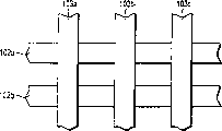
Figure 11 is the sectional view of the display board that uses in the present embodiment in scan-line direction, arranges to have sweep trace circuit 12, signal wire circuit on glass substrate 11, electronic power supply, and pad, pad is used to support delivery pipe and keeps two gaps between the substrate, though do not illustrate.In the panel side, luminous material layer and anode 28 are formed on the glass substrate 27, two substrates 11 and 27 in a vacuum sealed by seal area 29, and inboard 30 are evacuated by unshowned delivery pipe.
The said structure equipment with prior art basically is identical, but the back side circuit that improves the brightness inclination of screen also comprises in the present embodiment.That is, a plurality of back sides circuit 23 is formed on the back side of back plate 11, and the electrode tip 121 on the two ends of the sweep trace circuit 12 on these back side circuits 23 and the substrate both ends is connected with 122.
Drive IC 32 is arranged in the back side of back plate 11, and this drive IC 32 is connected with back side lead 23 by the band carrier 33 with conductive layer and anisotropic conductive film 31.Moreover driver IC 32 is connected with circuit board 34 by band carrier 33.And sweep trace circuit 12 is driven by drive IC 32.In this case, the driving pulse of drive IC 32 offers sweep trace circuit 12 by back side circuit 23, and sweep trace circuit 23 is driven by its two ends 121 and 122.
Figure 12 is a planimetric map, represents whole back side wire element.Desired back side circuit 23 is to form by the copper coin layer that forms on the polymer film is manufactured with etching technique through pattern.The conductor resistance of each back side circuit is 0.1ohm.In addition, the part of polymer film is eliminated, and this film is divided into 5 districts 24a, 24b, 24c, 24d, 24e and 24f.As shown in figure 11, these regional arrangements must be corresponding with the part that back plate lead electrode end 121 links to each other with 122, corresponding with the side surface portion of back plate, corresponding with the back of the body surface portion of back plate, they play the support effect, prevent that electrical short appears in back side circuit in assembling process, or owing to mechanical shock disconnects.
Drive IC 32 is arranged in the gap of Ranvier's membrane 24c and 24d and is connected as shown in figure 11.The copper conductor that it should be noted that the coupling part preferably is stamped anticorrosion conducting film, and is for example golden, silver, and nickel, scolding tin or the like is to guarantee good connection.In the present embodiment, double-layer structure is stamped on the copper surface of coupling part, copper/nickel/scolding tin.In addition, anisotropic conducting film 31 is used to connect, and many connections are concentrated to carry out.
Fig. 13 is planimetric maps, represents the back side of whole plate.The sweep trace link tester is crossed back side circuit 23 and is connected two ends, back side circuit 23 with drive IC32 (32a, 32b ...) link to each other, drive IC 32 is connected with circuit board 34, and circuit board 34 has control circuit.Similarly, the electrode terminal of the signal wire circuit on its two ends connects by back side circuit 43, and by drive IC 52 (52a, 52b ...) drive.These drive IC 52 are connected with circuit board 53 and received signal.
In matrix type luminescent material display board, it is the electron-beam excitation type in the present embodiment, and its operation is identical with the operation of arrangement drive IC when the both sides of plate.Therefore, it is symmetrical fully that the brightness of display board is tilted, and is compared by the situation of monolateral driving with display board and can improve display quality greatly.And then, have only a drive IC to be used for a circuit, though driving, both sides are implemented, avoid increasing cost and power consumption thus.
Second embodiment
Figure 14 is a planimetric map, the structure of the principle of the matrix display of the expression second embodiment of the present invention.
Though basic plate structure is identical with first embodiment, 23 in back side circuit on the back side of back plate 11 is provided at the sweep trace limit, drive IC 32 (32a, 32b ...) circuit coupling part, the back side be arranged on the core of back side circuit.These drive IC 32 are connected with circuit board 34, and control circuit is installed on circuit board.Reference number 24b represents polymer film to 24e, and it plays the pedestal of back side circuit 23.Though the connection of the drive IC on the signal wire line side is not shown, drive IC is connected with the electrode terminal of its signal wire circuit on one side.
Figure 15 A is the drive pulse waveform of this plate.61a, 61b ... potential pulse sequentially be added on the sweep trace circuit.Here, the pulse width of driving pulse is 30 seconds, and period T f is 16.67ms (60Hz), and pulse voltage is-8V.On the other hand, 62a, 62b ... potential pulse be added to the signal wire circuit respectively.The potential pulse of the potential pulse of signal wire circuit and sweep trace circuit applies synchronously with one another.The maximum pulse of the potential pulse of signal wire circuit is 30 μ m, and this pulse width narrows down in the time of luminance shortage.Magnitude of voltage is 8V.
In display operation, at first, the voltage of 16V is added to the electronic power supply of pixel parts, and here, the selection voltage of-8V is added to the sweep trace circuit, and the display voltage of 8V is added on the signal wire simultaneously, and electronics is launched from electronic power supply.Ejected electron is accelerated at high-voltage anode (being 6 kilovolts in the present embodiment), is injected into luminous material layer, emission light.
On the other hand, because have only-voltage of 8V is added to the corresponding electronic power supply of signal wire circuit that applies with the OV potential pulse, and the electronics emission can not occur, and light is not launched out.Moreover, because launching needed voltage, electronics is not added to and the corresponding electronic power supply of sweep trace circuit of not selecting voltage to apply, light is not launched yet.As mentioned above, apply potential pulse continuously, can realize desired demonstration to sweep trace circuit and signal wire circuit.
In the plane electronics power supply of present embodiment, when selecting (when 16V is applied to electronic power supply), the electric current that flows to element is 0.2mA.Therefore, when all electronic power supplies of sweep trace circuit were selecteed, total electric current was 640 * 3 * 0.2=384mA.The resistance of each sweep trace circuit is 0.6 Ω approximately, when all electric currents passed through from an electrode terminal of sweep trace circuit, the voltage difference of a 0.32V was created on the electrode terminal on drive end and the drive end opposite side (under the situation of the pattern of simple resistance * electric current).
Because the electron emission characteristic of electronic power supply is non-linear Fow1er-Nordheim characteristic, when being transformed into flow of emitted electrons, voltage drop 0.23V is corresponding to nearly 30% difference.Promptly in the time of monolateral driving, under this condition, it is 30% that the brightness on the screen the right and the left side is tilted.This state is represented with 65 in Figure 15 B.
On the other hand, in the present embodiment, be by carrying out on the both sides of sweep trace circuit, even on the core of the screen that voltage drop mainly influences because drive, voltage drop is approximately 0.06, and reducing approximate with respect to the brightness of the right of screen and left area is 8% (66 among Figure 15 B).
As mentioned above, can significantly reduce brightness, this is a problem in the monolateral driving of prior art.Moreover the drive IC that bilateral driving needs is the twice of the quantity of the drive IC in the monolateral driving of prior art, and still, the drive IC that equals the quantity of monolateral driving in the present embodiment can realize and two-the same fabulous display quality of Bian driving.
Should be pointed out that in the present embodiment back side circuit only is arranged in scan line side.This is because in the electric current that flows to signal wire and the matrix type display board that uses this electronic power supply selects pixel corresponding, and electric current is little to arrive 1mA or below the 1mA, it is not subjected to the influence of conductor resistance.Certainly, when the electronic power supply electric current is very big, when the leakage current of non-selection electronic power supply is very big, or when conductor resistance is quite high, on scan line side and signal line side, provide back side circuit can improve the displayed image quality, this and first
Embodiment is the same.
Screen intensity among Figure 15 B among 67 expressions, first embodiment distributes.Because drive IC 32 is not arranged in the core of back side lead, the resistance of back side lead is just influential.But because the resistance of each back side lead is little of 0.1 Ω, influence very slight, high-high brightness reduce also to be not more than 10%.
When back side conductor resistance is when can not ignore with respect to back plate upper conductor resistance, wish near the driving the core of back side lead, as second embodiment.Particularly, when back side conductor resistance greater than the resistance of sweep trace that is connected with back side lead or signal wire the time, the driving of core is wished.
Another advantage of the present invention will be described to 16G with reference to figure 16A.In matrix display, shows signal is added on each of 1,000,000 pixels, and the electric signal that is used to show is transmitted at a high speed.Therefore, electromagnetic noise radiates from the display board that comprises peripheral driving circuit, and these noises must be limited.In the present embodiment, the pulse current of 0.38A flows through each sweep trace, and the electromagnetic noise that flows corresponding to this electric current is radiated.
Pulse voltage with 15V of width 30 μ s and cycle 60Hz is added to the sweep trace circuit of the back plate (Figure 16 A and 16B) with traditional structure.Here, Figure 16 A represents monolateral driving, and Figure 16 B represents the bilateral driving in the drive mechanism.Have, Figure 16 C represents the driving of the back plate of present embodiment again, and identical pulse voltage applies from the core of back side circuit 74.Then, the radiation noise is measured on the front surface 751 of back plate, measures in the direction 753 of the sweep trace circuit in the board plane in perpendicular to the direction 752 of the sweep trace circuit in the board plane of back and after being parallel to.Incidentally, about distance, measurement is to carry out at the core 2m place away from the back plate.
Energy and having below the frequency component of greatest irradiation noise relatively, the numerical value that has with front surface portion 751 among Figure 16 A can obtain as a reference
The position
Single limit drives
Traditional two drivings on one side
Present embodiment
751 1 1 0.4
752 1.5 1.4 0.8
753 0.3 0.2 0.1
On the front surface of back plate, promptly on the front surface of display board, the radiation noise minimum of the back plate of present embodiment.The reasons are as follows.
Figure 16 E represents to have the xsect of the back plate of traditional structure, when electric current 761 (reference symbol represents that electric current flows to the direction on the surface of paper from below) flows through lead 72, produces magnetic field 77 around electric current 761.The space distribution in this magnetic field is concentric basically, equates in the vertical direction of substrate 71 and in the horizontal direction among the figure.
But, shown in Figure 16 F, in the back plate of present embodiment,, be appreciated that magnetic field is very little in the vertical direction of back plate, and magnetic field has double intensity in the horizontal direction of substrate because line system forms a ring.That is, the back side circuit of present embodiment forms a kind of tours antenna, and the radiation noise has directivity.Moreover the lead group of parallel arrangement constitutes an antenna system, and it has increased directivity.Therefore, the structure of present embodiment can significantly reduce the radiation noise in the display board vertical direction.
Be noted that the radiation noise increases in 752 the direction of Figure 16 D, but, can suppress the radiation noise with the measure that barricade 754 prevention electromagnetic noises enter shell.
On the other hand, this shielding measure is inconvenient in 751 direction, because it is the direction of observation of display board.Though anode is arranged on the substrate 71 opposed panels in the display board with present embodiment, this anode generally is very thin Al film, and its thickness is 0.1 μ m, the light of its reflection luminous material layer emission, and therefore, the shielding of radiation noise is had any problem.
In addition, in the matrix type luminescence display panel of the electron-beam excitation type that uses the field emission type electronic power supply, the high pressure of several kilovolts (KV) is added on the anode.Discharge owing to foreign particle in plate may appear between back plate and the panel sometimes.In this case, the instantaneous matrix circuit that flows through of discharge current.This impulsive noise has very high voltage, therefore greater than the radiated noise that produces in units or the long number normal running.
Figure 16 G is the experimental technique of the radiated noise of discharge generation, and high pressure is added on the capacitor 781 in advance, and its electric charge is discharged (782) to the circuit of back plate.The noise that produces in that moment receives the voltage oscilloscope measurement of generation by minute loop antenna.
The back printed line line structure that found that and have a traditional structure relatively, the value of the electromagnetic noise of radiation can be reduced to 1/10 in the back plate of present embodiment in the direction of the front surface of back plate.This just discloses, and the electromagnetic radiation noise that produces by back side line construction display board can significantly reduce, as mentioned above.
About this electromagnetic radiation noise, in the electron-beam excitation type luminescent material display board that uses high pressure, in the electroluminescence type display board of high pulse voltage, in having the ultraviolet ray excited type luminescent material display board (so-called Plasma Display) of high pulse voltage and high driving frequency, effective especially.
The 3rd embodiment
Figure 17 A and 17B are sectional view and planimetric map, the theory structure of the matrix display panel of the expression third embodiment of the present invention.
Identical in the pattern of the pixel of display board etc., number etc. and second embodiment, but back side circuit is that a thin film lead is made in the 3rd embodiment.Promptly, on as the glass substrate 91 of back plate, form sweep trace circuit 92 and interlayer dielectric and signal wire circuit, they are not shown, after, by sputtering method, the chromium thin film of thick 0.1 μ m, be formed on the back side, and by sputtering method, the copper film of thick 20 μ m, the nickel film of thick 0.1 μ m forms thereon.After this, back side circuit 93 forms by photoresist and etching patterning case.Then, the plane electronics power supply is formed on the surface of back plate, and back plate is placed, and seals and is connected with panel.Then, the inside of display element vacuumizes by unshowned delivery pipe.
Subsequently, the lip-deep sweep trace circuit of back plate 92 is connected with back side circuit 93 by circuit 95, on the polymer film 94 of the end surfaces that circuit 95 is formed on substrate on partly, mainly comprises copper.At last, though not shown, drive IC is connected with back side circuit 93, and they are connected with control circuit again, finish manufacturing of display board thus.
In the present embodiment, use wiring thin film can directly form back side circuit 93 at substrate back as back side circuit 93, it has many advantages, has especially reduced the number of element, has reduced the thickness of plate.
Should be noted that copper or aldary thin slice can be etched and impression, is the another kind of method that forms back side circuit.In this case, because the thickness of circuit can increase, having low-resistance back side circuit can realize.The back side circuit of being close to substrate after this circuit can be fixed on the back side of plate with formation is shown in Figure 17 A and 17B.
Simultaneously, conventional electric wire that covers with organic insulating film or the enameled wire that megohmite insulant is arranged in its surface can be used equally.In this case, advise tightly the fixing several leads in level land calibration and level land.When so-called flat cable was used, it promptly was connected with all purpose connectors, made and the ease of connection of drive IC or drive circuit board, can realize reliable connection thus in simple procedure.
Embodiment 4
Figure 18 A and 18B are sectional views, represent the theory structure of the matrix display of the 4th embodiment of the present invention, and Figure 18 C is a planimetric map.
In the matrix display of present embodiment, electroluminescent material is used to luminescent layer.Basic structure is identical with structure shown in Figure 10, and the quantity of sweep trace circuit is 480, and the quantity of signal wire circuit is 640.Pixel be formed on sweep trace circuit 102 (102a, 102b ...) and signal wire circuit 103 (103a, 103b, 103c ...) the zone of intersection on.That is, electric field is added on the insulation course that comprises the luminescent layer between the overlap that is clipped in these two kinds of circuits, emission that can exciting light, this whole zone plays a part display element.
Figure 18 A is a cross sectional view, and expression display board, Figure 18 B are the sectional views that amplifies, expression pixel region (in Figure 18 A, representing) with 18B, and Figure 18 C is a planimetric map.
Sweep trace circuit 102 is made in the front of substrate 101 by chromium thin film, MgO dielectric materials layer 104 and comprise that mainly the luminescent layer 105 of ZnS is stacked and be formed on the sweep trace circuit 102 that signal wire circuit 103 is formed on these layers.That is, dielectric materials layer 104 and luminescent layer 105 are clipped between two kinds of circuits 102 and 103.
(the ITO film in the present embodiment), sends light from luminescent layer 105 to signal wire circuit 103 by transparency electrode.And then substrate each signal wire circuit 103 usefulness nitride film (SiNx) 106 in front protect.
In the present embodiment, launch monochromatic ZnS and be used to luminous material layer, but by forming the red luminous of each pixel (Figure 18 B), green luminous and blue luminous luminescent material can also be implemented entirely-the color demonstration.
Moreover, in the present embodiment, resemble Figure 17 A of the 3rd embodiment, back side circuit is formed by wiring thin film 93, be formed on the polymer film 94 of end surfaces part of substrate, the circuit 95 that mainly comprises copper is used to connect wiring thin film 93 and the sweep trace circuit 102 on the back of substrate.Moreover drive IC is provided on the core of back side circuit, though not shown.
Back side open transmission line is in above-mentioned pattern, and as Figure 14 of second embodiment, each is that the back side circuit 23 of substrate mainly comprises copper with the polymer film, and it can be connected the two ends of trace wiring 102, and is provided at the back side.
In electroluminescent display board, dielectric material is formed between two kinds of circuits, and this mainly is considered to the circuit of capacitive load.Therefore, as the circuit structure of the output of drive IC, the CMOS structure is wished shown in Fig. 9 A, and when circuit was recharged and reach a predetermined potential, the current supply of drive IC just stopped.
In the time of the traditional electroluminescent display board of monolateral driving, because big capacitive load is arranged, the signal delay of circuit will occur, luminance difference be easy to be created in drive end side and and its opposed side between.
In the present embodiment, chromium thin film is used to sweep trace, and line resistance is nearly 10K Ω, and line capacitance is 600pF, and the time constant of single circuit is 6 μ S (microsecond).The strobe pulse width 30 μ S of sweep trace have very important value.
Tilt for fear of brightness, the scrambling in the demonstration is improved by the two ends of drive IC being linked circuit.But, shown in Fig. 9 B, the current loss that flows through drive IC appears at the phase lag of pulse voltage of the drive IC on the circuit both sides in the cycle, and the problem that power consumption increases and drive IC is generated heat occurred.
Just the opposite, in the present embodiment, the number of drive IC is one, and these problems just do not take place.That is, in the electroluminescent display board of present embodiment, both sides drive and can realize with the minimal amount of the drive IC that equals traditional monolateral driving, do not have light to tilt to take place, and the most uniform demonstration can be implemented.Simultaneously, the generation of too much power consumption can be eliminated.
In addition, as Figure 16 D of second embodiment, be provided at perpendicular to being effective with the opposed shielding 754 in plate end in the direction of the bearing of trend of back side circuit.
The 5th embodiment
Figure 19 A is a sectional view, represents the theory structure of the matrix display panel of the 5th embodiment, and Figure 19 B is the plan representation identical content.
The pattern of display board, the number of pixel is identical with the 3rd embodiment with some other characteristics.But, in the present embodiment, back side circuit with back plate that back side circuit links to each other on link tester cross on-chip conductive through hole and be connected to each other.
In more detail, through hole at first is formed on the position of glass substrate 111 by ultrasonic technology, and substrate 111 is as the back plate, and sweep trace forms thereon.Current-carrying part 116 (116a 116b) is arranged on the interior glass surface of through hole 116 by elargol, retaining hole partly fill up glaze glass 117 (117a, 117b) and be sintered.
In the present embodiment, form two conductive through holes for each sweep trace circuit.In addition, about the position in hole, shown in Figure 19 B, the hole is arranged like this, and their position can substitute on the adjacent lines part mutually, like this because the stress on the basic particular location concentrates the damage of the substrate that causes just can not take place.
Then, after forming unshowned sweep trace circuit 112 and interlayer dielectric and signal wire circuit, the chromium thin film of thick 0.1 μ m is formed on the back side by sputtering method, has the thick copper film of 20 μ m and the thick nickel film of 0.1 μ m further forms by sputtering method.After this, back side circuit 113 is manufactured wiring pattern by photoresist and etching forms.Here, back side circuit is formed on the position that matches with the corresponding through hole of sweep trace circuit.
Then, the plane electronics power supply is formed on the surface of back plate, and back plate is placed with panel, and they are sealed and interconnect.Further, the inside of display element vacuumizes by the delivery pipe that does not illustrate.
Then, be formed on the polymer film 114 of end surfaces part of substrate, comprise that mainly the circuit 115 of copper is used to connect back lip-deep sweep trace circuit 112 of plate and back side circuit 113.At last, though not shown, drive IC is connected with back side circuit 113, and they further are connected with control circuit again, finishes display board thus and makes.
In the present embodiment, because back side circuit 113 is arranged in the back side of back plate 111 and is connected with two ends of sweep trace circuit 112, because the voltage drop that the resistance of sweep trace circuit 112 causes can be reduced.Moreover because driving pulse voltage can be added to the core of sweep trace circuit 112 from back side circuit 113 through through hole, the minimizing of voltage can further be reduced.Therefore, the homogeneity of demonstration can further improve.Particularly the scrambling of the brightness of display can bring up to 2% or below.
Be noted that the through hole in the present embodiment can be applied on the substrate of the electroluminescent display board shown in the 4th embodiment Figure 18 A.
The 6th embodiment
Figure 20 is a planimetric map, the theory structure of the matrix type display board of the expression sixth embodiment of the present invention.Present embodiment is an example of plasma scope, and it is by the ultraviolet ray excited luminescent material emission light that makes of plasma discharge.
Driving pulse from unshowned scan line drive circuit be added to sweep trace circuit 124 (124a, 124b, 124c ...), driving pulse from unshowned signal-line driving circuit be added to signal wire circuit 126 (126a, 126b, 126c ...).In Plasma Display, an applied voltage pulse produces once discharge, and discharge can not keep, and therefore, essential generation multiple discharge is so that control brightness.After discharge for the first time, continue apply pulse voltage and can keep the discharge of pulse application number of times, thereby can make brightness controlled by memory effect.The circuit that keeps this discharge be 125 (125a, 125b, 125c ...), voltage is provided by unshowned maintenance pulse driving circuit.
Moreover memory effect can be cancelled by reset pulse.Pixel 127 is formed on sweep trace, on the point of crossing of signal wire and sustaining voltage circuit.It should be noted that the dividing plate that reference number among the figure 128 indicates, is the discharge that is used to avoid the fault of adjacent pixel to produce.
Figure 21 is the cross section of plasma display panel, and sweep trace circuit 124 and maintenance impulse circuit 125 (not shown) are formed on the front of glass substrate (first substrate) 131.Moreover though do not illustrate, dielectric material film etc. form on the line.Opposed substrate (second substrate) 135 has the opposed front surface with glass substrate 131, and signal wire circuit 126 is formed on the front surface of substrate 135, and luminous material layer 131 is arranged thereon.
Keep predetermined gap between the substrate 131 and 135, circuit 124 separately and 126 is aimed at, so that orthogonal, discharging gap is arranged between two substrates.Back side circuit 139 is arranged in the back side of second substrate 135, and providing of these back side circuits 139 is in order to extend to the both sides of second substrate 135, and with two ends of substrate on first substrate, 131 sides on sweep trace circuit 124 be connected.
Local thermal pulse voltage is added on the sweep trace circuit 124, when the signal voltage pulse is added on the signal wire circuit 126, if the potential difference (PD) between two electrodes is enough high, will produce discharge.Just after this, the sustaining voltage pulse alternately is added to and keeps impulse circuit 125 and sweep trace circuit 124, thus reignition.That is, because stored charge remains on the dielectric material film of circuit 124 and 125, memory function just has been provided.Reset pulse can be eliminated this stored charge, makes the memory function return-to-zero.Though brightness determines that by discharge time each pulse has a US or littler width, so that in the sweep time that limits, produce multiple discharge.
In the present embodiment, connect the sweep trace circuit 124 on first substrate, 131 sides on back side circuit 139 on second substrate 135 and the both ends, can reduce because the voltage drop that the conductor resistance of sweep trace circuit 124 produces and limit the unevenness of brightness.
Remodeling
Be noted that and the invention is not restricted to each above-mentioned embodiment.Though be described among the electron-beam excitation escope of use plane electronics power supply or the electroluminescence escope embodiment in front, the invention is not restricted to this, it can adopt other excitation electron bundle escope, for example, use the equipment of Spindt electronic power supply type or the electronic power supply of use carbon microtubule.Moreover, can also use any other display, for example, based on the display of the LED type photocell that uses organic material, or based on plasma discharge and ultraviolet ray excited luminescent material display.Generally speaking, wherein pixel is arranged in rectangle, and each pixel can prove advantage of the present invention by any luminescence display panel that sweep trace that forms and signal wire drive on complete mutually perpendicular direction.
In addition, back side circuit can form by the screen printing that uses Ag glue.Particularly, when the sweep trace circuit of substrate or signal wire circuit are formed by Ag tree lace road, because the twist angle of the glass substrate that thermal expansion causes can advantageously minimize.
Commercial Application
According to the present invention, owing to adopted, back side circuit connection scan line circuit or signal line circuit are at least The structure at one two ends, thereby can show plate by the realization matrix type, it has the utmost point the same with bilateral driving Good visual quality, the good demonstration with the same minimum driving IC with traditional monolateral driving is even The property, it makes minimise power consumption, and it can be stablized work and reduce the electromagnetic radiation noise.
Claims (20)
1. matrix display is characterized in that comprising:
A kind of display board with first first type surface and second first type surface, displayed image is shown on first first type surface, second first type surface and first major surfaces in parallel;
The sweep trace circuit that provides on one group of display board, they are parallel to each other;
One group of signal wire circuit that on the direction that intersects with the sweep trace sets of lines, provides, they are parallel to each other;
One group of display element, they are formed on each point of crossing of sweep trace sets of lines and signal wire sets of lines and are independently of one another;
One group of back side circuit, they be formed on display board second first type surface on, and with the opposite end of display board part on the sweep trace sets of lines and at least one of signal wire sets of lines be connected.
2. according to the matrix display of claim 1, it is characterized in that further comprising a drive IC, it is connected with back side sets of lines on the centre of second first type surface of display board, and wherein drive IC applies a driving voltage to the sweep trace sets of lines by back side sets of lines.
3. according to the matrix display of claim 1, it is characterized in that back side sets of lines wherein is a kind of of the circuit selected by following line group, this line group comprises, by the film formed circuit of the metal foil that comprises Cu, by the circuit that metal forming forms, comprise the screen printing circuit of Ag.
4. according to the matrix display of claim 1, it is characterized in that further comprising barricade, it is arranged on the orthogonal direction of bearing of trend to the back side circuit on the face portion with the display board opposite end, is used to prevent the electromagnetic radiation noise.
5. matrix type luminescent material display is characterized in that comprising:
First substrate, it has second first type surface of first first type surface and and first major surfaces in parallel;
Second substrate is arranged in the opposite of first first type surface, keeps predetermined gap in a vacuum, and the 3rd first type surface is on the opposite of first first type surface, and the 4th first type surface and the 3rd major surfaces in parallel are also made by transparent material,
First substrate comprises:
One group of sweep trace circuit, they are arranged on first first type surface, and are parallel to each other;
One group of signal wire circuit is arranged on first first type surface, and direction is intersected with the sweep trace sets of lines, and parallel to each other,
One group of display element is formed on each point of crossing of sweep trace sets of lines and signal wire sets of lines, is formed by the field emission type electronic power supply, and is independently of one another;
One group of back side circuit is arranged on second first type surface, and with the opposite end of first substrate part on the sweep trace sets of lines and at least one of signal wire sets of lines be connected,
Second substrate comprises:
Anode is formed on the 3rd first type surface, applies voltage;
Electron-beam excitation type luminous material layer is formed on the 3rd first type surface.
6. according to the matrix type luminescent material display of claim 5, it is characterized in that wherein electronic power supply is the plane electronics power supply, back side sets of lines links to each other with the sweep trace sets of lines, and the strobe pulse of a display element has been added on the sweep trace sets of lines.
7. according to the matrix type luminescent material display of claim 5, it is characterized in that also comprising a drive IC, it links to each other with the just supercentral back side sets of lines of the 4th first type surface of second substrate, and wherein drive IC back side sets of lines applies a driving voltage on the sweep trace sets of lines.
8. according to the matrix type luminescent material display of claim 5, it is characterized in that wherein back side sets of lines is a kind of circuit of selecting from the lower line group, this line group comprises, by the film formed circuit of the metal foil that comprises Cu, by the circuit that metal forming forms, comprise the screen printing circuit of Ag.
9. according to the matrix type luminescent material display of claim 5, it is characterized in that further comprising barricade, it is arranged on the orthogonal direction of bearing of trend of the locational back side sets of lines relative with the two ends of second substrate, is used to prevent the electromagnetic radiation noise.
10. according to the matrix type luminescent material display of claim 5, it is characterized in that the signal wire sets of lines that forms on first first type surface of the signal wire sets of lines wherein or first substrate, link to each other by the back side sets of lines that forms on the hole that forms in first substrate and second first type surface.
11. a matrix display comprises:
A substrate, it has first first type surface and second first type surface, complete and first major surfaces in parallel of second first type surface;
One group of sweep trace circuit is arranged on first first type surface, and is parallel to each other;
One group of signal wire circuit is arranged on first first type surface, and its direction and sweep trace sets of lines intersect, and be parallel to each other;
One group of display element is formed on each point of crossing of sweep trace sets of lines and signal wire sets of lines, is made by the luminescent layer of electric current or electric field driven, and is independently of one another;
One group of back side circuit is arranged on second first type surface, and with the opposite end of substrate on the sweep trace sets of lines and at least one of signal wire sets of lines be connected.
12. according to the matrix display of claim 11, it is characterized in that comprising a drive IC that it is connected with back sets of lines on the center of second first type surface of substrate, wherein drives IC and applies a driving voltage to the sweep trace sets of lines by back side sets of lines.
13. matrix display according to claim 11, it is characterized in that back side sets of lines wherein is a kind of by the circuit of selecting in the following line group, this line group comprises, the circuit of being made by the metallic film that comprises Cu, by the circuit that metal forming is made, comprise the screen printing circuit of Ag.
14. matrix display according to claim 11, it is characterized in that also comprising a barricade, it is arranged on the orthogonal direction of bearing of trend of the locational back sets of lines relative with the opposite end position of second substrate, is used to prevent the electromagnetic radiation noise.
15. according to the matrix display of claim 11, it is characterized in that the sweep trace circuit on first first type surface of substrate is wherein formed or the signal wire sets of lines, be connected with back side circuit on second first type surface by the through hole in the substrate.
16. a matrix type luminescent material display comprises:
First substrate, it has first first type surface and second first type surface, second first type surface and first major surfaces in parallel, it make by transparent material and
Second substrate, it is arranged in the opposite of first first type surface of first substrate, and keeps predetermined gap in discharging gap, and the 3rd first type surface is on the opposite of first first type surface, the 4th first type surface and the 3rd major surfaces in parallel,
First substrate comprises one group of sweep trace circuit that is arranged on first first type surface, and they are parallel to each other,
Second substrate comprises:
One group of signal wire circuit, they are arranged on the 3rd first type surface, and the sweep trace sets of lines of its direction and first substrate intersects, and is parallel to each other;
Ultraviolet ray excited type luminous material layer is formed on the 3rd first type surface, and the 3rd first type surface is at least on the position of display element group correspondence, and display element is formed on each point of crossing of sweep trace sets of lines and signal wire sets of lines, and independently of one another;
One group of back side circuit is arranged on the 4th first type surface, links to each other with sweep trace sets of lines on the second substrate opposite end and at least one of signal wire sets of lines.
17. matrix type luminescent material display according to claim 16, it is characterized in that also comprising a drive IC, it links to each other with the just supercentral back side sets of lines of the 4th first type surface of second substrate, and wherein drive IC applies a driving voltage on the sweep trace sets of lines by back side sets of lines.
18. the matrix type luminescent material display according to claim 16 is characterized in that wherein back side sets of lines, is from a kind of circuit of lower line group from selecting, this line group comprises, circuit by the metallic film that comprises Cu is made by the circuit that metal forming is made, comprises the screen printing circuit of Ag.
19. matrix type luminescent material display according to claim 16, it is characterized in that also comprising a barricade, it is arranged on the orthogonal direction of back side sets of lines bearing of trend on the opposite end relative position with second substrate, is used to prevent the electromagnetic radiation noise.
20. matrix type luminescent material display according to claim 16, it is characterized in that sweep trace sets of lines or signal wire sets of lines on first first type surface of first substrate wherein, be connected with back side sets of lines on second first type surface by the through hole that forms on first substrate.
Applications Claiming Priority (2)
| Application Number | Priority Date | Filing Date | Title |
|---|---|---|---|
| JP2001242370A JP3607647B2 (en) | 2001-08-09 | 2001-08-09 | Matrix display panel |
| JP242370/2001 | 2001-08-09 |
Publications (1)
| Publication Number | Publication Date |
|---|---|
| CN1465037A true CN1465037A (en) | 2003-12-31 |
Family
ID=19072650
Family Applications (1)
| Application Number | Title | Priority Date | Filing Date |
|---|---|---|---|
| CN02802614A Pending CN1465037A (en) | 2001-08-09 | 2002-04-16 | Matrix type display apparatus |
Country Status (6)
| Country | Link |
|---|---|
| EP (1) | EP1416460A1 (en) |
| JP (1) | JP3607647B2 (en) |
| KR (1) | KR100537118B1 (en) |
| CN (1) | CN1465037A (en) |
| TW (1) | TW556243B (en) |
| WO (1) | WO2003017238A1 (en) |
Cited By (1)
| Publication number | Priority date | Publication date | Assignee | Title |
|---|---|---|---|---|
| WO2014044166A1 (en) * | 2012-09-19 | 2014-03-27 | 深圳市柔宇科技有限公司 | Display screen |
Families Citing this family (12)
| Publication number | Priority date | Publication date | Assignee | Title |
|---|---|---|---|---|
| TWI362231B (en) * | 2003-11-21 | 2012-04-11 | Semiconductor Energy Lab | Display device |
| US10261370B2 (en) | 2011-10-05 | 2019-04-16 | Apple Inc. | Displays with minimized border regions having an apertured TFT layer for signal conductors |
| US9286826B2 (en) | 2011-10-28 | 2016-03-15 | Apple Inc. | Display with vias for concealed printed circuit and component attachment |
| US9226347B2 (en) | 2012-06-25 | 2015-12-29 | Apple Inc. | Displays with vias |
| US9214507B2 (en) | 2012-08-17 | 2015-12-15 | Apple Inc. | Narrow border organic light-emitting diode display |
| US9454025B2 (en) | 2012-08-31 | 2016-09-27 | Apple Inc. | Displays with reduced driver circuit ledges |
| KR102655727B1 (en) * | 2017-10-19 | 2024-04-08 | 엘지디스플레이 주식회사 | Display device and method of manufacturing of the same |
| KR102527303B1 (en) * | 2017-10-31 | 2023-04-27 | 엘지디스플레이 주식회사 | Light emitting diode display |
| KR102515399B1 (en) * | 2017-12-12 | 2023-03-28 | 엘지디스플레이 주식회사 | Wiring film and display device including the same |
| KR102578423B1 (en) | 2018-07-03 | 2023-09-13 | 엘지디스플레이 주식회사 | Multi-panel organic light emitting display device |
| WO2021107145A1 (en) * | 2019-11-29 | 2021-06-03 | 京セラ株式会社 | Display device |
| CN113644085B (en) * | 2020-08-14 | 2023-06-02 | 友达光电股份有限公司 | Electronic device and method for manufacturing electronic device |
Family Cites Families (8)
| Publication number | Priority date | Publication date | Assignee | Title |
|---|---|---|---|---|
| JPH03116597U (en) * | 1990-03-09 | 1991-12-03 | ||
| JPH04229529A (en) * | 1990-12-26 | 1992-08-19 | Mitsubishi Electric Corp | Gas discharge display device |
| JPH05150252A (en) * | 1991-11-29 | 1993-06-18 | Kyocera Corp | Liquid crystal display device |
| JPH05323354A (en) * | 1992-05-19 | 1993-12-07 | Fujitsu Ltd | Liquid crystal display device |
| JP4366743B2 (en) * | 1998-09-11 | 2009-11-18 | ソニー株式会社 | Flat panel display |
| JP3619085B2 (en) * | 1999-02-18 | 2005-02-09 | キヤノン株式会社 | Image forming apparatus, manufacturing method thereof, and storage medium |
| JP4212184B2 (en) * | 1999-05-10 | 2009-01-21 | 株式会社日立製作所 | Plasma display device |
| JP3915379B2 (en) * | 2000-07-31 | 2007-05-16 | セイコーエプソン株式会社 | Liquid crystal device and electronic device |
-
2001
- 2001-08-09 JP JP2001242370A patent/JP3607647B2/en not_active Expired - Fee Related
-
2002
- 2002-04-16 WO PCT/JP2002/003761 patent/WO2003017238A1/en not_active Application Discontinuation
- 2002-04-16 CN CN02802614A patent/CN1465037A/en active Pending
- 2002-04-16 KR KR10-2003-7004953A patent/KR100537118B1/en not_active IP Right Cessation
- 2002-04-16 EP EP20020717167 patent/EP1416460A1/en not_active Withdrawn
- 2002-04-16 TW TW091107774A patent/TW556243B/en not_active IP Right Cessation
Cited By (1)
| Publication number | Priority date | Publication date | Assignee | Title |
|---|---|---|---|---|
| WO2014044166A1 (en) * | 2012-09-19 | 2014-03-27 | 深圳市柔宇科技有限公司 | Display screen |
Also Published As
| Publication number | Publication date |
|---|---|
| KR100537118B1 (en) | 2005-12-16 |
| KR20030041153A (en) | 2003-05-23 |
| TW556243B (en) | 2003-10-01 |
| JP3607647B2 (en) | 2005-01-05 |
| WO2003017238A1 (en) | 2003-02-27 |
| JP2003058074A (en) | 2003-02-28 |
| EP1416460A1 (en) | 2004-05-06 |
Similar Documents
| Publication | Publication Date | Title |
|---|---|---|
| CN100530316C (en) | Display | |
| CN1465037A (en) | Matrix type display apparatus | |
| CN1471702A (en) | A method for testinga light-emtiting panel and the components therein | |
| CN1675734A (en) | Use of printing and other technology for micro-component placement | |
| CN1471699A (en) | A method and system for energizing a micro-component in a light-emitting panel | |
| CN1333907A (en) | High resolution and high luminance plasma diaplay panel and drive method for the same | |
| CN1329455A (en) | Panchromatic organic electroluminescent display screen and its making method and drinking circuit | |
| CN1825619A (en) | Electro-optical device | |
| CN1622271A (en) | Field emission display | |
| CN100342472C (en) | Electron emission device | |
| CN1787045A (en) | Plasma display device | |
| CN1306576C (en) | Semiconductor chip mounting substrate and two-dimensional display | |
| CN1512471A (en) | Driving method for organic EL display device | |
| CN1932932A (en) | Electron emission display device and method of driving the same | |
| CN103296056A (en) | Organic light emitting diode display device and method of manufacturing the same | |
| CN1705070A (en) | Double faced field emission display | |
| CN108761909A (en) | A kind of LED area light source and preparation method thereof, display panel | |
| CN1591742A (en) | Plasma display panel and module thereof | |
| US20040201551A1 (en) | Matrix type display apparatus | |
| CN1093200A (en) | Electron beam generating apparatus, imaging device and driving method thereof | |
| CN1661755A (en) | Method of manufacturing airtight vessel, and method of manufacturing image displaying apparatus | |
| KR101121837B1 (en) | Method of manufacturing external electrode fluorescent lamp for backlight | |
| CN101308760B (en) | Light emission device and display device using the light emission device as a light source | |
| CN1949328A (en) | Display device and display panel | |
| US20020047561A1 (en) | Active matrix vacuum fluorescent flat panel display |
Legal Events
| Date | Code | Title | Description |
|---|---|---|---|
| C06 | Publication | ||
| PB01 | Publication | ||
| C10 | Entry into substantive examination | ||
| SE01 | Entry into force of request for substantive examination | ||
| C12 | Rejection of a patent application after its publication | ||
| RJ01 | Rejection of invention patent application after publication |