CN1431663A - magnetic random access memory - Google Patents
magnetic random access memory Download PDFInfo
- Publication number
- CN1431663A CN1431663A CN02151849A CN02151849A CN1431663A CN 1431663 A CN1431663 A CN 1431663A CN 02151849 A CN02151849 A CN 02151849A CN 02151849 A CN02151849 A CN 02151849A CN 1431663 A CN1431663 A CN 1431663A
- Authority
- CN
- China
- Prior art keywords
- random access
- access memory
- magnetic random
- writing line
- line
- Prior art date
- Legal status (The legal status is an assumption and is not a legal conclusion. Google has not performed a legal analysis and makes no representation as to the accuracy of the status listed.)
- Granted
Links
Images


Classifications
-
- G—PHYSICS
- G11—INFORMATION STORAGE
- G11C—STATIC STORES
- G11C11/00—Digital stores characterised by the use of particular electric or magnetic storage elements; Storage elements therefor
- G11C11/02—Digital stores characterised by the use of particular electric or magnetic storage elements; Storage elements therefor using magnetic elements
- G11C11/14—Digital stores characterised by the use of particular electric or magnetic storage elements; Storage elements therefor using magnetic elements using thin-film elements
- G11C11/15—Digital stores characterised by the use of particular electric or magnetic storage elements; Storage elements therefor using magnetic elements using thin-film elements using multiple magnetic layers
-
- G—PHYSICS
- G11—INFORMATION STORAGE
- G11C—STATIC STORES
- G11C11/00—Digital stores characterised by the use of particular electric or magnetic storage elements; Storage elements therefor
- G11C11/02—Digital stores characterised by the use of particular electric or magnetic storage elements; Storage elements therefor using magnetic elements
- G11C11/16—Digital stores characterised by the use of particular electric or magnetic storage elements; Storage elements therefor using magnetic elements using elements in which the storage effect is based on magnetic spin effect
- G11C11/165—Auxiliary circuits
- G11C11/1659—Cell access
-
- G—PHYSICS
- G11—INFORMATION STORAGE
- G11C—STATIC STORES
- G11C11/00—Digital stores characterised by the use of particular electric or magnetic storage elements; Storage elements therefor
- G11C11/02—Digital stores characterised by the use of particular electric or magnetic storage elements; Storage elements therefor using magnetic elements
- G11C11/16—Digital stores characterised by the use of particular electric or magnetic storage elements; Storage elements therefor using magnetic elements using elements in which the storage effect is based on magnetic spin effect
- G11C11/165—Auxiliary circuits
- G11C11/1653—Address circuits or decoders
- G11C11/1657—Word-line or row circuits
-
- G—PHYSICS
- G11—INFORMATION STORAGE
- G11C—STATIC STORES
- G11C2213/00—Indexing scheme relating to G11C13/00 for features not covered by this group
- G11C2213/70—Resistive array aspects
- G11C2213/71—Three dimensional array
Landscapes
- Engineering & Computer Science (AREA)
- Computer Hardware Design (AREA)
- Mram Or Spin Memory Techniques (AREA)
- Hall/Mr Elements (AREA)
- Semiconductor Memories (AREA)
Abstract
Description
(相关申请的交叉引用(Cross-reference to related application
本申请是基于2001年11月30日提出的在先日本专利申请号2001-367755,和2001年11月30日提出的申请号2001-367941,并主张其优先权,在这里作为参考引用其全部内容。)This application is based on and claims priority from prior Japanese Patent Application No. 2001-367755 filed on November 30, 2001, and Application No. 2001-367941 filed on November 30, 2001, all of which are hereby incorporated by reference content. )
技术领域technical field
本发明涉及利用因隧道磁致电阻效应存储“1”、“0”-信息的MTJ(磁隧道结)元件,构成存储单元的磁随机存取存储器(MRAM)。The invention relates to a magnetic random access memory (MRAM) of a storage unit by utilizing an MTJ (magnetic tunnel junction) element for storing "1" and "0"-information due to the tunnel magnetoresistance effect.
背景技术Background technique
近年来,提出很多用新的原理存储信息的存储器,而其中之一,就有利用由Roy Scheuerlein et.al提出的隧道磁致电阻(以下用TMR表示)效应的存储器(例如,可参考ISSCC2000 Technical Digest p.28「A 10ns Read and WriteNon-Volatile Memory Array Using a Magnetic Tunnel Junction and FETSwitch in each Cell」)。In recent years, proposed a lot of memorizers that store information with new principle, and one of them just has the memorizer (for example, can refer to ISSCC2000 Technical Digest p.28 "A 10ns Read and WriteNon-Volatile Memory Array Using a Magnetic Tunnel Junction and FETSwitch in each Cell").
磁随机存取存储器,利用MTJ元件,存储“1”、“0”-信息。MTJ元件具有由两层磁性层(强磁性层)夹着绝缘层(隧道势垒)的构造。存入MTJ元件的信息,由两层磁性层的自旋方向为平行或反平行来判断。Magnetic random access memory uses MTJ elements to store "1", "0"-information. The MTJ element has a structure in which an insulating layer (tunnel barrier) is sandwiched between two magnetic layers (ferromagnetic layers). The information stored in the MTJ element is judged by whether the spin directions of the two magnetic layers are parallel or antiparallel.
这里,所谓平行,是指两层磁性层的自旋方向为相同,所谓反平行(anti-parallel),是指两层磁性层的自旋方向为相反。Here, "parallel" means that the spin directions of the two magnetic layers are the same, and "anti-parallel" means that the spin directions of the two magnetic layers are opposite.
一般,构成MTJ元件的两层磁性层中的一层成为固定自旋方向的固定层。把“1”、“0”-信息存入MTJ元件的场合,随写入信息,改变这两层磁性层中另一层(自由层)的自旋方向。Generally, one of the two magnetic layers constituting the MTJ element serves as a pinned layer for pinning the spin direction. When "1", "0"-information is stored in the MTJ element, the spin direction of the other layer (free layer) of the two magnetic layers is changed as the information is written.
发明内容Contents of the invention
本发明第1方面的磁随机存取存储器具备:由固定自旋方向的第1磁性层、存储数据的第2磁性层和夹入第1与第2磁性层之间的绝缘层构成的第1和第2MTJ元件;配置于该第1和第2MTJ元件之间,产生作用于该第1和第2MTJ元件的磁场的第1写入线。构成该第1MTJ元件的第1磁性层、绝缘层和第2磁性层与构成该第2MTJ元件的该第1磁性层、绝缘层和第2磁性层的位置关系为相对于第1写入线对称。The magnetic random access memory of the first aspect of the present invention includes: a first magnetic layer composed of a first magnetic layer with a fixed spin direction, a second magnetic layer for storing data, and an insulating layer sandwiched between the first and second magnetic layers. and a second MTJ element; a first writing line disposed between the first and second MTJ elements to generate a magnetic field acting on the first and second MTJ elements. The positional relationship between the first magnetic layer, insulating layer and second magnetic layer constituting the first MTJ element and the first magnetic layer, insulating layer and second magnetic layer constituting the second MTJ element is symmetrical with respect to the first writing line .
本发明第二方面的磁随机存取存储器具备:具有多层叠置的多个MTJ元件的阵列;配置于该阵列内的第1导电线;以及配置于该阵列内,具有与该第1导电线同样功能,配置在该第1导电线上边的第2导电线,该第1和第2导电线为串联或并联连接。The magnetic random access memory of the second aspect of the present invention has: an array with a plurality of MTJ elements stacked in multiple layers; a first conductive line arranged in the array; With the same function, the second conductive wire arranged above the first conductive wire, the first and second conductive wires are connected in series or in parallel.
本发明第三方面的磁随机存取存储器具备:具有多层叠置的多个MTJ元件的阵列;以及沿上述多个MTJ元件叠置的方向延伸,在写入时产生磁场的第1写入线。The magnetic random access memory of the third aspect of the present invention has: an array of multiple MTJ elements stacked in multiple layers; .
附图说明Description of drawings
图1是表示关于布线共用的发明参考例的剖面图。FIG. 1 is a cross-sectional view showing a reference example of the invention concerning wiring sharing.
图2是表示关于布线共用的发明参考例的剖面图。FIG. 2 is a cross-sectional view showing a reference example of the invention concerning wiring sharing.
图3是表示关于是布线共用的发明第1例的剖面图。Fig. 3 is a cross-sectional view showing a first example of the invention concerning wiring sharing.
图4是表示关于是布线共用的发明第2例的剖面图。Fig. 4 is a cross-sectional view showing a second example of the invention concerning wiring sharing.
图5是表示关于布线共用的发明第3例的剖面图。Fig. 5 is a cross-sectional view showing a third example of the invention concerning wiring sharing.
图6是表示关于串联/并联连接布线的发明参考例的平面图。Fig. 6 is a plan view showing a reference example of the invention concerning series/parallel connection wiring.
图7是表示关于串联/并联连接布线的发明第1例的平面图。Fig. 7 is a plan view showing a first example of the invention relating to series/parallel connection wiring.
图8是图7的X方向的剖面图。FIG. 8 is a cross-sectional view taken along the X direction in FIG. 7 .
图9是图7的Y方向的剖面图。FIG. 9 is a cross-sectional view in the Y direction of FIG. 7 .
图10表示关于串联/并联连接布线的发明第2例的剖面图。Fig. 10 is a cross-sectional view showing a second example of the invention concerning series/parallel connection wiring.
图11是图10的Y方向的剖面图。FIG. 11 is a cross-sectional view in the Y direction of FIG. 10 .
图12表示关于串联/并联连接布线的发明第3例的剖面图。Fig. 12 is a cross-sectional view showing a third example of the invention concerning series/parallel connection wiring.
图13表示关于串联/并联连接布线的发明第4例的剖面图。Fig. 13 is a cross-sectional view showing a fourth example of the invention concerning series/parallel connection wiring.
图14表示关于串联/并联连接布线的发明第5例的剖面图。Fig. 14 is a cross-sectional view showing a fifth example of the invention concerning series/parallel connection wiring.
图15是图14的构造Y方向的剖面图。FIG. 15 is a sectional view in the Y direction of the structure of FIG. 14 .
图16是表示关于串联/并联连接布线的发明第6例的剖面图。Fig. 16 is a sectional view showing a sixth example of the invention relating to series/parallel connection wiring.
图17是表示关于三维布线的发明参考例的立体图。Fig. 17 is a perspective view showing a reference example of the invention related to three-dimensional wiring.
图18是表示关于三维布线的发明参考例的剖面图。Fig. 18 is a cross-sectional view showing a reference example of the invention related to three-dimensional wiring.
图19是表示关于三维布线的发明参考例的立体图Fig. 19 is a perspective view showing a reference example of the invention related to three-dimensional wiring
图20是表示关于三维布线的发明参考例的剖面图。Fig. 20 is a cross-sectional view showing a reference example of the invention related to three-dimensional wiring.
图21是表示关于三维布线的发明第1例的立体图Fig. 21 is a perspective view showing a first example of the invention related to three-dimensional wiring
图22是表示关于三维布线的发明第2例的立体图。Fig. 22 is a perspective view showing a second example of the invention relating to three-dimensional wiring.
图23是表示关于三维布线的发明第3例的立体图。Fig. 23 is a perspective view showing a third example of the invention relating to three-dimensional wiring.
图24是表示关于三维布线的发明第4例的立体图。Fig. 24 is a perspective view showing a fourth example of the invention relating to three-dimensional wiring.
图25是表示关于三维布线的发明第5例的立体图。Fig. 25 is a perspective view showing a fifth example of the invention relating to three-dimensional wiring.
图26是表示写入线与MTJ元件的位置关系的平面图。Fig. 26 is a plan view showing the positional relationship between a write line and an MTJ element.
图27是表示关于三维布线的发明第6例的立体图。Fig. 27 is a perspective view showing a sixth example of the invention relating to three-dimensional wiring.
图28是表示关于三维布线的发明第7例的立体图。Fig. 28 is a perspective view showing a seventh example of the invention relating to three-dimensional wiring.
图29是表示关于三维布线的发明第8例的立体图。Fig. 29 is a perspective view showing an eighth example of the invention relating to three-dimensional wiring.
具体实施方式Detailed ways
以下,参照附图,详细说明根据本发明实施例的磁随机存取存储器。Hereinafter, a magnetic random access memory according to an embodiment of the present invention will be described in detail with reference to the accompanying drawings.
1.布线的共用化1. Shared wiring
(1)背景技术(1) Background technology
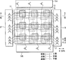
近年来,提出了各种器件构造或电路构造的MRAM,其中之一,具有将多个MTJ元件连接到1个开关元件(选择晶体管)的器件构造。该构造,有利于达到单元高密度或读出容限的提高。In recent years, MRAMs with various device structures and circuit structures have been proposed, one of which has a device structure in which a plurality of MTJ elements are connected to one switching element (selection transistor). This structure is advantageous for achieving high cell density or improving readout margin.
例如,梯形单元构造中,在上部线与下部线之间并联连接多个MTJ元件。如图1所示,该单元构造中,在衬底上边多层(本例中,为4层)叠置多个MTJ元件10。并且,在各层中,将多个MTJ元件10并联连接到上部线11与下部线12之间。For example, in a trapezoidal cell structure, a plurality of MTJ elements are connected in parallel between an upper line and a lower line. As shown in FIG. 1, in this cell structure, a plurality of
上部线11沿X方向延伸,其一端连到选择晶体管14。下部线12也沿X方向延伸,其一端连到读出放大器(S/A)15等外围电路。本例中,读出电流沿着上部线11、MTJ元件10、下部线12的路径,即,沿X方向流动。写入线13与MTJ元件10邻接进行配置,并沿Y方向延伸。The
图2的单元构造是将图1下部线与写入线一体化的例子。即,下部线12沿Y方向延伸,其一端连到读出放大器(S/A)。写入时下部线12起写入线功能,读出时,下部线12起读出(read)线功能。即,读出电流首先流入上部线(X方向)11,而后,经由MTJ元件10流到下部线(Y方向)12。The cell structure in FIG. 2 is an example in which the lower line in FIG. 1 and the write line are integrated. That is, the
磁随机存取存储器的基本构造是,每1个MTJ元件对应1个开关元件(选择晶体管)的1单元-1晶体管构造。但是,多层叠置MTJ元件的器件构造中,如果每1个MTJ元件对应1个开关元件的话,开关元件数就不断增加,将不利于单元高密度化。The basic structure of the magnetic random access memory is a 1-cell-1-transistor structure in which one MTJ element corresponds to one switching element (select transistor). However, in a device structure in which MTJ elements are stacked in multiple layers, if one switching element corresponds to one MTJ element, the number of switching elements will increase, which is not conducive to high cell density.
因此,采用多层叠置MTJ元件10的器件构造场合,即使每1个MTJ元件不对应1个开关元件,也采用能进行读出动作或写入动作这样的器件构造。Therefore, when a device structure in which
例如,图1和图2中表示的器件构造中,对于MTJ元件10的阵列各层,把多个MTJ元件10连接到上部线11与下部线12之间。而且,例如,将选择晶体管14连接到上部线11的一端,将读出放大器(S/A)15连接到下部线12的一端。For example, in the device configuration shown in FIGS. 1 and 2 , a plurality of
可是,这时,图1的例子中,在MTJ元件10的阵列各层上,需要配置上部线(读出/写入线)11、下部线(读出线)12和写入线13总计3条线,并且,图2的例子中,MTJ元件10的各层上,需要配置上部线(读出/写入线)11和下部线(读出/写入线)12总计2条线。However, at this time, in the example of FIG. 1 , on each layer of the array of the
而且,在衬底上边多层叠置的MTJ元件阵列内,配置这种写入线或读出线(电流总线)时,随着MTJ元件的叠置数继续增多,器件构造将复杂化,而且,因制造步骤数的增大而引起工艺成本增加就成了问题。Moreover, in the MTJ element array stacked in multiple layers on the substrate, when disposing such a writing line or a reading line (current bus), as the stacking number of MTJ elements continues to increase, the device structure will be complicated, and, An increase in process cost due to an increase in the number of manufacturing steps becomes a problem.
并且,MTJ元件的特性,受其配置的表面(底膜)的平整度影响很大。该平整度因MTJ元件的叠置数越多越恶化,所以随MTJ元件的叠置数增加,MTJ元件特性的恶化变成问题。Furthermore, the characteristics of the MTJ element are greatly influenced by the flatness of the surface (base film) on which it is placed. This flatness deteriorates as the number of stacked MTJ elements increases, and therefore deterioration of the characteristics of the MTJ element becomes a problem as the number of stacked MTJ elements increases.
(2)概要(2) Summary
本发明例(共用布线)应用于具有多层叠置MTJ元件阵列构造的磁随机存取存储器。本发明例的磁随机存取存储器的特征是,在由上下方向邻接的2个MTJ元件共用1个MTJ元件上需要的2条写入线中的1条。并且,2个MTJ元件相对于共用的1条写入线为对称配置。The example of the present invention (shared wiring) is applied to a magnetic random access memory having a multilayer stacked MTJ element array structure. The magnetic random access memory of the example of the present invention is characterized in that two MTJ elements adjacent to each other in the vertical direction share one of the two write lines required for one MTJ element. In addition, two MTJ elements are arranged symmetrically with respect to one common write line.
因此,可以减少MTJ元件阵列内配置的导线数,能够达到因制造步骤数削减而降低工艺成本。并且,也能抑制伴随MTJ元件叠置数增加带来的平整度恶化,能够提高MTJ元件的特性。Therefore, the number of wires arranged in the MTJ element array can be reduced, and the process cost can be reduced by reducing the number of manufacturing steps. Furthermore, it is also possible to suppress the deterioration of the flatness accompanying the increase in the number of stacked MTJ elements, and to improve the characteristics of the MTJ elements.
(3)实施例(3) Example
①第1实施例①First embodiment
图3表示本发明第1实施例的磁随机存取存储器的单元阵列部分。FIG. 3 shows a cell array portion of the magnetic random access memory according to the first embodiment of the present invention.
半导体衬底上边,把多个MTJ元件叠置成多层(本例中,为4层)。并且,各层中,MTJ元件10在X-Y平面内构成阵列。图3中,省去了有关沿Y方向的MTJ元件列。On the semiconductor substrate, a plurality of MTJ elements are stacked in multiple layers (in this example, 4 layers). Furthermore, in each layer, the
写入线13配置在上下方向邻接的2个MTJ元件10之间,并沿Y方向延伸着。而且,本例中,因为由上下方向邻接的2个MTJ元件共用写入线13,所以采用以下这样的单元构造。即,写入线13不是在全部的层之间配置,而是例如,从半导体衬底一侧数起,配置在奇数层的MTJ元件10正上方,但在偶数层的MTJ元件10正下方。The
本例中,从半导体衬底一侧数起,在第1层MTJ元件与第2层MTJ元件之间和第3层MTJ元件与第4层MTJ元件之间,分别配置写入线13。即,从半导体衬底一侧数起,第2层MTJ元件与第3层MTJ元件之间没有配置写入线13。In this example, counting from the semiconductor substrate side, write
并且,本例中,相对于写入线13,对称配置其上下存在的2个MTJ元件。In addition, in this example, two MTJ elements existing above and below the
即,MTJ元件10是由两层磁性层(强磁性层)和夹于其间的绝缘层(隧道势垒)构成,两层磁性层中固定自旋方向的固定层(或称钉扎层),被配置在远离写入线13的位置。并且,两层磁性层中能自由改变自旋方向的自由层被配置在靠近写入线13的位置。写入线13位于距该上下存在的2个MTJ元件10等距离的位置离开这2个MTJ元件。That is, the
各层中,MTJ元件10的固定层上连接有起读出线功能的第1导电线11A。第1导电线11A为沿X方向延伸,而且,共同连接到X方向配置的多个MTJ元件10的固定层。读出放大器(S/A)15连接到第1导电线11A的一端。Among the layers, the pinned layer of the
并且,各层中,起写入线和读出线功能的第2导电线12A连接到MTJ元件10的自由层。第2导电线12A沿X方向延伸,而且,共同连接到X方向配置的多个MTJ元件10的自由层。起选择晶体管功能的选择晶体管14连接到第2导电线12A的一端。Furthermore, in each layer, a second
按照这种第1实施例的单元构造,为了给1个MTJ元件写入数据,由上下方向邻接的2个MTJ元件,使需要2条写入线之中的1条共有化。因此,可以减少MTJ元件阵列内所配置的导线数,能够达到因制造步骤次数的削减而降低工艺成本。并且,也能抑制伴随MTJ元件的叠置数增加带来的平整度恶化,可以提高MTJ元件特性。According to the cell structure of the first embodiment, in order to write data into one MTJ element, one of the two writing lines is required to be shared by the two vertically adjacent MTJ elements. Therefore, the number of wires arranged in the MTJ element array can be reduced, and the process cost can be reduced by reducing the number of manufacturing steps. In addition, it is also possible to suppress the deterioration of the flatness accompanying the increase in the number of stacked MTJ elements, and to improve the characteristics of the MTJ element.
并且,按照第1实施例的单元构造,把配置于写入线上下的2个MTJ元件配置成使其对于该写入线互相对称。因此,关于由写入线中流动的电流发生的磁场,作用于其上下配置的2个MTJ元件自由层的磁场强度实质上变成相同,能够控制作用于各MTJ元件的磁场离散。Furthermore, according to the cell structure of the first embodiment, the two MTJ elements arranged above and below the write line are arranged symmetrically with respect to the write line. Therefore, with regard to the magnetic field generated by the current flowing in the write line, the magnetic field strengths acting on the free layers of the two MTJ elements arranged above and below the same become substantially the same, and the dispersion of the magnetic field acting on each MTJ element can be controlled.
②第2实施例②Second embodiment
图4表示本发明第2实施例的磁随机存取存储器的单元阵列部分。FIG. 4 shows a cell array portion of a magnetic random access memory according to a second embodiment of the present invention.
本实施例的磁随机存取存储器的特征是,与图3的磁随机存取存储器比较时,省略图3的读出线12A,使图3的写入线13具有读出线的功能。Compared with the magnetic random access memory of FIG. 3, the magnetic random access memory of this embodiment is characterized in that the read
在半导体衬底上,把多个MTJ元件10叠置成多层(本例中,为4层)。并且,各层中,MTJ元件10在X-Y平面内构成阵列。图4中,省去了有关沿Y方向的MTJ元件列。On a semiconductor substrate, a plurality of
各层中,MTJ元件10的自由层上连接省起写入线和读出线功能的第1导电线11A。第1导电线11A沿X方向延伸,而且,共同连接到X方向配置的多个MTJ元件10的自由层。第1导电线11A的一端,连接有作为选择晶体管的选择晶体管14。Among the layers, the free layer of the
并且,各层中,MTJ元件10的固定层上连接有起写入线和读出线功能的第2导电线12A。第2导电线12A沿Y方向延伸,而且,共同连接到Y方向配置的多个MTJ元件10的固定层。读出放大器(S/A)15连接到第2导电线12A的一端。Furthermore, among the layers, the second
第2导电线12A被配置在上下方向邻接的2个MTJ元件10之间。即,第2导电线12A被其上下方向邻接的2个MTJ元件所共用。为此,第2导电线12A不是配置于全部的层之间,而是配置于例如,从半导体衬底一侧数起,第奇数个MTJ元件10正上方,而且,在第偶数个MTJ元件10正下方。The second
本例中,从半导体衬底一侧数起,在第1层MTJ元件与第2层MTJ元件之间和第3层MTJ元件与第4层MTJ元件之间,分别配置第2导电线12A。即,从半导体衬底一侧数起,第2层MTJ元件与第3层MTJ元件之间没有配置第2导电线12A。In this example, counting from the side of the semiconductor substrate, the second
并且,本例中,相对于第2导电线12A,对称配置其上下存在的2个MTJ元件。即,MTJ元件10是由两层磁性层(强磁性层)和夹于其间的绝缘层(隧道势垒)构成,2个磁性层中固定自旋方向的固定层,被配置在靠近第2导电线12A的位置。并且,两层磁性层中能自由改变自旋方向的自由层,被配置在远离第2导电线12A的位置。In addition, in this example, two MTJ elements existing above and below the second
按照这种第2实施例的单元构造,为了给1个MTJ元件写入数据,由上下方向邻接的2个MTJ元件,使需要2条写入线之中的1条共有化。因此,不用写入专用的导线或读出专用的导线,把1条导线使用于写入和读出,所以能够大幅度减少导线数。本例中,对1个MTJ元件的导线数实质上为1.5条。因此,能够达到因制造步骤次数的削减而降低工艺成本。并且,也能抑制伴随MTJ元件的叠置数增加带来的平整度恶化,可以提高MTJ元件特性。According to the cell structure of the second embodiment, in order to write data into one MTJ element, one of the two writing lines required to be shared by two vertically adjacent MTJ elements is shared. Therefore, a single wire is used for writing and reading without using a wire dedicated to writing or a wire dedicated to reading, so that the number of wires can be significantly reduced. In this example, the number of wires for one MTJ element is substantially 1.5. Therefore, it is possible to reduce the process cost by reducing the number of manufacturing steps. In addition, it is also possible to suppress the deterioration of the flatness accompanying the increase in the number of stacked MTJ elements, and to improve the characteristics of the MTJ element.
并且,按照第2实施例,把配置于写入线上下的2个MTJ元件配置成使其对于该写入线互相对称。因此,关于由写入线中流动的电流发生的磁场,作用于其上下配置的2个MTJ元件自由层的磁场强度,基本上变成相同,能够控制作用于各MTJ元件的磁场离散。Furthermore, according to the second embodiment, the two MTJ elements arranged above and below the writing line are arranged symmetrically with respect to the writing line. Therefore, with regard to the magnetic field generated by the current flowing in the write line, the strength of the magnetic field acting on the free layers of the two MTJ elements arranged above and below becomes substantially the same, and the dispersion of the magnetic field acting on each MTJ element can be controlled.
③第3实施例③The third embodiment
图5表示本发明第3实施例磁的随机存取存储器的单元阵列部分。FIG. 5 shows a cell array portion of a magnetic random access memory according to a third embodiment of the present invention.
本实施例的磁随机存取存储器的特征是,与图4的磁随机存取存储器比较时,图4的第1导电线(写入线和读出线)11A被其上下方向邻接的2个MTJ元件所共用。The magnetic random access memory of this embodiment is characterized in that, when compared with the magnetic random access memory of FIG. 4, the first conductive line (writing line and reading line) 11A of FIG. shared by MTJ elements.
半导体衬底上边,把多个MTJ元件叠置成多层(本例中,为8层)。并且,各层中,MTJ元件10在X-Y平面内构成阵列。图5中,省去了有关沿Y方向的MTJ元件列。On the semiconductor substrate, a plurality of MTJ elements are stacked in multiple layers (eight layers in this example). Furthermore, in each layer, the
各层中,MTJ元件10的自由层上,连接有起写入线和读出线功能的第1导电线11A。第1导电线11A沿X方向延伸,而且,共同连接到X方向配置的多个MTJ元件10的自由层。第1导电线11A的一端,连接有作为选择晶体管的选择晶体管14。Among the layers, the free layer of the
第1导电线11A被配置在上下方向邻接的2个MTJ元件10之间。即,第1导电线11A被其上下方向邻接的2个MTJ元件所共用。为此,第1导电线11A,不是配置于全部的层之间,而是配置于例如,从半导体衬底一侧数起,第奇数个MTJ元件10的正下方,而且,在第偶数个MTJ元件10的正上方。The first
本例中,从半导体衬底一侧数起,在第1层MTJ元件的正下方与第2层MTJ元件和第3层MTJ元件之间、第4层MTJ元件与第5层MTJ元件之间,第6层MTJ元件与第7层MTJ元件之间。第8层MTJ元件的正上方,分别配置第1导电线11A。In this example, counting from the side of the semiconductor substrate, directly below the MTJ element on the first layer, between the MTJ element on the second layer and the MTJ element on the third layer, and between the MTJ element on the fourth layer and the MTJ element on the fifth layer , Between the 6th layer MTJ element and the 7th layer MTJ element. Immediately above the 8th-layer MTJ elements, the first
并且,本例中,相对于第1导电线11A,对称配置其上下存在的2个MTJ元件。即,MTJ元件10是由两层磁性层(强磁性层)和夹于其间的绝缘层(隧道势垒)构成,两层磁性层中固定自旋方向的固定层,被配置在远离第1导电线11A的位置。并且,两层磁性层中能自由改变自旋方向的自由层,被配置在离第1导电线11A很近的位置。In addition, in this example, two MTJ elements existing above and below the first
并且,各层中,MTJ元件10的固定层上,连接有起写入线和读出线功能的第2导电线12A。第2导电线12A沿Y方向延伸,而且,共同连接到沿Y方向配置的多个MTJ元件10的固定层。读出放大器(S/A)15连接到第2导电线12A的一端。Furthermore, in each layer, the second
第2导电线12A被配置在上下方向邻接的2个MTJ元件10之间。即,第2导电线12A被其上下方向邻接的2个MTJ元件所共用。为此,第2导电线12A不是配置于全部的层之间,而是配置于例如,从半导体衬底一侧数起,第奇数个MTJ元件10的正上方,而且,在第偶数个MTJ元件10的正下方。The second
本例中,从半导体衬底一侧数起,在第1层MTJ元件与第2层MTJ元件之间、第3层MTJ元件与第4层MTJ元件之间、第5层MTJ元件与第6层MTJ元件之间、以及第7层MTJ元件与第8层MTJ元件之间,分别配置第2导电线12A。In this example, counting from the side of the semiconductor substrate, between the MTJ elements of the first layer and the MTJ elements of the second layer, between the MTJ elements of the third layer and the MTJ elements of the fourth layer, between the MTJ elements of the fifth layer and the sixth Second
并且,本例中,相对于第2导电线12A,对称配置其上下存在的2个MTJ元件。即,MTJ元件10是由两层磁性层(强磁性层)和夹于其间的绝缘层(隧道势垒)构成,两层磁性层中固定自旋方向的固定层,被配置在靠近第2导电线12A的位置。并且,两层磁性层中能自由改变自旋方向的自由层,被配置在远离第2导电线12A的位置。In addition, in this example, two MTJ elements existing above and below the second
按照这种第3实施例的单元构造,把连接MTJ元件自由层的导线和连接固定层的导线,规定可用作写入线和读出线,而且,由上下方向邻接的2个MTJ元件共用。According to the cell structure of the third embodiment, the wires connected to the free layer of the MTJ element and the wires connected to the fixed layer are prescribed to be used as write lines and read lines, and are shared by two adjacent MTJ elements in the vertical direction. .
因此,可以大幅度减少MTJ元件阵列内配置的导线数,能够达到因制造步骤次数的削减而降低工艺成本。并且,也能抑制伴随MTJ元件的叠置数增加带来的平整度恶化,可以提高MTJ元件特性。Therefore, the number of wires arranged in the MTJ element array can be greatly reduced, and the process cost can be reduced due to the reduction of the number of manufacturing steps. In addition, it is also possible to suppress the deterioration of the flatness accompanying the increase in the number of stacked MTJ elements, and to improve the characteristics of the MTJ element.
并且,按照第3实施例的单元构造,把配置于写入线上下的2个MTJ元件配置成使其对于该写入线互相对称。因此,关于由写入线中流动的电流发生的磁场,作用于其上下配置的2个MTJ元件自由层的磁场强度,实质上变成相同,能够控制作用于各MTJ元件的磁场离散。Furthermore, according to the cell structure of the third embodiment, the two MTJ elements arranged above and below the write line are arranged symmetrically with respect to the write line. Therefore, with regard to the magnetic field generated by the current flowing in the write line, the strength of the magnetic field acting on the free layers of the two MTJ elements arranged above and below becomes substantially the same, and the dispersion of the magnetic field acting on each MTJ element can be controlled.
(4)其它(4) Others
上述第1到第3实施例中,对多层叠置MTJ元件的阵列构造的各层,都将X方向或Y方向的MTJ元件上共同连接写入线(或读出线)的器件作为前提进行说明,但是本发明的应用不限于这样的器件。In the above-mentioned first to third embodiments, for each layer of the array structure of multi-layer stacked MTJ elements, the MTJ elements in the X-direction or Y-direction are all connected to the MTJ elements in the X direction or Y direction. illustration, but the application of the present invention is not limited to such devices.
本发明只要是具有多层叠置MTJ元件阵列构造的磁随机存取存储器,也都可能应用于这样构造的器件。As long as the present invention is a magnetic random access memory with a multi-layer stacked MTJ element array structure, it may also be applied to devices with such a structure.
并且,上述的第1到第3实施例中,与MTJ元件阵列内导线连接的晶体管一般的是MOS晶体管,但也可以是双极晶体管或二极管。In addition, in the above-mentioned first to third embodiments, the transistors connected to the wires in the MTJ element array are generally MOS transistors, but they may also be bipolar transistors or diodes.
(5)结束语(5) Conclusion
以上,如说明的那样,按照本发明例的磁随机存取存储器,采用在其上下存在的MTJ元件之间共用写入线的至少1条的办法,可以减少MTJ元件阵列内配置的导线数,能够达到因制造步骤次数的削减而降低工艺成本。并且,因为减少MTJ元件阵列内配置的导线数,所以能够抑制伴随MTJ元件的叠置数增加带来的平整度恶化,可以提高MTJ元件特性。As described above, according to the magnetic random access memory of the example of the present invention, by sharing at least one writing line between the MTJ elements existing above and below, the number of wires arranged in the MTJ element array can be reduced, The process cost can be reduced due to the reduction of the number of manufacturing steps. In addition, since the number of wires arranged in the MTJ element array is reduced, deterioration of flatness due to an increase in the number of stacked MTJ elements can be suppressed, and the characteristics of the MTJ element can be improved.
2.串联(蛇形)/并联连接布线2. Serial (serpentine)/parallel connection wiring
(1)背景技术(1) Background technology
磁随机存取存储器的基本构造是,1个MTJ元件对应1个开关元件(选择晶体管)的1单元-1晶体管构造。但是,多层叠置MTJ元件的器件构造中,如果1个MTJ元件对应1个开关元件的话,开关元件数就不断增加,将不利于单元高密度化。The basic structure of a magnetic random access memory is a 1-cell-1-transistor structure in which one MTJ element corresponds to one switching element (select transistor). However, in the device structure of stacking MTJ elements in multiple layers, if one MTJ element corresponds to one switching element, the number of switching elements will continue to increase, which is not conducive to high cell density.
因此,在多层叠置MTJ元件10的器件构造场合,即使1个MTJ元件不对应1个开关元件,也采用能进行读出动作或写入动作这样的器件构造。Therefore, in the case of a device structure in which
例如,图1和图2中表示的器件构造中,对于MTJ元件10的阵列各层,把多个MTJ元件10连接到上部线11与下部线12之间。而且,例如,将选择晶体管14连接到上部线11的一端,将读出放大器(S/A)15连接到下部线12的一端。For example, in the device configuration shown in FIGS. 1 and 2 , a plurality of
可是,这时,图1的例子中,对于各个MTJ元件10的阵列各层上配置的上部线11就需要选择晶体管。并且,如图6所示,上部线11在MTJ元件10的阵列16上边,沿X方向延伸。即,规定集中于阵列16的端部区域17,配置连接到上部线11的选择晶体管。However, in this case, in the example of FIG. 1 , selection transistors are required for the
同样,对于各个在MTJ元件10的阵列各层上配置的下部线(读出线)12就需要读出放大器(晶体管)。即,如图6所示,下部线12在MTJ元件10的阵列16上边沿X方向延伸,所以规定集中于阵列16的端部区域18,配置连接到下部线12的选择晶体管。Likewise, sense amplifiers (transistors) are required for each lower line (sense line) 12 disposed on each layer of the array of
同样,对于各个在MTJ元件10的阵列各层上配置的写入线13,也需要选择晶体管。即,如图6所示,写入线13在MTJ元件10的阵列16上边沿Y方向延伸,所以规定集中于阵列16的端部区域19A、19B,配置连接到写入线13的选择晶体管。Similarly, selection transistors are required for each of the
尽管,大家都知道,在对MTJ元件的数据写入/读出动作的方面,起因于MTJ元件的特性,需要大电流。因此,可以预料,连接到下部线12和写入线13的晶体管尺寸必然需要增大。However, it is well known that a large current is required due to the characteristics of the MTJ element in the data writing/reading operation to the MTJ element. Therefore, it can be expected that the size of the transistors connected to the
因而,配置用于在阵列16外围配置电流驱动晶体管的区域17、18、19A、19B的面积也将增大,无法实现芯片尺寸的缩小、每芯片制造成本的降低等。并且,因为MTJ元件与叠置数成比例,选择晶体管的个数也增加,MTJ元件叠置个数变成非常多的话,在选择晶体管的布局方面需要很多时间,开发时间就拉长了。Therefore, the area of the
(2)概要(2) Summary
本发明例(串联/并联连接布线)将应用于具有多层叠置MTJ元件阵列构造的磁随机存取存储器。The example of the present invention (series/parallel connection wiring) will be applied to a magnetic random access memory having a multilayer stacked MTJ element array structure.
本发明例的磁随机存取存储器的特征是,在MTJ元件阵列的1行或1列内,串联或并联连接1层中每1个配置有相同功能的多条导线(例如,写入线、读出线等)。这时,对串联/并联连接的导线而言,其一端只要配置1个,或,其两端各配置1个晶体管就行,因而可以减少MTJ元件阵列端部配置的晶体管数。The magnetic random access memory of the example of the present invention is characterized in that in one row or one column of the MTJ element array, a plurality of wires (for example, write lines, readout line, etc.). In this case, only one transistor is arranged at one end of the wires connected in series/parallel, or one transistor is arranged at each of the two ends, so that the number of transistors arranged at the ends of the MTJ element array can be reduced.
并且,按照本发明例的器件构造,不管MTJ元件的叠置数,只要把晶体管连接到MTJ元件阵列内的1行或1列内串联或并联连接的导线上就行,所以即使增加MTJ元件的叠置数,增大存储器容量,既没有增加晶体管数,也不会使其布局复杂化。And, according to the device structure of the example of the present invention, regardless of the number of stacked MTJ elements, it is enough to connect the transistors to the wires connected in series or in parallel in one row or one column of the MTJ element array, so even if the stacked number of MTJ elements is increased, Set the number and increase the memory capacity without increasing the number of transistors or complicating the layout.
进而,在MTJ元件布局的1行或1列内,不管MTJ元件的叠置数,晶体管数常常固定,所以把MTJ元件阵列制成1个小块,集合多个块成为大的存储单元阵列也行。这时,MTJ元件阵列的正下方,可以配置晶体管或读出放大器等的核心电路。Furthermore, in one row or one column of the MTJ element layout, the number of transistors is always fixed regardless of the stacked number of MTJ elements. Therefore, it is also possible to form an MTJ element array into a small block and assemble multiple blocks to form a large memory cell array. OK. At this time, core circuits such as transistors and sense amplifiers can be placed directly under the MTJ element array.
(3)实施例(3) Example
①第1实施例①First embodiment
图7表示本发明第1实施例磁随机存取存储器的单元阵列部分布局。图8表示沿图7的单元阵列部分的X方向剖面图,即,沿图7的VIII-VIII线的剖面图。FIG. 7 shows the partial layout of the cell array of the magnetic random access memory according to the first embodiment of the present invention. FIG. 8 shows a cross-sectional view along the X direction of the cell array portion of FIG. 7 , that is, a cross-sectional view along line VIII-VIII of FIG. 7 .
在半导体衬底上边,把多个MTJ元件10叠置成多层(本例中,为3层)。并且,各层中,MTJ元件10在X-Y平面内构成阵列。On the semiconductor substrate, a plurality of
上部线11和下部线12一起沿X方向延伸,并在两线11、12之间,配置沿X方向配置的多个MTJ元件10。上部线11的一端,连接有选择晶体管14。并且,下部线12的一端,连接有读出放大器(S/A)15等的外围电路。The
本实施例中,上部线11和下部线12起读出线功能。即,读出数据时,读出电流沿着上部线11、MTJ元件10、下部线12这样的路径,即,沿X方向流动。In this embodiment, the
就具体的读出方法来说,首先,在上部线11和下部线12中流动读出电流,例如,用读出放大器,检测这时的下部线12电位。其次,给选定的MTJ元件(存储单元)写入规定数据(“0”或“1”),而后,再次在上部线11和下部线12中流动读出电流,用读出放大器,检测这时的下部线12的电位。在第1次和第2次的读出中,如果用读出放大器检出的电位相同,那么就将选定的MTJ元件数据判断为与规定数据相同,如果不同,则选定的MTJ元件数据判断为与规定数据不同。最后,给选定的MTJ元件重新写入正确的数据。In a specific read method, first, a read current is passed through the
在MTJ元件10阵列的各层,写入线13被配置在MTJ元件10上边,并沿Y方向延伸。并且,写入线13接近MTJ元件10的自由层进行配置。进而,把沿X方向配置的多个MTJ元件构成的组规定为1列,把沿Y方向偏置的多个MTJ元件构成的组规定为1行的场合,本例中,MTJ元件10阵列的1行内,串联连接各层配置的写入线13。In each layer of the
即,如图9所示,在MTJ元件10阵列的端部,通过接触塞,把上层的写入线13与下层的写入线13互相电连接起来。图9中,为了简化,省去了上部线和下部线。That is, as shown in FIG. 9, at the end of the
就具体的写入方法来说,例如,在作为写入线功能的选定1列内的下部线12里,根据写入数据值,流动向着一方向或另一方向的写入电流。同时,在选定1行内的写入线13里流动向着一方向的写入电流。因此,给配置于下部线12与写入线13之间的MTJ元件(存储单元)10写入规定数据。As for a specific writing method, for example, in the
这样,本实施例中,MTJ元件10阵列的1行内,采用各层配置具有同样功能的线,即,串联地连接的写入线的办法,对该写入线,只要其两端每端配置1个晶体管就行。因此,能够大幅度减少MTJ元件10的阵列16的端部区域19A、19B上配置的晶体管数。In this way, in this embodiment, in one row of the
并且,按照这种器件构造,不管MTJ元件10的叠置数,MTJ元件10的阵列16的1行内,只要把晶体管连接到串联连接的导线上就行,即使增加MTJ元件10的叠置数,谋求存储容量的增大,也没有增加晶体管,也不会使其布局复杂化。Moreover, according to this device structure, regardless of the number of
进而,连接到MTJ元件10的阵列16的行内各层中配置的写入线13的晶体管数常常为固定,所以把MTJ元件10的阵列16制成1个小块,集合多个块构成大的存储单元阵列也行。这时,如图9所示,各块内MTJ元件10的正下方,可以配置晶体管或读出放大器等的核心电路。Furthermore, the number of transistors connected to the
另外,图7中,记载着叠置的的MTJ元件、沿X方向延伸和沿Y方向洋使的线,各自在各层内使其互相偏移,这是为了分开容易说明的缘故,实际上不管互相偏移,或完全重叠,哪种也都可以。In addition, in FIG. 7, it is described that the stacked MTJ elements, the lines extending in the X direction and extending in the Y direction are each offset from each other in each layer. This is for the sake of separation and ease of description. In fact, It doesn't matter if they are offset from each other, or completely overlap, whichever is fine.
②第2实施例②Second embodiment
图10表示本发明第2实施例的磁随机存取存储器的单元阵列部分。FIG. 10 shows the cell array portion of the magnetic random access memory according to the second embodiment of the present invention.
本实施例的磁随机存取存储器的特征是,若与图8的磁随机存取存储器比较,把图8的MTJ元件10叠置数分成4层。至于其它方面,成为与图8的磁随机存取存储器同样。The magnetic random access memory of this embodiment is characterized in that, compared with the magnetic random access memory of FIG. 8 , the number of
在半导体衬底上边,把多个MTJ元件叠置成多层(本例中,为4层)。并且,各层中,MTJ元件10在X-Y平面内构成阵列。On the semiconductor substrate, a plurality of MTJ elements are stacked in multiple layers (in this example, 4 layers). Furthermore, in each layer, the
上部线11和下部线12一起沿X方向延伸,并在两线11、12之间,配置沿X方向配置的多个MTJ元件10。上部线11的一端,连接有选择晶体管14。并且,下部线12的一端,连接有读出放大器(S/A)15等的外围电路。The
上部线11和下部线12起读出线功能。即,读出数据时,读出电流沿着上部线11、MTJ元件10、下部线12这样的路径,即,沿X方向流动。The
在MTJ元件10的阵列各层,写入线13被配置在MTJ元件10上边,并沿Y方向延伸。并且,写入线13接近MTJ元件10的自由层进行配置。进而,把沿X方向配置的多个MTJ元件构成的组规定为1列,把沿Y方向偏置的多个MTJ元件构成的组规定为1行的场合,本例中,MTJ元件10的阵列1行内,串联连接各层配置的写入线13。In each layer of the array of
即,如图11所示,在MTJ元件10的阵列端部,通过接触塞,把上层的写入线13与下层的写入线13互相电连接起来,图11中,为了简化,省去了上部线和下部线。That is, as shown in FIG. 11, at the end of the array of
本实施例中,MTJ元件10的叠置数为4层。即,MTJ元件10的叠置数为偶数层(2、4、6、…层)的场合,如图1所示,将用于连接写入线13和晶体管的2个接触部分,一起配置在MTJ元件10阵列部的一个端部。In this embodiment, the number of
这时,如图11所示,例如,在邻接块BK0的块BK1阵列的正下方,配置与块BK0内写入线13的一端连接的晶体管,并在块BK0陈列的正下方,配置与块BK0内写入线13的另一端连接的晶体管。At this time, as shown in FIG. 11, for example, directly under the block BK1 array adjacent to block BK0, a transistor connected to one end of the
另外,正如上述第1实施例一样,MTJ元件10的叠置数为奇数层(3、5、7、…层)的场合,如图9所示,在MTJ元件10阵列部分的一个端部配置用于连接写入线13的一端和晶体管的接触部,在与MTJ元件10阵列部分的一端部对向的另一端部配置用于连接写入线13另一端和晶体管的接触部。In addition, as in the above-mentioned first embodiment, when the stacked number of
于是,这时,如图9所示,例如,在块BK0的阵列的正下方,各自配置连接块BK0内的写入线13一端和另一端的晶体管。Therefore, at this time, as shown in FIG. 9 , for example, transistors connecting one end and the other end of the
这样,本实施例中,MTJ元件10阵列的1行内,采用各层配置具有同样功能的线,即,串联地连接的写入线的办法,对该写入线,只要其两端每端配置1个晶体管就行。因此,能够大幅度减少MTJ元件10的阵列16的端部配置的晶体管数。In this way, in this embodiment, in one row of the
并且,按照这种器件构造,不管MTJ元件10的叠置数,MTJ元件10的阵列1行内,只要把晶体管连接到串联连接的导线上就行,所以即使增加MTJ元件10的叠置数,谋求存储容量的增大,也没有增加晶体管,也不会使其布局复杂化。Moreover, according to this device structure, regardless of the number of
进而,连接到MTJ元件10的阵列行内的各层中配置的写入线13的晶体管数常常为固定,所以把MTJ元件10的阵列制成1个小块,集合多个块构成大的存储单元阵列也行。这时,如图11所示,各块内MTJ元件10的正下方,可以配置晶体管或读出放大器等的核心电路。Furthermore, the number of transistors connected to the
③第3实施例③The third embodiment
图12表示本发明第3实施例的磁随机存取存储器的单元阵列部分。FIG. 12 shows a cell array portion of a magnetic random access memory according to a third embodiment of the present invention.
本实施例的磁随机存取存储器的特征是,若与图10的磁随机存取存储器比较,对每1层改变图10的MTJ元件10的固定层磁化方向,至于其它方面,都与图10的磁随机存取存储器同样。The magnetic random access memory of this embodiment is characterized in that, compared with the magnetic random access memory of FIG. 10, the magnetization direction of the fixed layer of the
在半导体衬底上边,把多个MTJ元件叠置成多层(本例中,为4层)。并且,各层中,MTJ元件10在X-Y平面内构成阵列。On the semiconductor substrate, a plurality of MTJ elements are stacked in multiple layers (in this example, 4 layers). Furthermore, in each layer, the
上部线11和下部线12一起沿X方向延伸,并在两线11、12之间,配置沿X方向配置的多个MTJ元件10。上部线11的一端,连接有选择晶体管14。并且,下部线12的一端,连接有读出放大器(S/A)15等的外围电路。The
上部线11和下部线12起读出线功能。即,读出数据时,读出电流沿着上部线11、MTJ元件10、下部线12这样的路径,即,沿X方向流动。The
在MTJ元件10的阵列各层,写入线13被配置在MTJ元件10上,并沿Y方向延伸。并且,写入线13接近MTJ元件10的自由层进行配置。进而,把沿X方向配置的多个MTJ元件构成的组规定为1列,把沿Y方向偏置的多个MTJ元件构成的组规定为1行的场合,本例中,MTJ元件10的阵列1行内,串联连接各层配置的写入线13。In each layer of the array of
即,如图11所示,在MTJ元件10的阵列端部,通过接触塞,把上层的写入线13与下层的写入线13互相电连接起来。That is, as shown in FIG. 11 , at the end of the array of
尽管,上述第2实施例中,由图11很清楚,在Y-Z平面内蛇形配置写入线13。这时,如图12所示,写入线13里流动一个方向电流时,在各层中,写入线13里流动的电流方向,每1层变成互相相反方向。However, in the second embodiment described above, as is clear from FIG. 11, the writing lines 13 are arranged in a serpentine shape in the Y-Z plane. At this time, as shown in FIG. 12, when a current flows in one direction in the
图12的场合,对第奇数层的写入线13,即,最靠近半导体衬底的第1层的写入线13和第3层的写入线13来说,从纸面表面向内流动写入电流,对第偶数层的写入线13,即,第2层和第4层的写入线13来说,从纸面内向外表面流动写入电流。In the case of FIG. 12 , for the
在这种状况下,例如,假设全部MTJ元件10的固定层磁化方向都是相同的,例如,给第奇数层的MTJ元件和第偶数层的MTJ元件写入相同数据的场合,写入线13里应该流动不同方向的写入电流。In this situation, for example, assuming that the magnetization directions of the pinned layers of all
即,全部MTJ元件10的固定层磁化方向为相同,下部线12的写入电流方向为一定的场合,如要是写入线13里只流动一个方向的写入电流的话,那么各层MTJ元件10的自由层磁化方向,对每层变成相反方向。即,各层MTJ元件10的磁化状态,对每1层,变成平行、反平行,也不管同样动作,对于各层的MTJ元件10,写入不同的数据。That is, when the magnetization directions of the pinned layers of all
这样,第2实施例中,写入线13里流动一方向电流的场合,各层中,流过写入线13的电流变成互相相反方向,所以有可能使写入动作的控制方法复杂化。In this way, in the second embodiment, when a current flows in one direction in the
因此,本实施例中,为了解决这种事情,如图12所示,提出每1层改变MTJ元件10的固定层磁化方向的方案。这时,如果写入线13里只流动一方向写入电流,各层MTJ元件10的自由层磁化方向,对每1层都变成相反方向,而各层MTJ元件10的磁化状态对于各层变成相同(平行或反平行)。即,给各层的MTJ元件10,写入同样数据。Therefore, in this embodiment, in order to solve this problem, it is proposed to change the magnetization direction of the pinned layer of the
关于MTJ元件10的固定层磁化方向,按照现有的工艺,能够很容易对每1层改变磁化方向。即,为了使每1层变更MTJ元件10的固定层磁化方向,淀积构成固定层的材料时,就可以调整磁场的方向。Regarding the magnetization direction of the pinned layer of the
另外,本实施例中,通过对每1层变更MTJ元件10的固定层磁化方向,解决写入线13蛇形变动的问题,但除此以外,也有几个解决方法。In addition, in this embodiment, the problem of the serpentine variation of the
例如,虽然写入控制变为复杂,但是如上述那样,也可以一面给写入线13流动不同方向的电流,并且,一面变更流入下部线12的写入电流的方向。并且,可以认为,各层以不同的磁化状态保存同一数据,对各层变更数据判定的条件也行。For example, although the write control becomes complicated, it is also possible to change the direction of the write current flowing into the
这样,本实施例中,变更每1层中MTJ元件的固定层磁化方向。这时,写入线里只流动一方向写入电流的话,各层MTJ元件的自由层磁化方向在每1层就变为相反方向,然而各层的MTJ元件磁化状态,对各层却成了相同(平行或反平行)。Thus, in this embodiment, the magnetization direction of the pinned layer of the MTJ element is changed for each layer. At this time, if only one direction of write current flows in the write line, the magnetization direction of the free layer of the MTJ element of each layer becomes the opposite direction for each layer, but the magnetization state of the MTJ element of each layer is different for each layer. same (parallel or antiparallel).
因而,按照本实施例,获得与上述第2实施例磁的随机存取存储器同样的效果,同时也没有使写入动作的控制方法复杂化。Therefore, according to this embodiment, the same effect as that of the magnetic random access memory of the second embodiment described above can be obtained without complicating the method of controlling the writing operation.
④第4实施例④ Fourth embodiment
图13表示本发明第4实施例的磁随机存取存储器单元阵列部分概要图。图13中,为了简化,省去了连接MTJ元件的上部线和下部线。Fig. 13 is a schematic diagram showing part of the magnetic random access memory cell array according to the fourth embodiment of the present invention. In FIG. 13 , the upper and lower wires connecting the MTJ elements are omitted for simplicity.
本实施例的磁随机存取存储器的特征是,若与图11的磁随机存取存储器比较,不是串联连接,而是并联累进图11的MTJ元件10的各层中配置的写入线13,至于其它方面,都与图11的磁随机存取存储器同样。The magnetic random access memory of this embodiment is characterized in that, compared with the magnetic random access memory of FIG. 11 , the
在半导体衬底上边,把多个MTJ元件叠置成多层(本例中,为4层)。并且,各层中,MTJ元件10在X-Y平面内构成阵列。On the semiconductor substrate, a plurality of MTJ elements are stacked in multiple layers (in this example, 4 layers). Furthermore, in each layer, the
关于本实施例,也如图10所示,上部线11和下部线12一起沿X方向延伸,并在两线11、12之间,配置沿X方向配置的多个MTJ元件10。上部线11的一端,连接有选择晶体管14。并且,下部线12的一端,连接有读出放大器(S/A)15等的外围电路。In this embodiment, as also shown in FIG. 10 , the
如图13所示,在MTJ元件10的阵列各层,写入线13被配置在MTJ元件10上边,并沿Y方向延伸。并且,写入线13接近MTJ元件10的自由层进行配置。进而,把沿X方向配置的多个MTJ元件构成的组规定为1列,把沿Y方向偏置的多个MTJ元件构成的组规定为1行的场合,本例中,MTJ元件10的阵列1行内,并联连接各层配置的写入线13。As shown in FIG. 13 , in each layer of the array of
即,在MTJ元件10的阵列端部,通过接触塞,把上层的写入线13与下层的写入线13互相电连接起来。That is, at the array end of the
尽管,上述的第2实施例中,因为各层的写入线13互相串联连接,从图11很清楚,写入线13在Y-Z平面内为蛇形配置。对此,本实施例中,因为各层的写入线13互相并联连接,从图13很清楚,写入线13在Y-Z平面内呈梯子状。Although, in the above-mentioned second embodiment, since the
本实施例中,写入线13里流动一方向电流的场合,与第2实施例不同,各层中。写入线13里流动的电流方向,成为互相相同方向。In this embodiment, when a current flows in one direction in the
所以,按照本实施例,获得与上述第2实施例的磁随机存取存储器同样的效果,同时如上述第2实施例那样,即使不采取对每1层变更MTJ元件的固定层磁化方向的对策,也容易控制写入动作。Therefore, according to this embodiment, the same effect as that of the magnetic random access memory of the above-mentioned second embodiment is obtained, and at the same time, as in the above-mentioned second embodiment, even without taking measures to change the magnetization direction of the pinned layer of the MTJ element for each layer , It is also easy to control the write operation.
并且,本实施例中,因为各层的写入线并联连接,在与MTJ元件阵列互相对向的2个端部各设置一个写入线与晶体管的接触部。因此,把MTJ元件阵列制成1个小块,集合多个块构成存储单元阵列也行。这时,各块内的MTJ元件阵列的正下方,很容易配置晶体管或读出放大器等的核心电路。Furthermore, in this embodiment, since the write lines of each layer are connected in parallel, one contact between the write line and the transistor is provided at each of the two ends facing the MTJ element array. Therefore, the MTJ element array may be made into one small block, and a plurality of blocks may be combined to form a memory cell array. In this case, it is easy to arrange core circuits such as transistors and sense amplifiers directly under the MTJ element arrays in each block.
⑤第5实施例⑤ Fifth Embodiment
图14表示本发明第5实施例的磁随机存取存储器的单元阵列部分。图15表示沿图14的单元阵列部分的Y方向剖面图。FIG. 14 shows a cell array portion of a magnetic random access memory according to a fifth embodiment of the present invention. FIG. 15 is a sectional view along the Y direction of the cell array portion of FIG. 14 .
第5实施例是组合上述第1实施例与「共用布线」的例子。The fifth embodiment is an example in which the above-mentioned first embodiment and "common wiring" are combined.
在半导体衬底上边,把多个MTJ元件叠置成多层(本例中,为4层)。并且,各层中,MTJ元件10在X-Y平面内构成阵列。On the semiconductor substrate, a plurality of MTJ elements are stacked in multiple layers (in this example, 4 layers). Furthermore, in each layer, the
写入线13配置在上下方向邻接的2个MTJ元件10之间,并沿Y方向延伸。而且,本例中,由上下方向邻接的2个MTJ元件共用写入线13。即,写入线13不是配置在全部层之间,而是例如,从半导体衬底一侧数起,配置于第奇数层的MTJ元件10的正上方和第偶数层的MTJ元件10的正下方。The
并且,把沿X方向配置的多个MTJ元件构成的组规定为1列,把沿Y方向偏置的多个MTJ元件构成的组规定为1行的场合,本例中,MTJ元件10的阵列1行内,把各层配置的写入线13串联连接起来。Furthermore, when defining a group consisting of a plurality of MTJ elements arranged in the X direction as a column, and defining a group consisting of a plurality of MTJ elements offset in the Y direction as a row, in this example, the array of
并且,相对于写入线13,对称配置其上下存在的MTJ元件。即,MTJ元件10的两层磁性层中固定自旋方向的固定层配置于远离写入线13的位置,并且,能自由改变MTJ元件10的两层磁性层中自旋方向的自由层被配置在靠近写入线13的位置。写入线13位于距该上下存在的2个MTJ元件10等距离的位置,而且,离开这2个MTJ元件10。Furthermore, the MTJ elements existing above and below the
各层中,MTJ元件10的固定层上,连接有起读出线功能的第1导电线11A。第1导电线11A沿X方向延伸,而且,共同连接到X方向配置的多个MTJ元件10的固定层。读出放大器(S/A)15连接到第1导电线11A的一端。Among the layers, a first
并且,各层中,起写入线和读出线功能的第2导电线12A连接到MTJ元件10的自由层。第2导电线12A沿X方向延伸,而且,共同连接到X方向配置的多个MTJ元件10的自由层。起选择晶体管功能的选择晶体管14连接到第2导电线12A的一端。Furthermore, in each layer, a second
按照这样的第5实施例的单元构造,除获得与第1实施例同样的效果外,进而,也能获得有关上述「共用布线」的效果。According to the cell structure of the fifth embodiment, in addition to the same effect as that of the first embodiment, the above-mentioned "common wiring" effect can also be obtained.
⑥第6实施例⑥The sixth embodiment
图16表示本发明第6实施例的磁随机存取存储器的单元阵列部分。FIG. 16 shows a cell array portion of a magnetic random access memory according to a sixth embodiment of the present invention.
第6实施例是把1列内存在的多层叠置的多个MTJ元件,集中连接到1个读出放大器上的例子。The sixth embodiment is an example in which a plurality of stacked MTJ elements present in one column are collectively connected to one sense amplifier.
在半导体衬底上边,把多个MTJ元件叠置成多层(本例中,为4层)。并且,各层中,MTJ元件10在X-Y平面内构成阵列。On the semiconductor substrate, a plurality of MTJ elements are stacked in multiple layers (in this example, 4 layers). Furthermore, in each layer, the
写入线13配置在上下方向邻接的2个MTJ元件10之间,并沿Y方向延伸。而且,本例中,由上下方向邻接的2个MTJ元件共用写入线13。即,写入线13不是配置在全部层之间,而是例如,从半导体衬底一侧数起,配置于第奇数层的MTJ元件10的正上方和第偶数层的MTJ元件10的正下方。The
并且,相对于写入线13,对称配置其上下存在的MTJ元件。即,MTJ元件10的两层磁性层中固定自旋方向的固定层(pin layer)配置于远离写入线13的位置,并且,能自由改变MTJ元件10的两层磁性层中自旋方向的自由层(freelayer)被配置在靠近写入线13的位置。写入线13位于距该上下存在的2个MTJ元件10等距离的位置,而且,离开这2个MTJ元件10。Furthermore, the MTJ elements existing above and below the
各层中,MTJ元件10的固定层上,连接有起读出线功能的第1导电线11A。第1导电线11A沿X方向延伸,而且,共同连接到X方向配置的多个MTJ元件10的固定层。Among the layers, a first
本例中,把由X方向配置的多个MTJ元件组成的组规定为1列的场合,MTJ元件10的阵列1列内,将在各层配置的第1导电线11A的一端共同连接起来。共同连接的第1导电线11A连接到读出放大器(S/A)15。In this example, when a group consisting of a plurality of MTJ elements arranged in the X direction is defined as one column, one end of the first
并且,各层中,起写入线和读出线功能的第2导电线12A连接到MTJ元件10的自由层。第2导电线12A沿X方向延伸,而且,共同连接到X方向配置的多个MTJ元件10的自由层。Furthermore, in each layer, a second
本例中,MTJ元件10的阵列11列内,对于各层中配置的第2导电线12A,也将其一端共同连接起来。第2导电线12A连接到起选择晶体管功能的选择晶体管14。In this example, in the
这样,第6实施例的单元构造中,共同连接第1导电线11A的一端,而且,将其连接点连到1个读出放大器(S/A)。并且,对第2导电线12A的一端也将其共同连接起来,并将该连接点连到选择晶体管14。Thus, in the cell structure of the sixth embodiment, one end of the first
按照这种构成,也能获得与第1实施例同样的效果,例如,减少配置于存储单元阵列外围的晶体管数这样的效果。进而,本例中,也能获得有关上述「共用布线」的效果。Also in this configuration, the same effects as those of the first embodiment can be obtained, for example, the effect of reducing the number of transistors arranged on the periphery of the memory cell array. Furthermore, in this example as well, the effects related to the above-mentioned "common wiring" can be obtained.
(4)其它(4) Others
上述第1到第5实施例中,对多层叠置MTJ元件的阵列构造中,有关串联或并联连接配置于1行内各层的写入线(写入专用线)的场合进行说明,但是本发明的应用于除该写入线以外的MTJ元件阵列内配置的线。In the first to fifth embodiments described above, the case where the write lines (write-only lines) arranged in each layer in one row are connected in series or in parallel in the array structure of multilayer stacked MTJ elements has been described, but the present invention is applied to the lines configured in the MTJ element array other than the write line.
例如,与第6实施例同样,也可以分别把本发明应用于图1的上部线11和下部线12,并且图2的上部线11和下部线12。For example, like the sixth embodiment, the present invention can also be applied to the
并且,第1到第4实施例中,虽然以配置于多层叠置的MTJ元件各层的线为例进行说明,但是例如,对于由上下MTJ元件共用线场合等,具有同样功能的线,不是配置于各层,而是每隔1层进行配置。In addition, in the first to fourth embodiments, the lines arranged in each layer of the MTJ elements stacked in multiple layers are described as examples, but for example, lines having the same function in the case where lines are shared by upper and lower MTJ elements are not It is arranged in each layer, but is arranged every other layer.
即使这样的场合,如第5实施例所示,也可以串联或并联连接每隔1层配置的线,构成本发明。Even in such a case, as shown in the fifth embodiment, the lines arranged every other layer may be connected in series or in parallel to constitute the present invention.
进而,在第1到第4实施例中,与MTJ元件阵列内的线连接的晶体管,一般是MOS晶体管,但也可以是双极晶体管或二极管。Furthermore, in the first to fourth embodiments, the transistors connected to the lines in the MTJ element array are generally MOS transistors, but may be bipolar transistors or diodes.
只要是具有多层叠置MTJ元件的单元阵列构造的磁随机存取存储器,不管构造如何,本发明都可以应用。The present invention is applicable regardless of the structure as long as it is a magnetic random access memory having a cell array structure of stacked MTJ elements.
(5)结束语(5) Conclusion
如以上说明的那样,按照本发明例的磁随机存取存储器,在多层叠置MTJ元件的阵列构造中,由于串联或并联连接各层中配置的具有同样功能的导线,该导线上,只要在其一端配置1个,或在其两端每端配置晶体管就行,可以减少配置于MTJ元件阵列端部的晶体管数。As explained above, according to the magnetic random access memory of the example of the present invention, in the array structure of multi-layer stacked MTJ elements, since the wires having the same function arranged in each layer are connected in series or in parallel, on the wires, as long as the It only needs to arrange one transistor at one end, or arrange transistors at each end of the two ends, so that the number of transistors arranged at the ends of the MTJ element array can be reduced.
并且,不管MTJ元件的叠置数,只要在MTJ元件阵列1行或1列内串联或并联连接的导线上连接晶体管就行。因此,即使增加MTJ元件的叠置数,谋求增大存储容量,既没有增大晶体管数,并且,也不会使其布局复杂化。Also, regardless of the number of stacked MTJ elements, transistors need only be connected to wires connected in series or in parallel within one row or column of the MTJ element array. Therefore, even if the number of stacked MTJ elements is increased to increase the storage capacity, the number of transistors is not increased, and the layout is not complicated.
进而,因为连接到MTJ元件阵列1列内配置的导线的晶体管数是固定的,因此把MTJ元件阵列制成1个小块,集合多个块构成大的存储单元阵列也行。这时,可在MTJ元件阵列的正下方,配置晶体管或读出放大器等的核心电路。Furthermore, since the number of transistors connected to the wires arranged in one column of the MTJ element array is fixed, the MTJ element array may be made into one small block, and a large memory cell array may be constructed by combining a plurality of blocks. In this case, core circuits such as transistors and sense amplifiers can be placed directly under the MTJ element array.
3.三维布线3. 3D wiring
(1)背景技术(1) Background technology
图17和图18表示本发明例的磁随机存取存储器的背景技术。17 and 18 show the background art of the magnetic random access memory of the example of the present invention.
在半导体衬底上边,多层(本例中,为3层)叠置多个MTJ元件10。并且,各层中,在上部线11与下部线12之间并联连接多个MTJ元件10。On the semiconductor substrate, a plurality of
上部线11X方向延伸,其一端连接到选择晶体管14。下部线12也沿X方向延伸,其一端连接到读出放大器(S/A)15等外围电路。本例中,读出电流沿着上部线11、MTJ元件10、下部线12这样的路径,即沿X方向流动。写入线13邻接MTJ元件10配置,并沿Y方向延伸。The
图19和图20表示对于图17和图18的单元构造,将下部线和写入线一体化的例子。19 and 20 show examples in which lower lines and write lines are integrated with respect to the cell structures of FIGS. 17 and 18 .
下部线12沿Y方向延伸,其一端连到读出放大器(S/A)。写入时,下部线12起到写入线的功能。读出时,下部线12起读出线功能。首先,读出电流流入上部线(X方向)11,而后,经由MTJ元件10流到下部线(Y方向)12。The
磁随机存取存储器的单元基本构造是1个MTJ元件对应1个开关元件(选择晶体管)的1单元-1晶体管构造。但是,多层叠置MTJ元件的器件构造中,如果每1个MTJ元件对应1个开关元件的话,开关元件数将增加,不利于单元高密度化。The basic cell structure of the magnetic random access memory is a 1-cell-1-transistor structure in which one MTJ element corresponds to one switching element (selection transistor). However, in a device structure in which MTJ elements are stacked in multiple layers, if one switching element corresponds to one MTJ element, the number of switching elements will increase, which is not conducive to high cell density.
因而,多层叠置MTJ元件10的器件构造的场合,采用每1个MTJ元件不对应1个开关元件,也能进行读出动作或写入动作的这种器件构造。Therefore, in the case of a device structure in which
例如,按图17到图20中所示的器件构造,在MTJ元件10的阵列各层中,把多个MTJ元件10连接到上部线11与下部线12之间。而且,例如,将选择晶体管14连到上部线11的一端,将读出放大器(S/A)15连到下部线12的一端。For example, in the device configuration shown in FIGS. 17 to 20 , a plurality of
但是,这时,图17和图18的例子中,在MTJ元件10的阵列各层,需要配置上部线(读出/写入线)11、下部线(读出线)12和写入线13的合计3条线。并且,图19和图20的例子中,MTJ元件10的阵列各层中,需要配置上部线(读出/写入线)11和下部线(读出/写入线)12的合计2条线。However, at this time, in the example of FIG. 17 and FIG. 18 , in each layer of the array of the
而且,衬底上多层叠置的MTJ元件阵列内,配置这种写入线或读出线(电流总线)的场合,随着MTJ元件的叠置数增加,器件构造将复杂起来,发生以下这样的问题。Furthermore, when such a writing line or reading line (current bus) is arranged in an array of MTJ elements stacked in multiple layers on a substrate, the device structure becomes complicated as the number of stacked MTJ elements increases, and the following occurs: The problem.
a.MTJ元件的特性受到其所配置的面(底膜)的平整度很大影响。该平整度因MTJ元件叠置数越多变得越恶化,所以随MTJ元件的叠置数增加,产生MTJ元件特性的恶化。a. The characteristics of the MTJ element are greatly affected by the flatness of the surface (base film) on which it is configured. This flatness deteriorates as the number of stacked MTJ elements increases, so as the number of stacked MTJ elements increases, the characteristics of the MTJ elements deteriorate.
b.使用3条或其以上的线对MTJ元件进行数据写入/读出的场合(例如,图17和图18),1条读出线与1条写入线必须互相绝缘,而且,该条读出线必须接触MTJ元件。即,使1条写入线仅多离开MTJ元件1条读出线的厚度部分。b. When using three or more lines to write/read data to MTJ elements (for example, Figure 17 and Figure 18), one read line and one write line must be insulated from each other, and the The readout lines must contact the MTJ element. That is, one writing line is separated from the MTJ element by the thickness of one reading line.
尽管,众所周知的事实是由读出线里流动电流发生的磁场强度与距离的二次方成反比。所以,正如上述那样,使用3条或其以上条线的场合,1条写入线与MTJ元件间的距离增大,其离散也将增加。即,由该条写入线里流动电流而施加于MTJ元件的磁场离散增加,对写入需要的磁场,必须确保充分的余量。Although, it is a well-known fact that the magnetic field strength generated by the current flowing in the readout line is inversely proportional to the square of the distance. Therefore, as described above, when three or more lines are used, the distance between one write line and the MTJ element increases, and the dispersion also increases. That is, the magnetic field applied to the MTJ element due to the current flowing through the writing line increases discretely, and it is necessary to secure a sufficient margin for the magnetic field required for writing.
c.在MTJ元件阵列各层配置的导线各个端部,连接有晶体管。并且,这些导线在MTJ元件阵列上,沿X方向或Y方向延伸。因此,与这些导线连接的晶体管就应集中配置阵列端部区域(或阵列外围部分)(参照图6)c. Transistors are connected to each end of the wires arranged in each layer of the MTJ element array. And, these wires extend in the X direction or the Y direction on the MTJ element array. Therefore, the transistors connected to these wires should be concentrated in the array end area (or the peripheral part of the array) (refer to Figure 6)
另一方面,至于对MTJ元件的数据写入/读出动作,大家都知道,起因于MTJ元件的特性,需要大电流。为此,连到这些导线的晶体管尺寸(或间距)必然要加大。On the other hand, as for the data writing/reading operation to the MTJ element, it is well known that a large current is required due to the characteristics of the MTJ element. For this reason, the size (or pitch) of transistors connected to these wires must be increased.
因此,MTJ元件的叠置数增加的话,与其成正比,1行或1列内需要设置的晶体管数增加,不可能在阵列的外围部分配置全部的晶体管,MTJ元件的间距又受晶体管的间距影响,不能提高MTJ元件的集成度。Therefore, if the number of stacked MTJ elements increases, it is proportional to the number of transistors that need to be installed in one row or column. It is impossible to arrange all the transistors in the peripheral part of the array, and the pitch of MTJ elements is affected by the pitch of transistors. , can not improve the integration of MTJ components.
(2)概要(2) Summary
本发明例(三维布线)是应用于具有多层叠置MTJ元件阵列构造的磁随机存取存储器。The example of the present invention (three-dimensional wiring) is applied to a magnetic random access memory having a multilayer stacked MTJ element array structure.
本发明例的磁随机存取存储器的特征是,在MTJ元件阵列内三维配置用于数据写入/读出的多条线。The magnetic random access memory of the example of the present invention is characterized in that a plurality of lines for data writing/reading are three-dimensionally arranged in the MTJ element array.
即,现有,全部使用于数据写入/读出的线都沿X方向或Y方向延伸。对此,本发明例的磁随机存取存储器中,设定多层叠置MTJ元件的方向为Z轴方向,在各层中MTJ元件都在X-Y轴方向构成阵列的场合,使用于数据写入/读出的多条导线中,至少1条沿Z方向延伸。That is, conventionally, all the lines for data writing/reading extend in the X direction or the Y direction. In this regard, in the magnetic random access memory of the example of the present invention, the direction of the multilayer stacked MTJ elements is set as the Z-axis direction, and the MTJ elements in each layer form an array in the X-Y axis direction, which is used for data writing/ At least one of the plurality of wires to be read extends in the Z direction.
这样,通过三维配置使用于数据写入/读出的导线,可以减少X-Y轴方向延伸的导线数。Z方向延伸的导线,例如,可用接触工艺很容易形成。由以上,即使增加MTJ元件的叠置数,也能实现提高底膜平整度,提高MTJ元件特性。In this way, by three-dimensionally arranging the wires for data writing/reading, the number of wires extending in the X-Y axis direction can be reduced. Wires extending in the Z direction, for example, can be easily formed using a contact process. From the above, even if the number of stacked MTJ elements is increased, the flatness of the bottom film can be improved, and the characteristics of the MTJ element can be improved.
并且,要是三维配置使用于数据写入/读出的导线,就会增加阵列内导线布局的自由度,例如,可在MTJ元件近旁配置2条写入线,能够抑制MTJ元件上所加磁场的离散。Moreover, if the wires used for data writing/reading are arranged three-dimensionally, the degree of freedom in the layout of the wires in the array will be increased. For example, two writing wires can be arranged near the MTJ element, which can suppress the influence of the magnetic field applied on the MTJ element. discrete.
进而,关于Z方向延伸的导线,其一端应该在MTJ元件阵列的正下方。因此,很容易在阵列的正下方形成连到该导线的晶体管,不必在阵列外围部分集中晶体管。(3)实施例Furthermore, one end of the wire extending in the Z direction should be directly below the MTJ element array. Therefore, it is easy to form the transistors connected to the wires directly under the array without concentrating the transistors in the peripheral portion of the array. (3) Example
①第1实施例①First embodiment
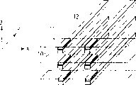
图21表示本发明第1实施例的磁随机存取存储器的单元阵列部分的布局。FIG. 21 shows the layout of the cell array portion of the magnetic random access memory according to the first embodiment of the present invention.
在半导体衬底上边,把多个MTJ元件10叠置成多层(本例中,为3层)。并且,各层中,MTJ元件10在X-Y平面内构成阵列。On the semiconductor substrate, a plurality of
上部线11起读出线功能,沿X方向延伸。上部线11,例如,接触MTJ元件10的自由层。下部线12起读出线和写入线功能,沿Y方向延伸。下部线12,例如,接触MTJ元件10的固定层。并且,例如,上部线11的一端,连接有选择晶体管,下部线12的一端,连接有读出放大器(S/A)。The
写入线13沿Z轴方向延伸,并配置在Z轴方向叠置的多个MTJ元件10的近旁。向MTJ元件10写入的数据(自由层的磁化方向),通过由流入下部线12的沿Y轴方向流动的电流发生的磁场和由流入写入线13的沿Z轴方向流动的电流发生的磁场的合成磁场来决定。The
写入线13的衬底侧一端,连接有选择晶体管(例如,MOS晶体管)14。该选择晶体管14配置在MTJ元件10的阵列正下方。A select transistor (for example, a MOS transistor) 14 is connected to one end of the
按照这种器件构造,在Z轴方向,延伸使用于数据写入/读出的多条导线之中的至少1条(本例中,为写入线13)。According to this device structure, at least one of the plurality of wires for data writing/reading (in this example, the writing line 13 ) is extended in the Z-axis direction.
例如,如果打算使用3条导线实行写入/读出的场合,以往,因为该3条导线全都是沿X轴方向或Y轴方向延伸,所以MTJ元件阵列的每1层,需要至少3此多层布线工艺。对此,本发明例中,关于Z轴方向延伸的导线,可用接触工艺形成,因而可以减少MTJ元件阵列每1层的多层布线工艺次数。For example, if it is intended to use three wires for writing/reading, conventionally, since the three wires all extend in the X-axis direction or the Y-axis direction, at least three wires are required for each layer of the MTJ element array. layer wiring process. In contrast, in the example of the present invention, the conductive wires extending in the Z-axis direction can be formed by a contact process, so that the number of multilayer wiring processes per layer of the MTJ element array can be reduced.
因此,即使增加MTJ元件的叠置数,也能实现提高底膜的平整度和提高MTJ元件的特性。Therefore, even if the number of stacked MTJ elements is increased, improvement of the flatness of the base film and improvement of the characteristics of the MTJ elements can be achieved.
并且,要是三维配置数据写入/读出中所用的导线的话,阵列内线的布局自由度就增加。Furthermore, if the wires used for writing/reading data are arranged three-dimensionally, the degree of freedom in the layout of the wires in the array increases.
例如,如果打算使用3条线实行写入/读出的场合,以往,就形成在写入专用的导线与MTJ元件之间配置读出线的构造,写入专用导线与MTJ元件的距离加大了。对此,本发明例中,例如,采用在Z轴方向延伸写入专用导线的办法,可在MTJ元件近旁配置该写入专用导线,能够抑制加到MTJ元件上的磁场离散。For example, if it is intended to use three lines for writing/reading, conventionally, a structure is formed in which a readout line is arranged between a writing line and the MTJ element, and the distance between the writing line and the MTJ element is increased. up. In this regard, in the example of the present invention, for example, by extending the write-only wire in the Z-axis direction, the write-only wire can be arranged near the MTJ element, and the dispersion of the magnetic field applied to the MTJ element can be suppressed.
进而,关于沿Z轴方向延伸的写入线,其一端应该存在于MTJ元件阵列的下方。所以,很容易在阵列正下方形成连到该导线的晶体管,能够缓和在阵列外围部分密集晶体管。Furthermore, one end of the write line extending in the Z-axis direction should exist below the MTJ element array. Therefore, it is easy to form the transistors connected to the wires directly under the array, and it is possible to relieve the density of transistors in the periphery of the array.
另外,本实施例中,MTJ元件阵列内配置三种类型的导线,各导线互相垂直,而且,制成互相沿不同的方向延伸这样的器件构造。这样,就可以在衬底上边分散配置与各导线连接的晶体管。In addition, in this embodiment, three types of wires are arranged in the MTJ element array, each wire is perpendicular to each other, and a device structure is formed in which the wires extend in different directions from each other. In this way, the transistors connected to the wires can be scattered and arranged on the substrate.
但是,本发明中,Z方向延伸的导线至少有1条就足够,此外的导线多条存在的场合,至于这些导线,无论沿同一方向延伸,或,无论沿不同的方向延伸,也都无妨。However, in the present invention, at least one conducting wire extending in the Z direction is sufficient, and when there are a plurality of other conducting wires, it does not matter whether these conducting wires extend in the same direction or extend in different directions.
②第2实施例②Second embodiment
上述第1实施例中,表示MTJ元件阵列内配置了三种类型导线的场合,然而本发明也可以应用于MTJ元件阵列内,只配置具有起读出/写入线功能的两种导线的场合。In the above-mentioned first embodiment, it is shown that three types of wires are arranged in the MTJ element array, but the present invention can also be applied in the MTJ element array, where only two kinds of wires that have the function of read/write wires are configured. .
图22表示本发明第2实施例的磁随机存取存储器的单元阵列部分的布局。FIG. 22 shows the layout of the cell array portion of the magnetic random access memory according to the second embodiment of the present invention.
在半导体衬底上边,把多个MTJ元件10叠置成多层(本例中,为3层)。并且,各层中,MTJ元件10在X-Y平面内构成阵列。On the semiconductor substrate, a plurality of
MTJ元件10上边,形成导电图形11C。用作写入线和读出线(电流总线)功能的导线13沿Z轴方向延伸,并配置在Z轴方向叠置的多个MTJ元件10近旁。并且,写入线13,连接到Z轴方向叠置的多个MTJ元件10的导电图形11C。On the
导线13的衬底侧一端,连接选择晶体管(例如,MOS晶体管)14。该选择晶体管14配置在MTJ元件10的阵列正下方。One end of the
下部线12用作写入线和读出线(电流总线)功能,沿Y方向延伸。下部线12,例如,与MTJ元件10的固定层接触。并且,例如,下部线12的一端,连接读出放大器(S/A)。The
由MTJ元件10写入的数据(自由层的磁化方向)通过由随流入下部线12沿Y轴方向流动的电流发生的磁场和随流入写入线13里沿Z轴方向流动的电流发生的磁场的合成磁场来决定。The data (magnetization direction of the free layer) written by the
按照这种器件构造,沿Z轴方向延伸使用于数据写入/读出的多条导线之中至少1条(本例中,导线13)。关于Z轴方向延伸的导线,可用接触工艺形成,因而可以减少MTJ元件阵列每1层的多层布线工艺次数。According to this device configuration, at least one of the plurality of wires for data writing/reading is extended in the Z-axis direction (the
本实施例中,MTJ元件阵列的各层中,沿X方向或Y方向延伸的导线只有1条,所以与上述第1实施例比较,进而可以实现提高底膜的平整度,提高MTJ元件的特性。In this embodiment, in each layer of the MTJ element array, there is only one wire extending along the X direction or the Y direction, so compared with the above-mentioned first embodiment, the flatness of the bottom film can be improved, and the characteristics of the MTJ element can be improved. .
并且,采用三维配置数据写入/读出中所用导线的办法,增加阵列内导线布局的自由度,并且,能够抑制给与MTJ元件的磁场的离散。Furthermore, by three-dimensionally arranging the wires used for data writing/reading, the degree of freedom in the layout of the wires in the array is increased, and the dispersion of the magnetic field applied to the MTJ element can be suppressed.
进而,关于Z轴方向延伸的写入线,其一端配置在MTJ元件阵列的正下方。即,通过将与该导线连接的晶体管配置在MTJ元件阵列的正下方,可以缓和阵列外围部分的晶体管密集。Furthermore, one end of the write line extending in the Z-axis direction is arranged directly below the MTJ element array. That is, by arranging the transistors connected to the wires directly below the MTJ element array, the density of transistors in the peripheral portion of the array can be alleviated.
③第3实施例③The third embodiment
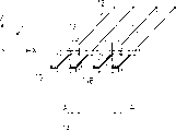
本实施例是上述第1实施例的磁随机存取存储器的变形例。This embodiment is a modified example of the magnetic random access memory of the first embodiment described above.
上述第1实施例中,MTJ元件阵列的1个层内,虽然对1个MTJ元件对应1条写入线,但是本实施例中,在MTJ元件阵列的1个层内,对X方向邻接的2个MTJ元件对应1条写入线。即,在MTJ元件阵列的层内,1条写入线夹入2个MTJ元件中间。In the above-mentioned first embodiment, one write line corresponds to one MTJ element in one layer of the MTJ element array. Two MTJ elements correspond to one write line. That is, in the layer of the MTJ element array, one write line is sandwiched between two MTJ elements.
由于形成这样的构成,可将Z轴方向延伸的写入线条数减少到上述第1实施例中需要条数的一半,正因此,能够实现MTJ元件的高密度。With such a configuration, the number of writing lines extending in the Z-axis direction can be reduced to half of the number required in the first embodiment described above, and because of this, high density of MTJ elements can be realized.
图23表示本发明第3实施例的磁随机存取存储器的单元阵列部分的布局。FIG. 23 shows the layout of the cell array portion of the magnetic random access memory according to the third embodiment of the present invention.
在半导体衬底上边,把多个MTJ10元件叠置成多层(本例中,为3层)。并且,各层中,MTJ元件10在X-Y平面内构成阵列。On the semiconductor substrate, a plurality of MTJ10 elements are stacked in multiple layers (in this example, three layers). Furthermore, in each layer, the
上部线11起读出线功能,沿X方向延伸。上部线11,例如与MTJ元件10的自由层接触。下部线12起读出线和写入线功能,沿Y方向延伸。下部线12,例如接触MTJ元件10的固定层。并且,例如,上部线11的一端,连接选择晶体管,下部线12的一端连接读出放大器(S/A)。The
写入线13沿Z轴方向延伸,配置在Z轴方向叠置的多个MTJ元件10近旁。The
进而,本实施例中,在MTJ元件10的阵列1层内,对X方向邻接的2个MTJ元件对应1条写入线13。即,在MTJ元件阵列的层内,将1条写入线13夹入2个MTJ元件中间。Furthermore, in this embodiment, in one layer of the array of
通过形成这样的构成,可减少Z轴方向延伸的写入线13的条数,正因此,能够实现MTJ元件的高密度。By forming such a configuration, the number of
导线13的衬底侧一端,连接选择晶体管(例如,MOS晶体管)14。该选择晶体管14配置在MTJ元件10的阵列正下方。One end of the
向MTJ元件10写入的数据(自由层的磁化方向)通过由流入下部线12沿Y轴方向流动的电流发生的磁场和由流入写入线13里沿Z轴方向流动的电流发生的磁场的合成磁场来决定。The data written into the MTJ element 10 (magnetization direction of the free layer) passes through the magnetic field generated by the current flowing in the Y-axis direction flowing in the
这里,本实施例中,在写入线13向着一方向流动电流的场合,如图26所示,MTJ元件10的阵列1层内,给予存在于写入线13左侧MTJ元件的磁场方向a1与给与存在于写入线13右侧MTJ元件的磁场方向a2成为互相相反。Here, in this embodiment, when a current flows in one direction through the
于是,对同一写入的动作,存在于写入线13左右的2个MTJ元件磁化状态变成互相不同。Then, for the same writing operation, the magnetization states of the two MTJ elements present on the left and right of the
即,这时,假如存入2个MTJ元件的数据是相同的,就需要使读出存入写入线13左侧MTJ元件的数据时的判定“1”/“0”的条件和读出存入写入线13右侧MTJ元件的数据时的判定“1”/“0”的条件互相相反。That is, at this time, if the data stored in the two MTJ elements is the same, it is necessary to make the condition for judging "1"/"0" and the readout condition when reading the data stored in the MTJ element on the left side of the
按照这种器件构造,沿Z轴方向延伸使用于数据写入/读出的多条导线之中的至少1条(本例中,写入线13)。即,关于沿Z轴方向延伸的导线,因为可用接触工艺形成,所以能够减少MTJ元件阵列每1层的的多层布线工艺次数。According to this device structure, at least one of the plurality of wires for data writing/reading (in this example, the writing wire 13 ) is extended in the Z-axis direction. That is, since the wires extending in the Z-axis direction can be formed by a contact process, the number of multilayer wiring processes per one layer of the MTJ element array can be reduced.
因此,即使增加MTJ元件的叠置数,也能实现提高底膜的平整度和提高MTJ元件的特性。Therefore, even if the number of stacked MTJ elements is increased, improvement of the flatness of the base film and improvement of the characteristics of the MTJ elements can be achieved.
并且,采用三维配置数据写入/读出中所用导线的办法,增加阵列内导线布局的自由度。并且,例如,采用沿Z轴方向延伸写入专用导线的办法,可在MTJ元件近旁配置该写入专用的导线,能够抑制给与MTJ元件的磁场的离散。Furthermore, the method of three-dimensionally arranging the wires used in data writing/reading increases the degree of freedom in the layout of the wires in the array. Furthermore, for example, by extending the write-only lead along the Z-axis direction, the write-only lead can be arranged near the MTJ element, and the dispersion of the magnetic field applied to the MTJ element can be suppressed.
进而,关于Z轴方向延伸的写入线,其一端配置在MTJ元件阵列的正下方。于是,很容易在阵列的正下方配置与该导线连接的晶体管,可以缓和阵列外围部分晶体管密集。Furthermore, one end of the write line extending in the Z-axis direction is arranged directly below the MTJ element array. Therefore, it is easy to arrange the transistors connected to the wire directly under the array, which can ease the density of transistors in the periphery of the array.
并且,本实施例中,MTJ元件阵列的1个层内,对X方向邻接的2个MTJ元件对应1条写入线。即,在MTJ元件阵列的1个层内,将1条写入线夹入2个MTJ元件中间。通过形成这样的构成,可以减少沿Z轴方向延伸的写入线条数,正因此,才能够实现高密度MTJ元件。In addition, in this embodiment, in one layer of the MTJ element array, one write line corresponds to two adjacent MTJ elements in the X direction. That is, in one layer of the MTJ element array, one write line is sandwiched between two MTJ elements. By forming such a structure, the number of writing lines extending in the Z-axis direction can be reduced, and it is precisely because of this that a high-density MTJ element can be realized.
另外,本实施例中,MTJ元件阵列内配置三种类型的导线,各导线互相垂直,而且,形成互相沿不同的方向延伸这样的器件构造。这就是在衬底上分散配置与各导线连接的晶体管的原因。In addition, in this embodiment, three types of wires are arranged in the MTJ element array, each wire is perpendicular to each other, and a device structure is formed in which the wires extend in different directions from each other. This is why the transistors connected to the wires are scattered and arranged on the substrate.
但是,本发明中,Z方向延伸的导线至少有1条就足够,此外的导线存在多条的场合,至于这些导线,无论沿相同方向延伸,或,无论沿不同的方向延伸也都无妨。However, in the present invention, at least one conducting wire extending in the Z direction is sufficient, and when there are a plurality of other conducting wires, it does not matter whether these conducting wires extend in the same direction or extend in different directions.
④第4实施例④ Fourth embodiment
上述第3实施例中,表示MTJ元件阵列内配置了三种类型导线的场合。本实施例中,说明有关MTJ元件的阵列内只配置具有起读出/写入线功能的两种类型导线的磁随机存取存储器。In the above-mentioned third embodiment, the case where three types of wires are arranged in the MTJ element array is shown. In this embodiment, an MRAM in which only two types of wires functioning as read/write lines are arranged in an array of MTJ elements will be described.
图24表示本发明第4实施例的磁随机存取存储器的单元阵列部分的布局。FIG. 24 shows the layout of the cell array portion of the magnetic random access memory according to the fourth embodiment of the present invention.
在半导体衬底上边,把多个MTJ元件10叠置成多层(本例中,为了简单,只示出1层)。并且,各层中,MTJ元件10在X-Y平面内构成阵列。On the semiconductor substrate, a plurality of
MTJ元件10上,形成导电图形11C。用作写入线和读出线(电流总线)功能的导线13沿Z轴方向延伸,并配置在Z轴方向叠置的多个MTJ元件10近旁。并且,写入线13连到Z轴方向叠置的多个MTJ元件10的导电图形11C。On the
进而,本实施例中,MTJ元件10的阵列1个层内,对X方向邻接的2个MTJ元件对应1条写入线13。即,在MTJ元件阵列的1个层内,将条写入线13夹入2个MTJ元件中间。Furthermore, in this embodiment, in one layer of the array of
通过形成这样的构成,可以减少沿Z轴方向延伸的写入线13条数,正因此,才能实现高密度MTJ元件。By forming such a configuration, the number of
导线13的衬底侧一端,连接选择晶体管(例如,MOS晶体管)14。该选择晶体管14配置在MTJ元件10的阵列正下方。One end of the
下部线12起写入线和读出线(电流总线)功能,沿Y方向延伸。下部线12,例如接触MTJ元件10的固定层。并且,例如,下部线12的一端连接读出放大器(S/A)。The
向MTJ元件10写入的数据(自由层的磁化方向)通过由流入下部线12沿Y轴方向流动的电流发生的磁场和由流入写入线13里沿Z轴方向流动的电流发生的磁场的合成磁场来决定。The data written into the MTJ element 10 (magnetization direction of the free layer) passes through the magnetic field generated by the current flowing in the Y-axis direction flowing in the
按照这种器件构造,沿Z轴方向延伸使用于数据写入/读出的多条导线之中至少1条(本例中,导线13)。关于Z轴方向延伸的导线,可用接触工艺形成,因而可以减少MTJ元件阵列每1层的多层布线工艺次数。According to this device configuration, at least one of the plurality of wires for data writing/reading is extended in the Z-axis direction (the
本实施例中,MTJ元件阵列的各层中,沿X方向或Y方向延伸的导线只有1条,所以与上述第3实施例比较,进而,可以实现提高底膜的平整度,提高MTJ元件的特性。In this embodiment, in each layer of the MTJ element array, there is only one conductive wire extending along the X direction or the Y direction, so compared with the above-mentioned third embodiment, further, the flatness of the bottom film can be improved, and the MTJ element can be improved. characteristic.
并且,采用三维配置数据写入/读出中所用导线的办法,增加阵列内导线布局的自由度,并且,能够抑制给与MTJ元件的磁场的离散。Furthermore, by three-dimensionally arranging the wires used for data writing/reading, the degree of freedom in the layout of the wires in the array is increased, and the dispersion of the magnetic field applied to the MTJ element can be suppressed.
进而,关于Z轴方向延伸的写入线,其一端配置在MTJ元件阵列的正下方。即,应该将与该导线连接的晶体管配置在MTJ元件阵列的正下方,可以缓和在阵列外围部分晶体管密集。Furthermore, one end of the write line extending in the Z-axis direction is arranged directly below the MTJ element array. That is, the transistors connected to the wires should be arranged directly under the MTJ element array, so that the density of transistors at the periphery of the array can be alleviated.
并且,本实施例中,MTJ元件阵列的1个层内,对X方向邻接的2个MTJ元件对应1条写入线。即,在MTJ元件阵列的1个层内,将1条写入线夹入2个MTJ元件中间。通过形成这样的构成,可以减少沿Z轴方向延伸的写入线条数,正因此,才能够实现高密度MTJ元件。In addition, in this embodiment, in one layer of the MTJ element array, one write line corresponds to two adjacent MTJ elements in the X direction. That is, in one layer of the MTJ element array, one write line is sandwiched between two MTJ elements. By forming such a structure, the number of writing lines extending in the Z-axis direction can be reduced, and it is precisely because of this that a high-density MTJ element can be realized.
⑤第5实施例⑤ Fifth Embodiment
上述第1到第4实施例中,说明有关沿Z轴方向延伸写入专用导线,或作为读出/写入线功能导线的场合。但是,本发明的特征是,在沿Z轴方向延伸配置于MTJ元件阵列内的多种导线至少1条。In the above-mentioned first to fourth embodiments, the description is made about the case where the write-only wire is extended along the Z-axis direction, or the wire functions as a read/write line. However, the present invention is characterized in that at least one of various kinds of wires is arranged in the MTJ element array extending in the Z-axis direction.
因而,本实施例中,说明有关沿Z轴方向延伸读出专用导线场合的例子。Therefore, in this embodiment, an example in which the read-only wire is extended in the Z-axis direction will be described.
图25表示本发明第5实施例的磁随机存取存储器的单元阵列部分的布局。FIG. 25 shows the layout of the cell array portion of the magnetic random access memory according to the fifth embodiment of the present invention.
在半导体衬底上边,将多个MTJ元件10叠置成多层(本例中,为了简单,只示出1层)。并且,各层中,MTJ元件10在X-Y平面内构成阵列。On the semiconductor substrate, a plurality of
MTJ元件10上边,形成导电图形11C。读出专用线(电流总线)11沿Z轴方向延伸,并配置在Z轴方向叠置的多个MTJ元件10近旁。并且,读出专用线1共同连到Z轴方向叠置的多个MTJ元件10的导电图形11C。On the
进而,本实施例中,MTJ元件10的阵列1个层内,对X方向邻接的2个MTJ元件对应1条读出专用线11。即,在MTJ元件阵列的1个层内,将读出专用线1夹入2个MTJ元件中间。Furthermore, in this embodiment, within one layer of the array of
通过形成这样的构成,可以减少沿Z轴方向延伸的读出专用线条数,正因此,才能实现高密度MTJ元件。By forming such a configuration, the number of read-only lines extending in the Z-axis direction can be reduced, and it is because of this that high-density MTJ elements can be realized.
读出专用线1的衬底侧一端,连接有选择晶体管(例如,MOS晶体管)14。该选择晶体管14被配置在MTJ元件10的阵列的正下方。A selection transistor (for example, a MOS transistor) 14 is connected to one end of the read-
MTJ元件10的上方,配置着与MTJ元件10接近、而不与之接触的写入专用线13。写入专用线13沿X方向延伸。写入专用线13的一端或两端上,连接选择晶体管。Above the
下部线12起读出线和写入线功能,沿Y方向延伸。下部线12,例如接触MTJ元件10的固定层。并且,下部线12的一端,连接读出放大器(S/A)。The
向MTJ元件10写入的数据(自由层的磁化方向)通过由流入下部线12里沿Y轴方向流动的电流发生的磁场和由流入写入线13里沿Z轴方向流动的电流发生的磁场的合成磁场来决定。The data written into the MTJ element 10 (magnetization direction of the free layer) passes through the magnetic field generated by the current flowing in the Y-axis direction flowing in the
按照这种器件构造,沿Z轴方向延伸使用于数据写入/读出的多条导线之中至少1条(本例中,读出专用线11)。即,关于Z轴方向延伸的线,可用接触工艺形成,因而可以减少MTJ元件阵列每1层的多层布线工艺次数。According to this device structure, at least one of the plurality of wires for data writing/reading is extended in the Z-axis direction (in this example, the read-only wire 11). That is, since the lines extending in the Z-axis direction can be formed by a contact process, the number of multilayer wiring processes per layer of the MTJ element array can be reduced.
因此,即使增加MTJ元件的叠置数,也能实现提高底膜的平整度,提高MTJ元件的特性。Therefore, even if the number of stacked MTJ elements is increased, the flatness of the base film can be improved, and the characteristics of the MTJ elements can be improved.
并且,采用三维配置数据写入/读出中所用导线的办法,能够增加阵列内导线布局的自由度。并且,例如,采用沿Z轴方向延伸读出专用导线的办法,可以在MTJ元件的正上方或近旁配置沿X方向延伸的专用导线,能够抑制给与MTJ元件的磁场的离散。Furthermore, by three-dimensionally arranging the wires used in data writing/reading, the degree of freedom in the layout of the wires in the array can be increased. Furthermore, for example, by extending the readout dedicated wire along the Z-axis direction, the dedicated wire extending along the X direction can be arranged directly above or near the MTJ element, thereby suppressing the dispersion of the magnetic field applied to the MTJ element.
进而,关于Z轴方向延伸的专用线,其一端就存在MTJ元件阵列的正下方。于是,很容易在阵列的正下方,形成与该导线连接的晶体管,可以缓和在阵列外围部分晶体管密集。Furthermore, one end of the dedicated line extending in the Z-axis direction exists directly below the MTJ element array. Therefore, it is easy to form transistors connected to the wire directly under the array, and the density of transistors in the periphery of the array can be eased.
并且,本实施例中,MTJ元件阵列的1个层内,对X方向邻接的2个MTJ元件对应1条写入线。即,在MTJ元件阵列的1个层内,将1条专用线夹入2个MTJ元件中间。通过形成这样的构成,可以减少沿Z轴方向延伸的专用线条数,正因此,才能够实现高密度MTJ元件。In addition, in this embodiment, in one layer of the MTJ element array, one write line corresponds to two adjacent MTJ elements in the X direction. That is, in one layer of the MTJ element array, one dedicated line is sandwiched between two MTJ elements. By forming such a configuration, the number of dedicated lines extending in the Z-axis direction can be reduced, and it is because of this that high-density MTJ elements can be realized.
⑥第6实施例⑥The sixth embodiment
图27表示本发明第6实施例的磁随机存取存储器的单元阵列部分的布局。FIG. 27 shows the layout of the cell array portion of the magnetic random access memory according to the sixth embodiment of the present invention.
在半导体衬底上边,将多个MTJ元件10叠置成多层(本例中,为3层)。并且,各层中,MTJ元件10在X-Y平面内构成阵列。On the semiconductor substrate, a plurality of
上部线11起读出线功能,沿X方向延伸。上部线11,例如,与MTJ元件10的自由层接触。下部线12起读出线和写入线功能,沿Y方向延伸。下部线12,例如,接触MTJ元件10的固定层。并且,例如,上部线11的一端,连接选择晶体管,下部线12的一端连接读出放大器(S/A)。The
写入线13沿Z轴方向延伸,配置在Z轴方向叠置的多个MTJ元件10近旁。向MTJ元件10写入的数据(自由层的磁化方向)通过由流入下部线12里沿Y轴方向流动的电流发生的磁场和由流入写入线13里沿Z轴方向流动的电流发生的磁场的合成磁场来决定。The
至少2条写入线13互相串联连接起来。串联连接的写入线13一端或另一端上,分别连接选择晶体管14(例如,MOS晶体管)。该选择晶体管14被配置在MTJ元件10的阵列的正下方。At least two write
即使这种器件构造,数据的写入/读出中所用的多条导线中,至少1条(本例中,写入线13)沿Z轴方向延伸。因此,也能获得与第1实施例同样的效果,例如,即使增加MTJ元件的叠置数,也能实现提高底膜的平整度,提高MTJ元件特性的这种效果。Even with such a device structure, at least one of the plurality of wires used for writing/reading data (in this example, the writing wire 13 ) extends in the Z-axis direction. Therefore, the same effects as those of the first embodiment can be obtained. For example, even if the number of stacked MTJ elements is increased, the flatness of the base film can be improved and the characteristics of the MTJ elements can be improved.
⑦第7实施例⑦ Seventh embodiment
上述第1到第6实施例中,沿Z轴方向延伸的导线,可用接触工艺来形成。但是,如果MTJ元件的叠置数非常多的话,就难以用1次蚀刻工序形成接触孔。In the above-mentioned first to sixth embodiments, the conductive wires extending along the Z-axis direction can be formed by a contact process. However, if the number of stacked MTJ elements is very large, it is difficult to form contact holes in one etching process.
因而,本实施例中,提出一种不仅一次形成沿Z轴方向延伸的导线,而且分成多次形成导线的技术。Therefore, in the present embodiment, a technique of not only forming the conductive lines extending in the Z-axis direction at one time but also forming the conductive lines in multiple times is proposed.
图28中,关于多层叠置MTJ元件的阵列构造,提出在每1层形成MTJ元件和沿X方向和Y方向延伸的导线,同时也形成沿Z轴方向延伸的导线。这时,沿Z轴方向延伸的导线,由多个部分1-1、1-2、1-3、1-4的集合构成。In FIG. 28 , regarding the array structure of multilayer stacked MTJ elements, it is proposed to form MTJ elements and wires extending in the X and Y directions for each layer, and also form wires extending in the Z-axis direction. At this time, the conducting wire extending in the Z-axis direction is constituted by a collection of a plurality of parts 1-1, 1-2, 1-3, and 1-4.
图29的例子是改进图28的例子。The example of FIG. 29 is an improvement of the example of FIG. 28 .
图28的例子中,沿Z轴方向延伸的导线各部分1-1、1-2、1-3、1-4中发生对准偏移的场合,发生断线、线电阻增大等问题。因而,在图29例子中,关于多层叠置的MTJ元件的阵列构造,在每1层形成沿Z轴方向延伸的导线,同时考虑其上对准的偏移,形成中间层2-1、2-2、2-3。因此,即使在沿Z轴方向延伸的导线各部分1-1、1-2、1-3、1-4中发生对准偏移,也不会发生断线、线电阻增大等问题。In the example of FIG. 28, when the misalignment occurs in the lead wire portions 1-1, 1-2, 1-3, and 1-4 extending in the Z-axis direction, problems such as disconnection and increase in wire resistance occur. Therefore, in the example of FIG. 29 , regarding the array structure of MTJ elements stacked in multiple layers, conductive lines extending in the Z-axis direction are formed for each layer, and intermediate layers 2-1, 2 are formed taking into account the misalignment of alignment thereon. -2, 2-3. Therefore, even if misalignment occurs in each of the wire portions 1-1, 1-2, 1-3, 1-4 extending in the Z-axis direction, problems such as disconnection and increase in wire resistance do not occur.
(4)其它(4) Others
上述第1到第6实施例中,与MTJ元件阵列内的线连接的晶体管,一般的是MOS晶体管,但也可以是双极晶体管、二极管等。In the above-mentioned first to sixth embodiments, the transistors connected to the lines in the MTJ element array are generally MOS transistors, but may be bipolar transistors, diodes, and the like.
本发明只要是具有多层叠置MTJ元件的单元阵列构造的磁随机存取存储器,不管构造也能应用。The present invention can be applied regardless of the structure as long as it is a magnetic random access memory having a cell array structure of stacked MTJ elements.
(5)结束语(5) Conclusion
以上,如说明的那样,按照本发明例的磁随机存取存储器,在纵向(MTJ元件叠置的方向),使MTJ元件阵列内配置的多种线之中的至少1条线延伸。As described above, according to the magnetic random access memory of the example of the present invention, at least one of the various lines arranged in the MTJ element array is extended in the longitudinal direction (the direction in which the MTJ elements are stacked).
其结果,可以减少横向延伸的线数,就能防止底膜平整度的恶化,抑制MTJ元件特性恶化。并且,提高阵列内的布局自由度,缩小给与MTJ元件的磁场的离散。进而,因为现在已经可以在阵列下方配置晶体管,所以能够缓和在阵列外围分晶体管密集。As a result, the number of lines stretched in the lateral direction can be reduced, the deterioration of the flatness of the base film can be prevented, and the deterioration of the characteristics of the MTJ element can be suppressed. Furthermore, the degree of freedom of layout in the array is improved, and the dispersion of the magnetic field applied to the MTJ elements is reduced. Furthermore, since transistors can already be arranged below the array, it is possible to reduce the density of transistors on the periphery of the array.
其它的优点和改进对本领域普通技术人员是显而易见的。因此,本发明概括起来说,并不限于这里表示和描述的具体细节和表现的各实施例。所以,在不脱离由附属权利要求书及其等同物所限定的本发明总构思的精神或范围的前提下,可以作各种各样的修改。Additional advantages and modifications will readily appear to those skilled in the art. Therefore, the invention in general is not limited to the specific details and representative embodiments shown and described herein. Accordingly, various modifications may be made without departing from the spirit or scope of the general inventive concept as defined by the appended claims and their equivalents.
Claims (67)
Applications Claiming Priority (6)
| Application Number | Priority Date | Filing Date | Title |
|---|---|---|---|
| JP2001367755A JP4068337B2 (en) | 2001-11-30 | 2001-11-30 | Magnetic random access memory |
| JP367941/2001 | 2001-11-30 | ||
| JP367754/2001 | 2001-11-30 | ||
| JP2001367754A JP2003168785A (en) | 2001-11-30 | 2001-11-30 | Magnetic random access memory |
| JP2001367941A JP4091298B2 (en) | 2001-11-30 | 2001-11-30 | Magnetic random access memory |
| JP367755/2001 | 2001-11-30 |
Related Child Applications (1)
| Application Number | Title | Priority Date | Filing Date |
|---|---|---|---|
| CN200510118783.4A Division CN1783337B (en) | 2001-11-30 | 2002-11-29 | Magnetic random access memory |
Publications (2)
| Publication Number | Publication Date |
|---|---|
| CN1431663A true CN1431663A (en) | 2003-07-23 |
| CN100358047C CN100358047C (en) | 2007-12-26 |
Family
ID=27347895
Family Applications (1)
| Application Number | Title | Priority Date | Filing Date |
|---|---|---|---|
| CNB021518491A Expired - Fee Related CN100358047C (en) | 2001-11-30 | 2002-11-29 | magnetic random access memory |
Country Status (4)
| Country | Link |
|---|---|
| US (3) | US6807086B2 (en) |
| KR (1) | KR100537116B1 (en) |
| CN (1) | CN100358047C (en) |
| TW (1) | TW582032B (en) |
Cited By (3)
| Publication number | Priority date | Publication date | Assignee | Title |
|---|---|---|---|---|
| CN100452233C (en) * | 2005-01-28 | 2009-01-14 | 株式会社东芝 | Spin injection magnetic random access memory and writing method |
| CN110910924A (en) * | 2018-09-18 | 2020-03-24 | 联华电子股份有限公司 | Magnetoresistive random access memory |
| CN115315748A (en) * | 2020-03-27 | 2022-11-08 | 华为技术有限公司 | Magnetic random access memory and electronic equipment |
Families Citing this family (28)
| Publication number | Priority date | Publication date | Assignee | Title |
|---|---|---|---|---|
| JP3906067B2 (en) * | 2001-11-30 | 2007-04-18 | 株式会社東芝 | Magnetic random access memory |
| US7042749B2 (en) * | 2002-05-16 | 2006-05-09 | Micron Technology, Inc. | Stacked 1T-nmemory cell structure |
| WO2003098636A2 (en) * | 2002-05-16 | 2003-11-27 | Micron Technology, Inc. | STACKED 1T-nMEMORY CELL STRUCTURE |
| US6940748B2 (en) * | 2002-05-16 | 2005-09-06 | Micron Technology, Inc. | Stacked 1T-nMTJ MRAM structure |
| JP4646485B2 (en) * | 2002-06-25 | 2011-03-09 | ルネサスエレクトロニクス株式会社 | Thin film magnetic memory device |
| US6925003B2 (en) * | 2003-09-08 | 2005-08-02 | Hewlett-Packard Development Company, L.P. | Magnetic memory cell structure |
| US6847544B1 (en) * | 2003-10-20 | 2005-01-25 | Hewlett-Packard Development Company, L.P. | Magnetic memory which detects changes between first and second resistive states of memory cell |
| US7102921B2 (en) * | 2004-05-11 | 2006-09-05 | Hewlett-Packard Development Company, L.P. | Magnetic memory device |
| US7061037B2 (en) * | 2004-07-06 | 2006-06-13 | Maglabs, Inc. | Magnetic random access memory with multiple memory layers and improved memory cell selectivity |
| JP2006344281A (en) * | 2005-06-08 | 2006-12-21 | Toshiba Corp | Magnetic random access memory |
| EA014460B1 (en) * | 2005-10-21 | 2010-12-30 | Наталия Орденес Ааг | Dismantlable shoe |
| US7426133B2 (en) * | 2005-10-24 | 2008-09-16 | Honeywell International, Inc. | Complementary giant magneto-resistive memory with full-turn word line |
| US8120949B2 (en) * | 2006-04-27 | 2012-02-21 | Avalanche Technology, Inc. | Low-cost non-volatile flash-RAM memory |
| US8199576B2 (en) * | 2009-04-08 | 2012-06-12 | Sandisk 3D Llc | Three-dimensional array of re-programmable non-volatile memory elements having vertical bit lines and a double-global-bit-line architecture |
| US8351236B2 (en) * | 2009-04-08 | 2013-01-08 | Sandisk 3D Llc | Three-dimensional array of re-programmable non-volatile memory elements having vertical bit lines and a single-sided word line architecture |
| KR101793286B1 (en) * | 2009-04-08 | 2017-11-02 | 샌디스크 테크놀로지스 엘엘씨 | Three-dimensional array of re-programmable nonvolatile memory elements having vertical bit lines and a single-sided word line architecture |
| US7983065B2 (en) * | 2009-04-08 | 2011-07-19 | Sandisk 3D Llc | Three-dimensional array of re-programmable non-volatile memory elements having vertical bit lines |
| US8526237B2 (en) | 2010-06-08 | 2013-09-03 | Sandisk 3D Llc | Non-volatile memory having 3D array of read/write elements and read/write circuits and method thereof |
| US20110297912A1 (en) * | 2010-06-08 | 2011-12-08 | George Samachisa | Non-Volatile Memory Having 3d Array of Read/Write Elements with Vertical Bit Lines and Laterally Aligned Active Elements and Methods Thereof |
| JP5686698B2 (en) * | 2011-08-05 | 2015-03-18 | ルネサスエレクトロニクス株式会社 | Semiconductor device |
| JP2013041912A (en) * | 2011-08-12 | 2013-02-28 | Toshiba Corp | Magnetic random access memory |
| WO2013095540A1 (en) * | 2011-12-22 | 2013-06-27 | Intel Corporation | Memory with elements having two stacked magnetic tunneling junction (mtj) devices |
| EP2688103A1 (en) * | 2012-07-20 | 2014-01-22 | Crocus Technology S.A. | MRAM cell and device with improved field line for reduced power consumption |
| US9299917B2 (en) * | 2013-09-30 | 2016-03-29 | Northwestern University | Magnetic tunnel junctions with control wire |
| KR102477093B1 (en) | 2015-10-13 | 2022-12-13 | 삼성전자주식회사 | Apparatus and Method for performing Fourier transform |
| JP6477752B2 (en) * | 2017-03-13 | 2019-03-06 | Tdk株式会社 | Magnetic sensor |
| US10262715B2 (en) | 2017-03-27 | 2019-04-16 | Micron Technology, Inc. | Multiple plate line architecture for multideck memory array |
| KR102684719B1 (en) * | 2020-05-14 | 2024-07-12 | 삼성전자주식회사 | Memory device and method of manufacturing the same |
Family Cites Families (35)
| Publication number | Priority date | Publication date | Assignee | Title |
|---|---|---|---|---|
| US4791604A (en) * | 1984-02-15 | 1988-12-13 | Joseph J. Bednarz | Sheet random access memory |
| US6590750B2 (en) * | 1996-03-18 | 2003-07-08 | International Business Machines Corporation | Limiting magnetoresistive electrical interaction to a preferred portion of a magnetic region in magnetic devices |
| JP3392657B2 (en) | 1996-09-26 | 2003-03-31 | 株式会社東芝 | Semiconductor storage device |
| JP3132437B2 (en) * | 1997-09-26 | 2001-02-05 | 日本電気株式会社 | Semiconductor storage device |
| US5991193A (en) * | 1997-12-02 | 1999-11-23 | International Business Machines Corporation | Voltage biasing for magnetic ram with magnetic tunnel memory cells |
| JP2000076844A (en) | 1998-05-18 | 2000-03-14 | Canon Inc | Magnetic thin film memory element, recording / reproducing method thereof, and image recording / reproducing apparatus |
| EP0959475A3 (en) * | 1998-05-18 | 2000-11-08 | Canon Kabushiki Kaisha | Magnetic thin film memory and recording and reproducing method and apparatus using such a memory |
| JP2000187976A (en) | 1998-12-17 | 2000-07-04 | Canon Inc | Magnetic thin film memory and recording / reproducing method thereof |
| US5969978A (en) | 1998-09-30 | 1999-10-19 | The United States Of America As Represented By The Secretary Of The Navy | Read/write memory architecture employing closed ring elements |
| JP2000195250A (en) | 1998-12-24 | 2000-07-14 | Toshiba Corp | Magnetic memory device |
| JP2001067862A (en) | 1999-09-01 | 2001-03-16 | Sanyo Electric Co Ltd | Magnetic memory element |
| US6166948A (en) * | 1999-09-03 | 2000-12-26 | International Business Machines Corporation | Magnetic memory array with magnetic tunnel junction memory cells having flux-closed free layers |
| JP2001084758A (en) * | 1999-09-17 | 2001-03-30 | Fujitsu Ltd | Ferromagnetic tunnel junction random access memory, spin valve random access memory, single ferromagnetic film random access memory, and memory cell array using them |
| JP3913971B2 (en) | 1999-12-16 | 2007-05-09 | 株式会社東芝 | Magnetic memory device |
| JP3758933B2 (en) | 2000-03-27 | 2006-03-22 | シャープ株式会社 | Magnetic memory and recording method thereof |
| US6172904B1 (en) * | 2000-01-27 | 2001-01-09 | Hewlett-Packard Company | Magnetic memory cell with symmetric switching characteristics |
| JP2001217398A (en) | 2000-02-03 | 2001-08-10 | Rohm Co Ltd | Storage device using ferromagnetic tunnel junction element |
| DE10015193A1 (en) | 2000-03-27 | 2001-10-25 | Infineon Technologies Ag | Highly integrated system-on-chip systems with non-volatile memory units |
| US6515897B1 (en) * | 2000-04-13 | 2003-02-04 | International Business Machines Corporation | Magnetic random access memory using a non-linear memory element select mechanism |
| JP2002025245A (en) | 2000-06-30 | 2002-01-25 | Nec Corp | Nonvolatile semiconductor storage device and information recording method |
| US6456525B1 (en) * | 2000-09-15 | 2002-09-24 | Hewlett-Packard Company | Short-tolerant resistive cross point array |
| JP4149647B2 (en) * | 2000-09-28 | 2008-09-10 | 株式会社東芝 | Semiconductor memory device and manufacturing method thereof |
| DE10053965A1 (en) * | 2000-10-31 | 2002-06-20 | Infineon Technologies Ag | Method for preventing unwanted programming in an MRAM arrangement |
| DE10054520C1 (en) | 2000-11-03 | 2002-03-21 | Infineon Technologies Ag | Data memory with several databanks has respective column control devices for different databanks arranged in common plane extending in row direction |
| JP4667594B2 (en) * | 2000-12-25 | 2011-04-13 | ルネサスエレクトロニクス株式会社 | Thin film magnetic memory device |
| US6522579B2 (en) * | 2001-01-24 | 2003-02-18 | Infineon Technologies, Ag | Non-orthogonal MRAM device |
| JP2002359355A (en) | 2001-05-28 | 2002-12-13 | Internatl Business Mach Corp <Ibm> | Nonvolatile magnetic memory cell having multilayer structure and storage circuit block using the same |
| JP2003016777A (en) * | 2001-06-28 | 2003-01-17 | Mitsubishi Electric Corp | Thin film magnetic storage device |
| JP2003133528A (en) | 2001-10-24 | 2003-05-09 | Sony Corp | Information storage device, information writing method thereof and manufacturing method thereof |
| US6795334B2 (en) * | 2001-12-21 | 2004-09-21 | Kabushiki Kaisha Toshiba | Magnetic random access memory |
| DE10202903B4 (en) * | 2002-01-25 | 2009-01-22 | Qimonda Ag | Magnetoresistive memory cell with polarity-dependent resistor and memory cell |
| JP3875568B2 (en) * | 2002-02-05 | 2007-01-31 | 株式会社東芝 | Semiconductor device and manufacturing method thereof |
| JP3959335B2 (en) * | 2002-07-30 | 2007-08-15 | 株式会社東芝 | Magnetic storage device and manufacturing method thereof |
| JP2004146687A (en) * | 2002-10-25 | 2004-05-20 | Toshiba Corp | Magnetic storage device and method of manufacturing the same |
| US6859410B2 (en) * | 2002-11-27 | 2005-02-22 | Matrix Semiconductor, Inc. | Tree decoder structure particularly well-suited to interfacing array lines having extremely small layout pitch |
-
2002
- 2002-11-29 TW TW091134785A patent/TW582032B/en not_active IP Right Cessation
- 2002-11-29 US US10/305,988 patent/US6807086B2/en not_active Expired - Fee Related
- 2002-11-29 CN CNB021518491A patent/CN100358047C/en not_active Expired - Fee Related
- 2002-11-30 KR KR10-2002-0075649A patent/KR100537116B1/en not_active Expired - Fee Related
-
2004
- 2004-09-09 US US10/936,693 patent/US7151691B2/en not_active Expired - Fee Related
-
2006
- 2006-07-10 US US11/482,817 patent/US7405962B2/en not_active Expired - Fee Related
Cited By (3)
| Publication number | Priority date | Publication date | Assignee | Title |
|---|---|---|---|---|
| CN100452233C (en) * | 2005-01-28 | 2009-01-14 | 株式会社东芝 | Spin injection magnetic random access memory and writing method |
| CN110910924A (en) * | 2018-09-18 | 2020-03-24 | 联华电子股份有限公司 | Magnetoresistive random access memory |
| CN115315748A (en) * | 2020-03-27 | 2022-11-08 | 华为技术有限公司 | Magnetic random access memory and electronic equipment |
Also Published As
| Publication number | Publication date |
|---|---|
| US6807086B2 (en) | 2004-10-19 |
| KR100537116B1 (en) | 2005-12-16 |
| US7405962B2 (en) | 2008-07-29 |
| US7151691B2 (en) | 2006-12-19 |
| CN100358047C (en) | 2007-12-26 |
| US20060262595A1 (en) | 2006-11-23 |
| TW582032B (en) | 2004-04-01 |
| US20030103377A1 (en) | 2003-06-05 |
| TW200304140A (en) | 2003-09-16 |
| KR20030044891A (en) | 2003-06-09 |
| US20050030813A1 (en) | 2005-02-10 |
Similar Documents
| Publication | Publication Date | Title |
|---|---|---|
| CN1431663A (en) | magnetic random access memory | |
| CN1269134C (en) | Magnetic random access memory and mfg. method thereof | |
| CN1263040C (en) | Film magnetic storing device for writing data by magetic field exerting | |
| CN1294596C (en) | Magnetic random access memory and readout method and mfg. method | |
| CN1286115C (en) | Magnetic random access storage device and its read-out circuit and producing method thereof | |
| CN1213435C (en) | A storage device with a large data readout tolerance that stores data by utilizing changes in resistance value | |
| CN1231917C (en) | Thin film magnet memory able to stable read out datas and write in datas | |
| CN1210718C (en) | Film magnetic body storage possessing highly integrated storage array | |
| CN1490818A (en) | Thin film magnetic memory and related semiconductor integrated circuit devices | |
| CN1310253C (en) | Magnetic random access memory and mfg. method thereof | |
| CN1497602A (en) | magnetic random access memory | |
| CN1295707C (en) | Magnetic storage device with magnetic shielding layer and mfg. method thereof | |
| CN1448944A (en) | Film magnetic storage device equipped with false elements for data reading reference | |
| CN1349226A (en) | Thin film magnet storage device for writing easy-control data into current | |
| CN1305140C (en) | Magnetic RAM and its data reading method | |
| CN1172374C (en) | semiconductor memory | |
| CN1610001A (en) | Semiconductor memory device with magnetoresistance elements and method of writing data into the same | |
| CN1811984A (en) | Spin-injection magnetic random access memory and write-in method | |
| CN1469386A (en) | magnetic random access memory | |
| CN1956207A (en) | Spin-injection magnetic random access memory | |
| CN1448943A (en) | magnetic storage device | |
| CN1442859A (en) | Magnetic random access storage device | |
| CN1707689A (en) | Magnetic random access memory | |
| CN1505038A (en) | Storage apparatus capable of prolixity displacement and high-speed reading-out | |
| CN1941449A (en) | Magneto-resistive element, method for manufacturing the same and magnetic random access memory |
Legal Events
| Date | Code | Title | Description |
|---|---|---|---|
| C06 | Publication | ||
| PB01 | Publication | ||
| C10 | Entry into substantive examination | ||
| SE01 | Entry into force of request for substantive examination | ||
| C14 | Grant of patent or utility model | ||
| GR01 | Patent grant | ||
| C17 | Cessation of patent right | ||
| CF01 | Termination of patent right due to non-payment of annual fee |
Granted publication date: 20071226 Termination date: 20121129 |