CN1400696A - Manufacture of electrical contact - Google Patents
Manufacture of electrical contact Download PDFInfo
- Publication number
- CN1400696A CN1400696A CN02127068A CN02127068A CN1400696A CN 1400696 A CN1400696 A CN 1400696A CN 02127068 A CN02127068 A CN 02127068A CN 02127068 A CN02127068 A CN 02127068A CN 1400696 A CN1400696 A CN 1400696A
- Authority
- CN
- China
- Prior art keywords
- metallic plate
- mask layer
- contact
- microstar
- etched
- Prior art date
- Legal status (The legal status is an assumption and is not a legal conclusion. Google has not performed a legal analysis and makes no representation as to the accuracy of the status listed.)
- Pending
Links
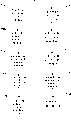
Images


Classifications
-
- H—ELECTRICITY
- H01—ELECTRIC ELEMENTS
- H01R—ELECTRICALLY-CONDUCTIVE CONNECTIONS; STRUCTURAL ASSOCIATIONS OF A PLURALITY OF MUTUALLY-INSULATED ELECTRICAL CONNECTING ELEMENTS; COUPLING DEVICES; CURRENT COLLECTORS
- H01R12/00—Structural associations of a plurality of mutually-insulated electrical connecting elements, specially adapted for printed circuits, e.g. printed circuit boards [PCB], flat or ribbon cables, or like generally planar structures, e.g. terminal strips, terminal blocks; Coupling devices specially adapted for printed circuits, flat or ribbon cables, or like generally planar structures; Terminals specially adapted for contact with, or insertion into, printed circuits, flat or ribbon cables, or like generally planar structures
- H01R12/50—Fixed connections
- H01R12/51—Fixed connections for rigid printed circuits or like structures
- H01R12/55—Fixed connections for rigid printed circuits or like structures characterised by the terminals
- H01R12/57—Fixed connections for rigid printed circuits or like structures characterised by the terminals surface mounting terminals
-
- H—ELECTRICITY
- H01—ELECTRIC ELEMENTS
- H01R—ELECTRICALLY-CONDUCTIVE CONNECTIONS; STRUCTURAL ASSOCIATIONS OF A PLURALITY OF MUTUALLY-INSULATED ELECTRICAL CONNECTING ELEMENTS; COUPLING DEVICES; CURRENT COLLECTORS
- H01R13/00—Details of coupling devices of the kinds covered by groups H01R12/70 or H01R24/00 - H01R33/00
- H01R13/02—Contact members
- H01R13/22—Contacts for co-operating by abutting
- H01R13/24—Contacts for co-operating by abutting resilient; resiliently-mounted
- H01R13/2407—Contacts for co-operating by abutting resilient; resiliently-mounted characterized by the resilient means
-
- H—ELECTRICITY
- H05—ELECTRIC TECHNIQUES NOT OTHERWISE PROVIDED FOR
- H05K—PRINTED CIRCUITS; CASINGS OR CONSTRUCTIONAL DETAILS OF ELECTRIC APPARATUS; MANUFACTURE OF ASSEMBLAGES OF ELECTRICAL COMPONENTS
- H05K3/00—Apparatus or processes for manufacturing printed circuits
- H05K3/40—Forming printed elements for providing electric connections to or between printed circuits
- H05K3/4007—Surface contacts, e.g. bumps
- H05K3/4015—Surface contacts, e.g. bumps using auxiliary conductive elements, e.g. pieces of metal foil, metallic spheres
-
- H—ELECTRICITY
- H01—ELECTRIC ELEMENTS
- H01L—SEMICONDUCTOR DEVICES NOT COVERED BY CLASS H10
- H01L2924/00—Indexing scheme for arrangements or methods for connecting or disconnecting semiconductor or solid-state bodies as covered by H01L24/00
- H01L2924/0001—Technical content checked by a classifier
- H01L2924/0002—Not covered by any one of groups H01L24/00, H01L24/00 and H01L2224/00
-
- H—ELECTRICITY
- H01—ELECTRIC ELEMENTS
- H01R—ELECTRICALLY-CONDUCTIVE CONNECTIONS; STRUCTURAL ASSOCIATIONS OF A PLURALITY OF MUTUALLY-INSULATED ELECTRICAL CONNECTING ELEMENTS; COUPLING DEVICES; CURRENT COLLECTORS
- H01R12/00—Structural associations of a plurality of mutually-insulated electrical connecting elements, specially adapted for printed circuits, e.g. printed circuit boards [PCB], flat or ribbon cables, or like generally planar structures, e.g. terminal strips, terminal blocks; Coupling devices specially adapted for printed circuits, flat or ribbon cables, or like generally planar structures; Terminals specially adapted for contact with, or insertion into, printed circuits, flat or ribbon cables, or like generally planar structures
- H01R12/70—Coupling devices
- H01R12/71—Coupling devices for rigid printing circuits or like structures
- H01R12/712—Coupling devices for rigid printing circuits or like structures co-operating with the surface of the printed circuit or with a coupling device exclusively provided on the surface of the printed circuit
- H01R12/714—Coupling devices for rigid printing circuits or like structures co-operating with the surface of the printed circuit or with a coupling device exclusively provided on the surface of the printed circuit with contacts abutting directly the printed circuit; Button contacts therefore provided on the printed circuit
Abstract
The present invention relates to a method for the fabrication of electrical contacts using metal forming, masking, etching, and soldering techniques is presented. The method produces a plurality of specialized electrical contacts, capable of use in an interposer, or other device, including non-permanent or permanent electrical connections providing contact wipe, soft spring rates, durability, and significant amounts of travel.
Description
Technical field
The present invention relates generally to the electric contact field, more specifically relates to the manufacture method of electric contact.
Background of invention
Existing electric contact design comprises inserter that is made of elastomeric material and the inserter that is made of wire ball.All there is intrinsic limitation in these two kinds of technical schemes at design aspect.Current elastomeric material can not kept enough contacting elastic force and have little working height scope after after a while with under surpassing the situation of uniform temperature.The inserter that is made of wire ball is frangible, gets loose easily, often needs expensive inspection, and the contact travel that is provided is limited.
Summary of the invention
The present invention relates to a kind of method of utilizing metal forming, mask, etching and solder technology to make electric contact.This method can be produced a large amount of special-purpose electric contacts that can be used in inserter or other devices, comprises impermanency or nonvolatil electrical connection, so that contact friction, resilient flexible rigidity, durability and big stroke to be provided.
Show principle of the present invention below in conjunction with specifying of accompanying drawing, can find out other aspects and advantages of the present invention significantly from these detailed descriptions with way of example.
Brief Description Of Drawings
Fig. 1 is the perspective view according to the embodiment of the printed circuit board (PCB) that comprises a plurality of plated-through holes of the present invention.
Fig. 2 is the perspective view that comprises the embodiment of the metallic plate that a plurality of domes swell according to of the present invention.
Fig. 3 is the perspective view of metallic plate shown in the Fig. 2 after plate being formed mask and being etched with a plurality of electric contacts of formation according to the present invention.
Fig. 4 is by the metallic plate shown in Fig. 3 being welded to the perspective view of the formed structure of printed circuit board (PCB) shown in Fig. 1 according to the present invention.
Fig. 5 is the perspective view of the structure among the Fig. 4 after the coupling part between the single electric contact is etched away according to the present invention.
Fig. 6 is the perspective view of the structure among the Fig. 5 after electric contact is by plating according to the present invention.
Fig. 7 is a flow chart of the method for electric contact constructed in accordance.
Fig. 8 is a flow chart of the method for the inserter that comprises the wheeled contact of Microstar constructed in accordance.
Fig. 9 is the flow chart of method of the inserter of a plurality of balls that comprise wheeled contact of Microstar and ball grid array (BGA) constructed in accordance.
Figure 10 is the flow chart of the method for the wheeled contact of Microstar constructed in accordance.
Figure 11 is the perspective view according to the embodiment of the wheeled contact of Microstar with three supporting legs of the present invention.
Figure 12 is the perspective view of the embodiment of the Microstar wheeled contact of a plurality of on substrate according to the present invention with three supporting legs.
Figure 13 is a sectional view according to an embodiment of the invention, and it shows the wheeled contact of Microstar on first side that is arranged on substrate and is arranged on a plurality of balls of the ball grid array (BGA) on second side of substrate.
Embodiment
Fig. 1 is the perspective view according to an embodiment of the printed circuit board (PCB) (PCB) that comprises a plurality of plated-through holes 106 of the present invention.In one embodiment of the invention, be coated with copper on two sides of printed circuit board base board 100, these copper are etched and stay the copper district 104 in each hole 102 on the relative both sides of substrate then.Though the shape in the copper district 104 among this embodiment is ovalize a little, in the scope of the invention, the copper district 104 of other shapes also will play a role equally well.For example, in some embodiments of the invention, copper district 104 can be circle, square, rectangle or other more complicated shapes.Though copper is preferable alloy, other embodiment of the present invention also can use other coating materials.Substrate 100 can comprise multiple material, and the material of selecting is a glass fibre usually.Get out the hole 102 of passing 104 centers, copper district then.The cylinder of following the formation of described hole is metallized, and with the corresponding copper district 104 on the opposite flank that is connected substrate 100, thereby forms plated-through hole array 106.Can form the boring and the PCB of plating by any Standard PC B manufacturing system, and the PCB that described boring and quilt are plated will be as the substrate of a plurality of special-purpose electric contacts, described a plurality of special-purpose electric contacts refer to the wheeled contact of Microstar here.The PCB that has these wheeled contacts of Microstar can be used as the inserter in the electronic system.
Fig. 2 is the perspective view that comprises the embodiment of the metallic plate that a plurality of domes swell according to of the present invention.Metallic plate 200 is processed into and comprises a plurality of little dome protuberances 202.Described metallic plate 200 can be made by copper or other required conducting metals of any specific embodiment of the present invention.The size of dome protuberance 202 also can be that any specific embodiment needs according to the present invention change.In one embodiment of the invention, the dome protuberance 202 in metallic plate 200 is one to one with the plated-through hole 102 on the PCB substrate 100, yet other embodiment of the present invention need not to keep this relation one to one.
Fig. 3 is the perspective view of metallic plate shown in the Fig. 2 after plate 200 being carried out mask and being etched with the wheeled contact of a plurality of Microstars of formation according to the present invention, and wherein the wheeled contact of each Microstar is on the pedestal 304 of himself.At metallic plate 200 masked and be etched with after, stay the coupling part 302 between the wheeled contact 300 of Microstar, pedestal 304 and the single pedestal 304, form one through overetched metallic plate 310.It should be noted, though Fig. 3 shows the regular array of the wheeled contact 300 of Microstar, but need not to make a plurality of Microstars wheeled contact formation rule array, but can only form the wheeled contact of Microstar and can connect the wheeled contact 300 of a plurality of Microstars with longer coupling part 302 in needed position.
Fig. 4 is by the metallic plate shown in Fig. 3 being welded to the perspective view of the structure that forms on the printed circuit board (PCB) shown in Fig. 1 according to the present invention.Etched metallic plate 310 is welded on the PCB structure shown in Fig. 1, thereby forms the plated-through hole array 106 that covers by corresponding Microstar wheeled contact 300 arrays.Scolder can be screen-printed on the plated-through hole array 106 and need form the metal area that exposes 104 that is electrically connected with the wheeled contact 300 of Microstar so that only cover.This position in this operation makes in the wheeled contact 300 of single Microstar and the PCB substrate 100 around single metal area 104 physical connections in respective channels hole 102 and is electrically connected.
Fig. 5 is a perspective view of structure shown in the Fig. 4 after the coupling part between the wheeled contact of single Microstar is etched away according to the present invention.In this position of this operation, the wheeled contact 300 of all Microstars is separated each other with electricity by physical separation by all coupling parts 302 between the wheeled contact of single Microstar are etched away.It should be noted, in some embodiments of the invention, may when finishing inserter, make wheeled contact 300 physical connection and the electrical connection each other of a plurality of Microstars.In this case, mask and etching to PCB substrate 100 and metal sheet 200 can be designed to, can stay the bigger metal area 104 that centers on PCB through hole 102 so that a plurality of through hole is electrically connected, and can make the respective regions of metal sheet 200 not etched so that be welded to after a while on the plated-through hole array 106.Such alternate embodiments of the present invention can be used for power supply and connects, and power supply connects needs high current capacity usually.
Fig. 6 is the perspective view of structure shown in the Fig. 5 after the wheeled contact of Microstar is by plating according to the present invention.In one embodiment of the invention, but Microstar's wheeled contact 300 nickel plating and gold, and with durability and the conductivity that improves them, thereby formation is coated with the wheeled contact array 600 of Microstar of metal.
Fig. 7 is the flow chart of the method for the wheeled contact 300 of Microstar constructed in accordance.In step 702, PCB substrate 100 is carried out plating, etching and boring to form a plurality of plated-through holes 106 in substrate 100.In step 704, in first metallic plate 200, form a plurality of dome protuberances.In one embodiment of the invention, first metallic plate can be made of copper.In step 706, on first metallic plate 200, form first mask layer.In step 708, the zone that is not subjected to the mask protection in first metallic plate 200 is etched away fully, produces the wheeled contact 300 of a plurality of Microstars, pedestal 304 and coupling part 302.In step 710, after having removed mask layer, will comprise that first metallic plate 200 of the wheeled contact 300 of a plurality of Microstars and a plurality of plated-through holes 106 in the substrate 100 weld together.In step 712, on first metallic plate 200, form second mask layer.In step 714, all zones that are not subjected to second mask layer protection in first metallic plate 200 are removed fully by etching.In a preferred embodiment of the invention, coupling part 302 is not subjected to the protection of second mask layer and is removed at this etching step.In step 716, the wheeled contact of a plurality of Microstars 300 is by plating.
Use and difficulty that the certain methods of graphical first mask layer may have is, on irregular surface (such as by in metallic plate, forming resulting surface in the step 704 that a plurality of domes swell), form the mask layer that meets the demands.In addition, some etching systems be for may also having difficulty with mask layer patternsization on irregular surface, especially for the side of dome protuberance.When use can not form the mask system of suitable mask layer on irregular surface, may need to carry out step of the present invention with orders different shown in Fig. 7.For this reason, in some embodiments of the invention, it is favourable carrying out the step 706 that forms first mask layer on first metallic plate before carrying out the step 704 that forms a plurality of dome protuberances in first metallic plate.
Fig. 8 is the flow chart of the method for the inserter that comprises the wheeled contact of Microstar constructed in accordance.The method that comprises the inserter of the wheeled contact of Microstar in the manufacturing shown in this embodiment of the present invention comprises the step of method shown in Fig. 7, has increased the step of the extra wheeled contact of a plurality of Microstars of formation on the relative side that is preferably in printed circuit board base board in addition.Described with reference to Figure 7, in step 716, the wheeled contact of a plurality of Microstars 300 is by metal-plated.In step 802, in second metallic plate 200, form a plurality of dome protuberances.If necessary, this step 802 can be carried out simultaneously with step 702.In step 804, on second metallic plate 200, form the 3rd mask layer.If necessary, this step 804 can be carried out simultaneously with step 706.In step 806, the zone that is not subjected to the protection of the 3rd mask layer in second metallic plate 200 is etched away fully, produces the wheeled contact 300 of a plurality of Microstars.If necessary, this step 806 can be carried out simultaneously with step 708.In step 808, after having removed the 3rd mask layer, will comprise that second metallic plate 200 of the wheeled contact 300 of a plurality of Microstars welds together with a plurality of plated-through holes 106.If necessary, this step 808 can be carried out simultaneously with step 710.In step 810, on second metallic plate 200, form the 4th mask layer.If necessary, this step 810 can be carried out simultaneously with step 712.In step 812, all zones that are not subjected to the 4th mask layer protection in second metallic plate 200 are removed fully by etching.If necessary, this step 812 can be carried out simultaneously with step 714.In step 814, metal-plated is carried out in the wheeled contact 300 of a plurality of Microstars that forms for the second time.If necessary, this step 814 can be carried out simultaneously with step 716.Once more, in some embodiments of the invention, be preferably in the metal sheet and on metal sheet, form mask layer before the formation dome protuberance.This embodiment of the present invention (Fig. 8) can be used for making dual Microstar wheeled contact inserter, and described dual Microstar wheeled contact inserter is to be used between printed circuit board (PCB) and the circuit module (such as application-specific integrated circuit (ASIC) (ASIC) assembly or multi-chip module).This dual Microstar wheeled contact inserter is easy to take off and need not circuit board is carried out from printed circuit board (PCB) the reprocessing of high cost.Like this, can change circuit module when needed quickly and easily, comprising changing then and there.
Fig. 9 is the flow chart of method of the inserter of a plurality of balls that comprise wheeled contact of Microstar and ball grid array (BGA) constructed in accordance.In this embodiment of the present invention, the method for making the inserter that comprises wheeled contact of Microstar and BGA ball comprises the step of method shown in Fig. 7, has increased the step that forms a plurality of BGA balls on the relative side that is preferably in printed circuit board base board in addition.Described with reference to Figure 7, in step 716, the wheeled contact of a plurality of Microstars 300 is by plating.In step 902, on the side relative that a plurality of balls of ball grid array (BGA) are connected to substrate with Microstar wheeled contact.Once more, in some embodiments of the invention, be preferably in the metal sheet and on metal sheet, form mask layer before the formation dome protuberance.By being manufactured on the inserter that has the wheeled contact of Microstar on the side and have the BGA ball on opposite side, thin gold layer can be used on the printed circuit board (PCB) that is connected with the middle BGA side of this inserter.The method of attachment of the enough standard BGA of this energy is installed to inserter on the printed circuit board (PCB).Though this embodiment of the present invention (Fig. 9) can reduce the plating that carries out high cost on printed circuit board (PCB),, dual Microstar wheeled contact inserter (Fig. 8) is easier to reprocessing than wheeled contact of Microstar and BGA inserter.
Figure 10 is the flow chart according to the method for the wheeled contact of manufacturing Microstar of the present invention.In an embodiment similar of the present invention, before the dome protuberance is made in wheeled contact with Microstar, etching on metal plates is become the structure of the wheeled contact of Microstar to the method shown in Fig. 7.What this method adopted is before forming the dome protuberance metallic plate to be carried out mask and etching, eliminates and carries out mask and etched difficulty in the dome bump surface.In step 702, PCB substrate 100 is carried out plating, etching and boring to form a plurality of plated-through holes 106.In step 706, on first metallic plate 200, form first mask layer.In step 708, the zone that is not subjected to the mask protection in first metallic plate 200 is etched away fully, produces the wheeled contact 300 of a plurality of Microstars, pedestal 304 and coupling part 302.In step 1000, a kind of incompressible basically material is deposited between the supporting leg of the wheeled contact of Microstar that is etched in the metallic plate.Adopt this incompressible basically material in the step 704 that forms the dome protuberance, to prevent that abnormal bending from appearring in the supporting leg of the wheeled contact of Microstar.Described incompressible basically material can comprise a kind of material such as molding plaster, and one embodiment of the present of invention use method for printing screen to apply this material.Then, in step 704, in first metallic plate 200, form a plurality of dome protuberances.In step 1002, described incompressible basically material is removed between the supporting leg of the wheeled contact of Microstar.According to employed material, can described incompressible basically material be removed by dissolving or other equivalent methods.In step 710, after having removed mask layer, will comprise that first metallic plate 200 of the wheeled contact 300 of a plurality of Microstars welds together with a plurality of plated-through holes 106.In step 712, on first metallic plate 200, form second mask layer.In step 714, all zones that are not subjected to second mask layer protection in first metallic plate 200 are removed fully by etching.In step 716, the wheeled contact of a plurality of Microstars 300 is by plating.
Figure 11 is the perspective view according to the embodiment of the wheeled contact of Microstar with three supporting legs of the present invention.Wherein show with substrate 100 in around the wheeled contact 1100 of the Microstar with three supporting legs that the metal area 104 of plated-through hole 102 is connected.
Figure 12 is the perspective view of the embodiment of the Microstar wheeled contact 1100 of a plurality of on substrate 100 according to the present invention with three supporting legs.Though this there is shown the regular array of the wheeled contact 1100 of Microstar, according to a plurality of application needs with wheeled contact 1100 of Microstar of three supporting legs, other embodiment of the present invention also can use the irregular alignment of the wheeled contact 1100 of Microstar.In addition, within the scope of the present invention, can make the wheeled contact of Microstar have any amount (more than one 's) supporting leg according to application need.
In one particular embodiment of the present invention, preferably the wheeled contact 300 of Microstar is arranged on first side of substrate 100, and ball grid array (BGA) ball 1000 is arranged on second side of substrate 100, thereby the inserter in being formed for circuit board and the impermanency of electronic device (such as multi-chip module (MCM)) being connected.Figure 13 is a sectional view of such an embodiment.This embodiment of the present invention shown in Figure 13 shows the wheeled contact 300 of a plurality of Microstars on first side that is arranged on substrate 100 and is arranged on ball grid array (BGA) ball 1300 on second side of substrate 100, utilizes plated-through hole that the metal area 104 that contacts with Microstar wheeled contact 300 centered on 102 that they are linked together.This embodiment of the present invention can be used as and a kind ofly is used for the inserter that circuit board is connected with the impermanency of electronic device (such as multi-chip module), and this inserter is connected with circuit board by ball grid array (BGA) ball 1300.Can make this embodiment of the present invention with the described method of reference Fig. 9.
The wheeled contact of resulting Microstar further is disclosed in the series name of applying for simultaneously with the application and is called in the U.S. Patent application of " Electrical Contact ", and this patent application is here included as a reference.The another kind of method of making the wheeled contact of Microstar is disclosed in the application and applies for that simultaneously name is called in the U.S. Patent application of " Method for the Fabrication of ElectricalContacts ", and this patent application is here included as a reference.
Claims (5)
1. method that is used to make electric contact may further comprise the steps:
A) in substrate (100), form a plurality of through holes (102) in metallized mode;
B) go up a plurality of domes protuberances of formation (202) at first metallic plate (200);
C) on described first metallic plate (200), first mask layer is set;
D) the etching first time is carried out in all zones that are not subjected to the protection of described first mask layer in described first metallic plate (200), thereby produce a plurality of electric contacts (300), wherein said electric contact 300 comprises the spirality supporting leg, and described spirality supporting leg (108) is configured as and can produces the CONTACT WITH FRICTION effect on metal gasket;
E) described etched first metallic plate (310) and described a plurality of plated-through holes (102) are welded together;
F) on described etched first metallic plate (310), second mask layer is set;
G) etching is second time carried out in all zones that are not subjected to the protection of described second mask layer in described etched first metallic plate (310), made to have at least the physics of a part and electricity to separate in described a plurality of electric contact (300).
2. the manufacture method of electric contact as claimed in claim 1 is characterized in that, described metallic plate 200 is made of copper.
3. the manufacture method of electric contact as claimed in claim 1, further comprising the steps of:
H) in second metallic plate (200), form a plurality of dome protuberances (202);
I) on described second metallic plate (200), the 3rd mask layer is set;
J) the etching first time is carried out in all zones that are not subjected to the protection of described the 3rd mask layer in second metallic plate (200), thereby produce a plurality of electric contacts (300), wherein said electric contact (300) comprises the spirality supporting leg, and described spirality supporting leg (108) is configured as and can produces the CONTACT WITH FRICTION effect on metal gasket;
K) described etched second metallic plate (310) being welded to described substrate (100) goes up on described a plurality of plated-through holes (102) on the relative side with described etched first metallic plate (310);
L) on described etched second metallic plate (310), the 4th mask layer is set; And
M) etching is second time carried out in all zones that are not subjected to the protection of described the 4th mask layer in described etched second metallic plate (310), made that the physics and the electricity of at least a portion separates in described a plurality of electric contact (300).
4. the manufacture method of electric contact as claimed in claim 3 is characterized in that, the etching second time of the etching second time of described etched first metallic plate (310) and described etched second metallic plate (310) is carried out at least in part simultaneously.
5. the manufacture method of electric contact as claimed in claim 1, further comprising the steps of:
H) be that described a plurality of plated-through holes (102) on the relative side with described a plurality of electric contacts (300) of described substrate (100) increase a plurality of ball grid array balls (1300).
Applications Claiming Priority (2)
| Application Number | Priority Date | Filing Date | Title |
|---|---|---|---|
| US09/917,357 US6558560B2 (en) | 2001-07-27 | 2001-07-27 | Method for the fabrication of electrical contacts |
| US09/917357 | 2001-07-27 |
Publications (1)
| Publication Number | Publication Date |
|---|---|
| CN1400696A true CN1400696A (en) | 2003-03-05 |
Family
ID=25438678
Family Applications (1)
| Application Number | Title | Priority Date | Filing Date |
|---|---|---|---|
| CN02127068A Pending CN1400696A (en) | 2001-07-27 | 2002-07-26 | Manufacture of electrical contact |
Country Status (6)
| Country | Link |
|---|---|
| US (1) | US6558560B2 (en) |
| JP (1) | JP2003124404A (en) |
| CN (1) | CN1400696A (en) |
| DE (1) | DE10231168B4 (en) |
| GB (1) | GB2378043B (en) |
| SG (1) | SG103863A1 (en) |
Families Citing this family (29)
| Publication number | Priority date | Publication date | Assignee | Title |
|---|---|---|---|---|
| US6627092B2 (en) * | 2001-07-27 | 2003-09-30 | Hewlett-Packard Development Company, L.P. | Method for the fabrication of electrical contacts |
| DE10309538B4 (en) * | 2003-03-04 | 2005-06-09 | Methode Electronics International Gmbh | Process for making electrical contact with an elastomeric carrier |
| US8584353B2 (en) * | 2003-04-11 | 2013-11-19 | Neoconix, Inc. | Method for fabricating a contact grid array |
| US20070020960A1 (en) * | 2003-04-11 | 2007-01-25 | Williams John D | Contact grid array system |
| US20100167561A1 (en) * | 2003-04-11 | 2010-07-01 | Neoconix, Inc. | Structure and process for a contact grid array formed in a circuitized substrate |
| US7628617B2 (en) * | 2003-06-11 | 2009-12-08 | Neoconix, Inc. | Structure and process for a contact grid array formed in a circuitized substrate |
| US7758351B2 (en) * | 2003-04-11 | 2010-07-20 | Neoconix, Inc. | Method and system for batch manufacturing of spring elements |
| US7114961B2 (en) * | 2003-04-11 | 2006-10-03 | Neoconix, Inc. | Electrical connector on a flexible carrier |
| US7056131B1 (en) * | 2003-04-11 | 2006-06-06 | Neoconix, Inc. | Contact grid array system |
| US7244125B2 (en) * | 2003-12-08 | 2007-07-17 | Neoconix, Inc. | Connector for making electrical contact at semiconductor scales |
| JP3795898B2 (en) * | 2003-06-20 | 2006-07-12 | アルプス電気株式会社 | Connected device |
| JP2005203357A (en) * | 2003-12-18 | 2005-07-28 | Alps Electric Co Ltd | Relay substrate and connecting device |
| US7347698B2 (en) * | 2004-03-19 | 2008-03-25 | Neoconix, Inc. | Deep drawn electrical contacts and method for making |
| US7090503B2 (en) * | 2004-03-19 | 2006-08-15 | Neoconix, Inc. | Interposer with compliant pins |
| WO2005091998A2 (en) * | 2004-03-19 | 2005-10-06 | Neoconix, Inc. | Electrical connector in a flexible host |
| US20050205988A1 (en) * | 2004-03-19 | 2005-09-22 | Epic Technology Inc. | Die package with higher useable die contact pad area |
| US7695053B1 (en) * | 2004-04-16 | 2010-04-13 | Bae Systems Survivability Systems, Llc | Lethal threat protection system for a vehicle and method |
| US20060000642A1 (en) * | 2004-07-01 | 2006-01-05 | Epic Technology Inc. | Interposer with compliant pins |
| US7354276B2 (en) * | 2004-07-20 | 2008-04-08 | Neoconix, Inc. | Interposer with compliant pins |
| JP2006049101A (en) * | 2004-08-05 | 2006-02-16 | Molex Japan Co Ltd | Sheet-shaped connector and its manufacturing method |
| US20070050738A1 (en) * | 2005-08-31 | 2007-03-01 | Dittmann Larry E | Customer designed interposer |
| US7357644B2 (en) * | 2005-12-12 | 2008-04-15 | Neoconix, Inc. | Connector having staggered contact architecture for enhanced working range |
| WO2007124113A2 (en) * | 2006-04-21 | 2007-11-01 | Neoconix, Inc. | Clamping a flat flex cable and spring contacts to a circuit board |
| US8959764B2 (en) | 2009-11-06 | 2015-02-24 | International Business Machines Corporation | Metallurgical clamshell methods for micro land grid array fabrication |
| US8263879B2 (en) * | 2009-11-06 | 2012-09-11 | International Business Machines Corporation | Axiocentric scrubbing land grid array contacts and methods for fabrication |
| JP2012186117A (en) | 2011-03-08 | 2012-09-27 | Fujitsu Component Ltd | Interposer and relay terminal |
| US8641428B2 (en) | 2011-12-02 | 2014-02-04 | Neoconix, Inc. | Electrical connector and method of making it |
| US9680273B2 (en) | 2013-03-15 | 2017-06-13 | Neoconix, Inc | Electrical connector with electrical contacts protected by a layer of compressible material and method of making it |
| CA2961936C (en) * | 2014-10-03 | 2023-03-14 | Lachesis Biosciences Pty Ltd | Intranasal compositions for treatment of neurological and neurodegenerative diseases and disorders |
Family Cites Families (8)
| Publication number | Priority date | Publication date | Assignee | Title |
|---|---|---|---|---|
| US2695351A (en) * | 1950-01-12 | 1954-11-23 | Beck S Inc | Electric circuit components and methods of preparing the same |
| US5195237A (en) | 1987-05-21 | 1993-03-23 | Cray Computer Corporation | Flying leads for integrated circuits |
| US5173055A (en) * | 1991-08-08 | 1992-12-22 | Amp Incorporated | Area array connector |
| US5152695A (en) * | 1991-10-10 | 1992-10-06 | Amp Incorporated | Surface mount electrical connector |
| US5450290A (en) | 1993-02-01 | 1995-09-12 | International Business Machines Corporation | Printed circuit board with aligned connections and method of making same |
| US5401913A (en) | 1993-06-08 | 1995-03-28 | Minnesota Mining And Manufacturing Company | Electrical interconnections between adjacent circuit board layers of a multi-layer circuit board |
| JPH08287983A (en) * | 1995-04-14 | 1996-11-01 | Whitaker Corp:The | Elastomer connector |
| JPH11163489A (en) | 1997-11-28 | 1999-06-18 | Canon Inc | Mounting structure of electronic component |
-
2001
- 2001-07-27 US US09/917,357 patent/US6558560B2/en not_active Expired - Fee Related
-
2002
- 2002-05-28 SG SG200203166A patent/SG103863A1/en unknown
- 2002-07-02 JP JP2002192919A patent/JP2003124404A/en not_active Withdrawn
- 2002-07-10 DE DE10231168A patent/DE10231168B4/en not_active Expired - Fee Related
- 2002-07-10 GB GB0216019A patent/GB2378043B/en not_active Expired - Fee Related
- 2002-07-26 CN CN02127068A patent/CN1400696A/en active Pending
Also Published As
| Publication number | Publication date |
|---|---|
| DE10231168A1 (en) | 2003-02-20 |
| GB2378043B (en) | 2004-09-08 |
| GB2378043A (en) | 2003-01-29 |
| JP2003124404A (en) | 2003-04-25 |
| SG103863A1 (en) | 2004-05-26 |
| DE10231168B4 (en) | 2013-01-31 |
| US6558560B2 (en) | 2003-05-06 |
| GB0216019D0 (en) | 2002-08-21 |
| US20030022503A1 (en) | 2003-01-30 |
Similar Documents
| Publication | Publication Date | Title |
|---|---|---|
| CN1400696A (en) | Manufacture of electrical contact | |
| CN1266759C (en) | Manufacture of electrical contact | |
| CN100493291C (en) | Plug-in and its manufacture method | |
| US7114961B2 (en) | Electrical connector on a flexible carrier | |
| US5810607A (en) | Interconnector with contact pads having enhanced durability | |
| JP2620502B2 (en) | Electrical interconnects and assemblies with helical contacts | |
| CN101501937B (en) | A electrical connector manufacture method | |
| US7648369B2 (en) | Interposer with electrical contact button and method | |
| JP4584144B2 (en) | Circuit board device and wiring board connection method | |
| CN1234166C (en) | Carrier for land grid array connectors | |
| US8584353B2 (en) | Method for fabricating a contact grid array | |
| US20080045076A1 (en) | Clamp with spring contacts to attach flat flex cable (FFC) to a circuit board | |
| CN100583562C (en) | Electrical connector and method for making | |
| WO2008050448A1 (en) | Electrical connection structure | |
| CN1259768A (en) | Interconnector made of conductive elastomer | |
| US7293995B2 (en) | Electrical contact and connector system | |
| US20050142900A1 (en) | Three-dimensional flexible interposer | |
| CN1222087C (en) | Elastomeric electrical connector | |
| EP0792519B1 (en) | Interconnection elements for microelectronic components | |
| WO2004093252A2 (en) | Electrical connector and method for making | |
| CN1395463A (en) | Production method of laminated base material with high integrated level | |
| CN2554893Y (en) | High integrated level stack material | |
| JP2002343461A (en) | Electrical connector and manufacturing method therefor |
Legal Events
| Date | Code | Title | Description |
|---|---|---|---|
| C06 | Publication | ||
| PB01 | Publication | ||
| C10 | Entry into substantive examination | ||
| SE01 | Entry into force of request for substantive examination | ||
| C02 | Deemed withdrawal of patent application after publication (patent law 2001) | ||
| WD01 | Invention patent application deemed withdrawn after publication |