CN1311508C - Extraction and deceleration of low energy beam with low beam divergence - Google Patents
Extraction and deceleration of low energy beam with low beam divergence Download PDFInfo
- Publication number
- CN1311508C CN1311508C CNB018213774A CN01821377A CN1311508C CN 1311508 C CN1311508 C CN 1311508C CN B018213774 A CNB018213774 A CN B018213774A CN 01821377 A CN01821377 A CN 01821377A CN 1311508 C CN1311508 C CN 1311508C
- Authority
- CN
- China
- Prior art keywords
- electrode
- ion
- retarding
- plasma
- electronics
- Prior art date
- Legal status (The legal status is an assumption and is not a legal conclusion. Google has not performed a legal analysis and makes no representation as to the accuracy of the status listed.)
- Expired - Lifetime
Links
- 238000000605 extraction Methods 0.000 title claims abstract description 18
- 238000010884 ion-beam technique Methods 0.000 claims abstract description 74
- 238000000034 method Methods 0.000 claims abstract description 13
- 230000003287 optical effect Effects 0.000 claims abstract description 12
- 230000001133 acceleration Effects 0.000 claims abstract description 7
- 230000000979 retarding effect Effects 0.000 claims description 75
- 230000005611 electricity Effects 0.000 claims description 11
- 230000011218 segmentation Effects 0.000 claims description 10
- 230000005684 electric field Effects 0.000 claims description 7
- 230000004888 barrier function Effects 0.000 claims description 4
- 150000002500 ions Chemical class 0.000 abstract description 53
- 230000002401 inhibitory effect Effects 0.000 abstract 1
- 238000005036 potential barrier Methods 0.000 abstract 1
- 238000004088 simulation Methods 0.000 description 13
- 239000004065 semiconductor Substances 0.000 description 8
- 238000010586 diagram Methods 0.000 description 7
- 230000002829 reductive effect Effects 0.000 description 7
- 239000012634 fragment Substances 0.000 description 6
- 238000002347 injection Methods 0.000 description 4
- 239000007924 injection Substances 0.000 description 4
- 238000005452 bending Methods 0.000 description 2
- 239000007943 implant Substances 0.000 description 2
- 239000012535 impurity Substances 0.000 description 2
- 238000005468 ion implantation Methods 0.000 description 2
- 238000004519 manufacturing process Methods 0.000 description 2
- 239000000463 material Substances 0.000 description 2
- 238000010183 spectrum analysis Methods 0.000 description 2
- 238000011144 upstream manufacturing Methods 0.000 description 2
- ZOXJGFHDIHLPTG-UHFFFAOYSA-N Boron Chemical compound [B] ZOXJGFHDIHLPTG-UHFFFAOYSA-N 0.000 description 1
- 230000002411 adverse Effects 0.000 description 1
- 238000004458 analytical method Methods 0.000 description 1
- 230000015572 biosynthetic process Effects 0.000 description 1
- 229910052796 boron Inorganic materials 0.000 description 1
- 125000002091 cationic group Chemical group 0.000 description 1
- 150000001768 cations Chemical class 0.000 description 1
- 239000011248 coating agent Substances 0.000 description 1
- 238000000576 coating method Methods 0.000 description 1
- 238000011109 contamination Methods 0.000 description 1
- 238000009826 distribution Methods 0.000 description 1
- 239000002019 doping agent Substances 0.000 description 1
- 239000000428 dust Substances 0.000 description 1
- 238000010891 electric arc Methods 0.000 description 1
- 238000004070 electrodeposition Methods 0.000 description 1
- 230000005672 electromagnetic field Effects 0.000 description 1
- 238000005516 engineering process Methods 0.000 description 1
- 230000000670 limiting effect Effects 0.000 description 1
- 239000000203 mixture Substances 0.000 description 1
- 230000007935 neutral effect Effects 0.000 description 1
- 239000011148 porous material Substances 0.000 description 1
- 230000002265 prevention Effects 0.000 description 1
- 230000001105 regulatory effect Effects 0.000 description 1
- 230000002441 reversible effect Effects 0.000 description 1
- 239000011343 solid material Substances 0.000 description 1
- 238000010561 standard procedure Methods 0.000 description 1
- 230000005068 transpiration Effects 0.000 description 1
Images


Classifications
-
- H—ELECTRICITY
- H01—ELECTRIC ELEMENTS
- H01J—ELECTRIC DISCHARGE TUBES OR DISCHARGE LAMPS
- H01J37/00—Discharge tubes with provision for introducing objects or material to be exposed to the discharge, e.g. for the purpose of examination or processing thereof
- H01J37/30—Electron-beam or ion-beam tubes for localised treatment of objects
-
- H—ELECTRICITY
- H01—ELECTRIC ELEMENTS
- H01J—ELECTRIC DISCHARGE TUBES OR DISCHARGE LAMPS
- H01J37/00—Discharge tubes with provision for introducing objects or material to be exposed to the discharge, e.g. for the purpose of examination or processing thereof
- H01J37/02—Details
- H01J37/04—Arrangements of electrodes and associated parts for generating or controlling the discharge, e.g. electron-optical arrangement or ion-optical arrangement
- H01J37/08—Ion sources; Ion guns
-
- H—ELECTRICITY
- H01—ELECTRIC ELEMENTS
- H01J—ELECTRIC DISCHARGE TUBES OR DISCHARGE LAMPS
- H01J2237/00—Discharge tubes exposing object to beam, e.g. for analysis treatment, etching, imaging
- H01J2237/30—Electron or ion beam tubes for processing objects
- H01J2237/317—Processing objects on a microscale
- H01J2237/31701—Ion implantation
Landscapes
- Chemical & Material Sciences (AREA)
- Analytical Chemistry (AREA)
- Electron Sources, Ion Sources (AREA)
- Physical Vapour Deposition (AREA)
Abstract
Ion optical methods and apparatus are provided for producing low energy ion beams. The apparatus includes an acceleration electrode for accelerating the ion beam, a deceleration electrode downstream of the acceleration electrode for inhibiting electrons in the beam plasma from reaching the deceleration electrode. The deceleration electrode is biased at a voltage that is selected to provide a potential barrier to thermal ions in the beam plasma to inhibit the thermal ions from reaching the acceleration electrode. The ion optical element maybe implemented as an electron repulsing electrode or as a magnetic element. The acceleration electrode, the deceleration electrode, or both, may be segmented in a direction lateral to the ion beam to define individually controllable electrode segments. The ion optical apparatus may be implemented as an ion source extraction system or as a deceleration lens system.
Description
Relevant patent application
This part application is by quoting the part continuation application of No. the 09/716th, 931, the unsettled patent application in application on November 20th, 2000 that is merged in this paper as proof at this.
Technical field of the present invention
The present invention relates to ion beam system such as ion implantor, more specifically to the method and apparatus of drawing and slowing down that is used for low energy ion beam.
Prior art of the present invention
The many systems that are used for the Ion Beam Treatment of workpiece are known.In the middle of these systems, ion implantation technique has become the standard technique that is used for the impurity introducing semiconductor wafer that changes conductance.Needed impurity material is ionized in ion source, and ion is accelerated into the ion beam with predetermined energy, and ion beam is drawn towards the surface of wafer then.Energetic ion in the beam infiltrates the semi-conducting material main body and is mounted to the zone that is formed with the expection conductance among the lattice of semi-conducting material.
Ion implant systems comprises and is used for gas or solid material are converted to the ion source of well-defined ion beam.Ion beam is removed undesired ionic species through mass spectral analysis, is accelerated and/or decelerates to the energy of expection then and be drawn towards objective plane.Beam can pass through the combination distribution of beam scanning, target travel or beam scanning and target travel on the target area.
In semi-conductor industry well-known trend towards smaller, speed than higher device.Specifically, the lateral dimension of feature and degree of depth both reduce gradually in semiconductor device.Modern semiconductor device requirement junction depth is less than 1,000 dust and finally may require junction depth greatly below 200 dusts.
The injection degree of depth of dopant material is to be determined by the energy of ions of injecting semiconductor wafer at least partially.Under the low situation of injection energy, will obtain shallow knot.Yet ion implantor normally is to descend effective operational design than higher injection energy (for example in 20keV arrives the scope of 400keV), and is injecting under the requisite energy of shallow junction and can not play a role effectively.Inject under the energy low, following low-yield of 2keV for example, ion beam expand when transmitting by implanter, and consigns to much lower that the beam current ratio of wafer expects.Therefore, in order to reach specific dosage, extremely Chang injection length is absolutely necessary, and output also will be adversely affected.Minimizing such aspect output will increase manufacturing expense, also be that manufacturers of semiconductor devices is unacceptable.
In ion implantor, ion beam is drawn from ion source, is accelerated and/or decelerates to the energy of expection, is consigned to wafer then.When ion source was drawn the low ion beam of final energy, people knew if adopt big acceleration and decelerating voltage then can draw more ion flow.The divergence that this tends to increase the virtual image size of beam and reduces beam.May occur in along one of several position of beamline the deceleration of final energy.This position is selected for limiting ion beam expansion and energy contamination.
Be used for ionogenic electrode system, last electrode is preferably big than accelerating electrode, as in Fig. 5-9 of the paper " Low EnergyExtraction in Terms of Magnetic Field; Electric Field and Ion Optics (drawing low energy beam) " [IEEE (1997), 383-386 page or leaf] of Hiroyuki Ito and Neil Bryan, show according to magnetic field, electric field and ion optics like that.Yet experimental data shows when slowing down to be the hole of last electrode greater than the hole of accelerating electrode the time, and the electrorheological of accelerating electrode is big, and operation becomes " malfunctioning ",, draws the tendency that sparkover is arranged with deceleration gap that is.The big electric current that it is believed that accelerating electrode is that the thermion of the beam-plasma that forms later of the comfortable electrode system of origin causes.Thermion is pulled out from beam-plasma by the big electromagnetic field near the axis last retarding electrode.
The United States Patent (USP) that licensed to people such as Keller on March 23rd, 1993 discloses a kind of extracting device and retarding lenses that are used for the ion beam coating film device the 5th, 196, No. 706.Licensed to people's such as England United States Patent (USP) the 5th on August 3rd, 1999,932, No. 882 and the United States Patent (USP) that licensed to people such as England on October 19th, 1999 disclose the slow down ion implantor of (post mass selection deceleration) of band back mass selections for the 5th, 969, No. 366.Licensed to the ion implantation apparatus of the 5th, 747, No. 936 announcements of United States Patent (USP) of people such as Harrison on May 5th, 1998 with the mass selection deceleration of improved back.
All there are one or more shortcomings in the system that being used for of all prior aries produces low energy ion beam, comprises high electrode electric current, the malfunctioning and high beam divergence of operation.Therefore, need be used for producing the improved method and apparatus of low energy ion beam.
General introduction of the present invention
In one aspect, the invention provides the apparatus and method that are used for producing low energy ion beam with low divergence and high beam current.The present invention can realize as the ion source extraction system or as the retarding lens system.
On the other hand, the invention provides low current gives accelerating electrode and the stable low energy ion beam of drawing and slowing down is arranged.This is by using biased electrode to stop the ion in the beam-plasma of low energy beams to arrive accelerating electrode and use ion optical element to stop the electron detachment beam-plasma in the beam-plasma to be realized.
In one embodiment, the beam-plasma current potential that retarding electrode is become at least than low energy ion beam slightly more is positive electricity, and uses the electronics electrode that repels each other to stop the electronics of beam-plasma to arrive retarding electrode.The beam electrode that repels each other presents the current potential that is enough to make on the bundle axis and more is electronegative negative electricity than beam-plasma, therefore stops electronics to arrive retarding electrode.
In another embodiment, the electronics electrode that repels each other is stoped the magnetic element in electron production magnetic field to be replaced by a kind of being used for from arriving retarding electrode.In addition, the electric field formation that can be decelerated electrode near the axis the retarding electrode makes little.
In other embodiment, accelerating electrode, retarding electrode or both can cross on the direction of ion beam by segmentation, and chosen voltage can be added on the corresponding electrode section like this, so that can obtain more consistent beam density and focus across beam width.
According to one aspect of the present invention, ion optics is prepared for producing low energy ion beam.Ion beam has the beam-plasma under last ion beam energy.This device comprises the accelerating electrode that is used for making ion beam to quicken, be used for making retarding electrode that ion beam slows down in the accelerating electrode downstream and be used for stoping electronics in the beam-plasma to arrive the ion optical element of retarding electrode in the retarding electrode downstream.Retarding electrode has in order to provide barrier potential to arrive accelerating electrode and selected voltage to stop thermion for the thermion in the beam-plasma.The voltage of retarding electrode is preferably selected like this, and consequently the current potential near the bundle axis retarding electrode is positive electricity at least slightly with respect to the current potential of beam-plasma.
In one embodiment, ion optical element comprises the electronics electrode that repels each other, and this electrode has selected like this voltage, so that the current potential on the bundle axis is negative electricity at least slightly with respect to the current potential of beam-plasma near electronics repels each other electrode.
In another embodiment, ion optical element comprises the magnetic element in the magnetic field that is used for producing the electronics arrival retarding electrode that stops in the beam-plasma.
Preferably, the hole of retarding electrode is greater than the hole of accelerating electrode, to allow the low beam divergence degree.
According to another feature, accelerating electrode, retarding electrode or both are crossing on the direction of ion beam by segmentation, so that define separately controllable electrode section.Allowed each beam density and focus partly of beam adjusted by the electrode of segmentation by the voltage on the control electrode section.
According to another aspect of the present invention, method is prepared for producing low energy ion beam.This ion beam has the beam-plasma under last ion beam energy.This method comprises that the retarding electrode that makes ion beam quicken to be used in the accelerating electrode downstream with accelerating electrode makes ion optical element that ion beam slows down, the bias voltage selected in order to provide barrier potential to stop thermion to arrive accelerating electrode for thermion in the beam-plasma is provided and is used in the retarding electrode downstream to retarding electrode stop electronics in the beam-plasma to arrive the step of retarding electrode.
According to deep layer of the present invention aspect, ion optics is prepared for producing low-energy ion beam.This device comprises the retarding electrode that is used for making the accelerating electrode of ion beam acceleration and is used for making the ion beam deceleration in the accelerating electrode downstream.Accelerating electrode, retarding electrode or both are crossing on the direction of ion beam by segmentation, so that define separately controllable electrode section.
Brief Description Of Drawings
In order to understand the present invention better, with reference at this by quoting the accompanying drawing that is merged in as proof, wherein:
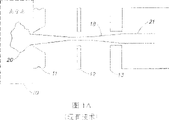
Figure 1A is the schematic diagram of the ion source extraction system of prior art;
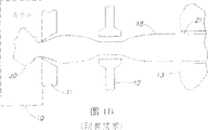
Figure 1B is the schematic diagram of the another kind of ion source extraction system of prior art;
Fig. 2 is the schematic diagram according to first embodiment of ion source extraction system of the present invention;
Fig. 3 is the schematic diagram according to second embodiment of ion source extraction system of the present invention;
Fig. 4 A shows according to the present invention to be used for the beam trajectory of embodiment of certain extraction system and the simulation curve of equipotential line;
Fig. 4 B is the phase curve of the ion beam showed in Fig. 4 A;
Fig. 4 C is the voltage curve that is used for the extraction system of Fig. 4 A displaying;
Fig. 4 D is the energy curve of the ion beam of Fig. 4 A displaying;
Fig. 5 A and 5B show the simulation curve of the equivalence of the extraction system that is used for Fig. 4 A of reconfiguring according to prior art;
Fig. 6 A shows according to the present invention to be used for the beam trajectory of embodiment of retarding lens and the simulation curve of equipotential line;
Fig. 6 B is the phase curve of the ion beam showed in Fig. 6 A; With
Fig. 7 is illustrated on the direction of crossing ion beam by the electrode of segmentation.
Detailed description of the present invention
Figure 1A and 1B are the schematic diagrames of prior art extraction system.The extraction system of Figure 1A is similar to low-energy industrial high current ion injected system, and the extraction system of Figure 1B is to show in above-mentioned people's such as Hiroyuki Ito paper.Similar element has identical reference number among Figure 1A and the 1B.Ion beam 18 is drawing from ion source 10.Each extraction system comprises first electrode 11, accelerating electrode 12 and retarding electrode 13.Plasma 20 also is demonstrated out.Plasma is by electronics and cation composition.Comprise that last ion beam adds that electronics and the cationic last beam-plasma 21 of heat also are demonstrated out.
Fig. 2 is the schematic diagram according to the low energy ion optical system of embodiment of the present invention.Figure 1A, 1B with 2 in similar element identical reference number is arranged.This system comprises first electrode 11, accelerating electrode 12, retarding electrode 113, electronics repel each other electrode 14 and last electrode 15.Plasma 20 is arranged in ion source 10.In the embodiment that ion-optic system is realized as the retarding lens system that is described below, plasma 20 is comprised the beam-plasma replacement of electronics, thermion and ion beam ion.The density of electronics and ion is such, so that ion beam 21 almost is a space charge neutrality.Ion beam ray 22 is illustrated in the general shape of ion-optic system intermediate ion bundle 18.
In this embodiment, the electronics in the beam-plasma 21 is presented electronics that near be enough to cause electronics repels each other electrode 14 on the bundle axis 19 current potential more is electronegative negative electricity than the current potential of the beam-plasma 21 at least electrode 14 that repels each other and stops and arrive retarding electrodes 13.In addition, the thermion in the beam-plasma 21 is presented the current potential that is enough to cause near the retarding electrode 13 bundle axis 19 more is electropositive positive electricity at least than the current potential of beam-plasma 21 retarding electrode 13 prevention arrival accelerating electrodes 12.Equally, retarding electrode 13 can be counted as stoping most of thermion to arrive accelerating electrode 12 by the bending that the edge at beam-plasma 21 causes.
Because the current potential that the thermion in the beam-plasma 21 is decelerated on the electrode 13 stops arrival accelerating electrode 12, so the hole of retarding electrode 13 can be greater than the hole of accelerating electrode 12.Therefore, formed virtual ion image is bigger than prior art ion extraction system, and the result is that the divergence of last low energy beams is reduced.Simultaneously, be greatly reduced for the electric current of accelerating electrode 12 from beam-plasma 21, so that the electric arc in the ion-optic system also is greatly reduced.
Fig. 3 is the ion-optic system schematic diagram according to another embodiment of the invention.Similar element has identical reference number in Figure 1A, 1B, 2 and 3.Except electronics repels each other magnetic element 24 that electrode 14 is used to stop electronics in the beam-plasma 21 to arrive retarding electrode 13 substitutes, Fig. 3 is similar to Fig. 2.Magnetic element 24 can comprise opposite pole shoe 24A and the 24b of magnetic polarity on the relative side that is positioned at ion beam 18, so that ion beam 18 passes magnetic field.Magnetic field stops the electronics in the beam-plasma 21 to arrive retarding electrode 13.
Except that than, the shape of retarding electrode 13 can be in order to reduce near the electric field of the bundle retarding electrode 13 on the axis 19 and selected.In one embodiment, the hole of retarding electrode 113 is towards accelerating electrode 12 angulations, and its axial width is selected like this, so that the electric field of restrainting on the axis 19 is reduced.Specifically, retarding electrode 13 can be to be shaped like this, with the size of pore as shown in Figure 3 towards downstream direction reduce gradually.
Fig. 2 and 3 ion-optic system are to describe in conjunction with draw ion beam 18 from ion source 10 in front.Yet the present invention is not limited to the ion source extraction system.Specifically, can be used as ion beam retarding lens system with that show in Fig. 2 and 3 and system class that described in front like ion-optic system and be used in any suitable position along beamline.Under the situation of retarding lens system, plasma 20 is the beam-plasmas in the retarding lens upstream.In the retarding lens system, similarly electrode configuration or electrode/magnetic element configurations can be utilized at the upstream termination of lens combination, and consequently 12 thermionic current is reduced from the beam-plasma to the accelerating electrode.Therefore, ion-optic system of the present invention can realize as ion source extraction system or retarding lens system.
Fig. 4 A shows that shown in Figure 2 being used for produces the two-dimensional analog of embodiment of the boron ion beam of the high electric current of 7keV.Such ion beam can be used to be expelled among the mass analysis magnet in ion implant systems.This simulation is to optimize at injecting the desired little divergence of mass spectral analysis magnet.Simulation comprises the thermal transpiration degree that is caused by the distinctive 1eV ion of such high current ion source.
Numeral on Fig. 4 A top is the negative value of the electrode voltage of ionogenic relatively plasma 20.In the simulation of Fig. 4 A, first electrode 11 is set at-59.5V.Accelerating electrode 12 is set at-30.0kV, and retarding electrode 13 is set at-3.4kV, and the electronics electrode 14 that repels each other is set at-8.4kV, and last electrode 15 is set at-7.0kV, and these voltages are the current potential appointment of relative ion source plasma 20 entirely.People will understand these voltages relatively current potential move up or down.In order to show in Fig. 4 C at the selected voltage of generation 7.0keV ion beam under the situation of earth potential (0kV) at last electrode 15.Example hereto, first electrode 11 adds+the 7.0kV bias voltage, and accelerating electrode 12 adds-the 23kV bias voltage, and retarding electrode 13 adds+the 3.6kV bias voltage, and the electronics electrode 14 that repels each other adds-the 1.4kV bias voltage, and last electrode 15 is grounded.Corresponding beam energy is showed in Fig. 4 D.In Fig. 4 D, dotted line is illustrated in the beam energy of the outside of beam as the function of distance (and electrode position), and solid line is illustrated in the beam energy of beam centre (on axis).As shown in the figure, ion beam is accelerated to about 25keV near accelerating electrode 12, is decelerated to about 6keV near retarding electrode 13, is accelerated to about 8keV near electronics repels each other electrode 14, and is decelerated to 7.0keV near last electrode 15.
In the simulation of Fig. 4 A, the voltage of retarding electrode 13 and undersize are to produce the voltage that is positive electricity with respect to beam-plasma 21 on axis 19.It is enough to make crescent 25 bending to reverse, so that most thermion of drawing from beam-plasma 21 will fly to the electronics electrode 14 that repels each other.Crescent 25 representatives become neutral point in fact along the beam line ion bundle.Therefore, most thermion is prevented from flying to accelerating electrode 12.The electronics electrode 14 that repels each other has the voltage (in this example, 1.4kV to 23kV) more much smaller than accelerating electrode 12 with respect to beam-plasma 21, and therefore malfunctioning (sparkover) is avoided.
The phase curve of the ion beam among Fig. 4 B exploded view 4A.Ion beam has the maximum divergence of 40 milliradians, and most beam has the divergence more much smaller than 40 milliradians.In the embodiment of Fig. 4 A, the voltage swing with respect to ground on retarding electrode 13 and electronics repel each other electrode 14 can be changed, so that realize greater or lesser divergence in ion beam.
Fig. 5 A and 5B show same ion-optic system, and wherein retarding electrode 13 and electronics repel each other electrode 14 under the current potential of ion beam, reconfigure the prior art systems of Figure 1A or 1B whereby effectively.Specifically, electrode 13,14 and 15 has equal bias voltage.This simulation shows than with the beam divergence that simulation obtained of Fig. 4 A and 4B the beam of Duoing, its maximum divergence is 100 milliradians, promptly as the 2.5 times big of simulation of Fig. 4 A and 4B.People are noted that in the configuration of the voltage ground connection on kind electrode 13 and 14, even reduce trip slit foot cun and reduce the source electric current and can not recover the low divergence seen in the simulation of Fig. 4 A and 4B.
Fig. 6 A and 6B show the two-dimensional analog according to the retarding lens system of embodiment of the present invention.In this embodiment, the ion-optic system of Fig. 6 A and 6B is positioned at ionogenic downstream.As in the simulation of Fig. 4 A, be the negative value of relative beam-plasma corresponding electrode voltage in the numeral of each electrode tip.In the embodiment of Fig. 6 A, first electrode 11 has-voltage of 3.0kV, accelerating electrode 12 has-voltage of 12.0kV, retarding electrode 13 has+voltage of 700V, the electronics electrode 14 that repels each other has-voltage of 1.2kV, and last electrode 15 has-and the voltage of 800V, all voltage all is the current potential appointment of relative beam source.
In the simulation softward on right side and the mistake in the routine be created in the mistake in crescent 25 but also make " wing " among Fig. 6 B become big.Yet people still can see the low divergence of generation.Divergence is near the thermoae limit that is caused in ion source by the 1eV ion.The current potential that retarding electrode 13 and electronics repel each other on the electrode 14 can change with respect to the earth potential of last beam, to realize the beam focus of expection.Electrode 13 and 14 use have also reduced for given focus requisite voltage on accelerating electrode 12.For lower beam current, perhaps for the beam that lower beam current is arranged partly,, can make the voltage on the retarding electrode 13 become negative (between the voltage of electrode 12 and 14) in order to reduce focusing.
Showed at Fig. 6 A with previously described retarding lens system in, accelerating electrode 12, retarding electrode 13 or both can be by segmentations in crossing the direction of ion beam.The embodiment of the accelerating electrode 12 of segmentation is showed in Fig. 7.Accelerating electrode 12 can be included in the electrode section 50,51,52,53 and 54 and be positioned at electrode section 60,61,62,63 and 64 below the ion beam 18 of ion beam 18 tops.The number of electrode section and size can be selected at specific application.In addition, partly or entirely may can be added on each electrode section by identical or different independently voltage, to achieve desired results.Use the electrode of segmentation, last beam density and the focus of each part of beam can be adjusted.For example, more be electronegative voltage if the fragment of certain given electrode 12 has than two adjacent electrode sections, the beam current density by this fragment is increased and focuses on also and is increased so.Similarly, more be electropositive voltage if the fragment of given electrode 13 has than two adjacent electrode sections, the beam current density by this fragment is reduced to focus on and is increased so.Therefore, by regulating the voltage on each fragment, the density of beam and focus both can be adjusted.If the voltage on each fragment of adjusting electrode 12 and 13, focus can be adjusted so.If each voltage is all born with respect to last ground on electrode 13, the electronics electrode 14 that repels each other can be cancelled so.Can be in line also can hand over across the position of each electrode section of ion beam 22 and borrow.
Although showed and described the preferred embodiments of the invention of considering at present, it is evident that for the people who is familiar with this technology not breaking away from the defined scope of the present invention of claims can finish various variation and correction.
Claims (11)
1. ion optics that is used for producing the low energy ion beam of bundle axis, this ion beam has beam-plasma, and described device comprises:
Be used for making the accelerating electrode of ion beam acceleration;
Be used for making the retarding electrode of ion beam deceleration in described accelerating electrode downstream, described retarding electrode has in order to stop thermion to arrive described accelerating electrode provides barrier potential and selected voltage for the thermion in the beam-plasma; And
Be used for stoping electronics in the beam-plasma to arrive the ion optical element of described retarding electrode in described retarding electrode downstream, described ion optical element comprises the electronics electrode that repels each other, this electronics repel each other that electrode has selected like this voltage so that near electronics repels each other electrode the current potential on the bundle axis more be negative electricity than the current potential of beam-plasma at least.
2. according to the ion optics of claim 1, wherein ion beam has the bundle axis, and retarding electrode voltage is selected like this, so that the current potential near the bundle axis the described retarding electrode more is positive electricity than the current potential of beam-plasma at least.
3. according to the ion optics of claim 1, wherein said retarding electrode is shaped for restriction electric field on the bundle axis.
4. according to the ion optics of claim 1, the hole of wherein said retarding electrode is greater than the hole of described accelerating electrode.
5. according to the ion optics of claim 1, have at least one crossing on the direction of ion beam in the middle of wherein said accelerating electrode and the described retarding electrode by segmentation, so that define separately controllable electrode section.
6. according to the ion optics of claim 1, it is realized as the ion source extraction system.
7. according to the ion optics of claim 1, it is realized as the retarding lens system.
8. method that is used for producing the low energy ion beam of bundle axis, wherein ion beam has beam-plasma, and described method comprises the steps:
With accelerating electrode ion beam is quickened;
The retarding electrode that is used in the accelerating electrode downstream is slowed down ion beam;
Add in order to stop thermion arrival accelerating electrode to provide barrier potential and selected bias voltage for the thermion in the beam-plasma to retarding electrode; And
Stop the electronics in the beam-plasma to arrive retarding electrode with the repel each other ion optical element of electrode of the electronics that is included in the retarding electrode downstream, stop the step of electronics further to comprise the repel each other voltage of electrode of so selected electronics, so that the current potential on the bundle axis more is negative electricity than the current potential of beam-plasma at least near electronics repels each other electrode.
9. method according to Claim 8, wherein ion beam has the bundle axis, and comprises that such selection retarding electrode voltage so that the current potential near the bundle axis retarding electrode more are positive electricity than the current potential of beam-plasma at least for the biased step of retarding electrode.
10. method according to Claim 8 further comprises the step that retarding electrode is shaped for the electric field that limits on the bundle axis.
11. method according to Claim 8 further comprises will speed up one of electrode and retarding electrode at least in the step of crossing segmentation on the direction of ion beam.
Applications Claiming Priority (3)
| Application Number | Priority Date | Filing Date | Title |
|---|---|---|---|
| US71693100A | 2000-11-20 | 2000-11-20 | |
| US09/716,931 | 2000-11-20 | ||
| PCT/US2001/043205 WO2002043103A2 (en) | 2000-11-20 | 2001-11-20 | Extraction and deceleration of low energy beam with low beam divergence |
Publications (2)
| Publication Number | Publication Date |
|---|---|
| CN1565043A CN1565043A (en) | 2005-01-12 |
| CN1311508C true CN1311508C (en) | 2007-04-18 |
Family
ID=24880034
Family Applications (1)
| Application Number | Title | Priority Date | Filing Date |
|---|---|---|---|
| CNB018213774A Expired - Lifetime CN1311508C (en) | 2000-11-20 | 2001-11-20 | Extraction and deceleration of low energy beam with low beam divergence |
Country Status (8)
| Country | Link |
|---|---|
| US (1) | US6838677B2 (en) |
| EP (1) | EP1336188B1 (en) |
| JP (1) | JP3844301B2 (en) |
| KR (1) | KR100843805B1 (en) |
| CN (1) | CN1311508C (en) |
| DE (1) | DE60104716T2 (en) |
| TW (1) | TW543071B (en) |
| WO (1) | WO2002043103A2 (en) |
Families Citing this family (20)
| Publication number | Priority date | Publication date | Assignee | Title |
|---|---|---|---|---|
| JP3827132B2 (en) * | 1999-07-30 | 2006-09-27 | 株式会社 Sen−Shi・アクセリス カンパニー | Ion implantation apparatus and ion implantation method |
| US7087913B2 (en) * | 2003-10-17 | 2006-08-08 | Applied Materials, Inc. | Ion implanter electrodes |
| US7598505B2 (en) * | 2005-03-08 | 2009-10-06 | Axcelis Technologies, Inc. | Multichannel ion gun |
| US7361913B2 (en) * | 2005-04-02 | 2008-04-22 | Varian Semiconductor Equipment Associates, Inc. | Methods and apparatus for glitch recovery in stationary-beam ion implantation process using fast ion beam control |
| US7339179B2 (en) * | 2005-11-15 | 2008-03-04 | Varian Semiconductor Equipment Associates, Inc. | Technique for providing a segmented electrostatic lens in an ion implanter |
| US7675047B2 (en) * | 2005-11-15 | 2010-03-09 | Varian Semiconductor Equipment Associates, Inc. | Technique for shaping a ribbon-shaped ion beam |
| GB0612915D0 (en) * | 2006-06-30 | 2006-08-09 | Nordiko Technical Services Ltd | Apparatus |
| JP5337028B2 (en) * | 2006-06-30 | 2013-11-06 | ノルディコ テクニカル サーヴィシズ リミテッド | apparatus |
| GB0703044D0 (en) * | 2007-02-16 | 2007-03-28 | Nordiko Technical Services Ltd | Apparatus |
| KR100978793B1 (en) | 2008-11-19 | 2010-08-30 | 한국원자력연구원 | Low energy, high current and large beam extraction and transport device using multiple accel-decel electrodes |
| US7888653B2 (en) * | 2009-01-02 | 2011-02-15 | Varian Semiconductor Equipment Associates, Inc. | Techniques for independently controlling deflection, deceleration and focus of an ion beam |
| CN101899645B (en) * | 2009-06-01 | 2014-05-21 | 无锡华润上华半导体有限公司 | Ion implantation method |
| CN101861048B (en) * | 2010-03-05 | 2012-09-05 | 哈尔滨工业大学 | Method for focusing plasma beam under magnetic lens |
| JP5500500B2 (en) * | 2010-03-11 | 2014-05-21 | 日新イオン機器株式会社 | Ion implanter with beam deflector having asymmetric Einzel lens |
| US20140127394A1 (en) * | 2012-11-07 | 2014-05-08 | Varian Semiconductor Equipment Associates, Inc. | Reducing Glitching In An Ion Implanter |
| CN103779164B (en) * | 2013-11-08 | 2015-12-02 | 北京中科信电子装备有限公司 | A kind of beam deceleration device |
| JP6257411B2 (en) * | 2014-03-27 | 2018-01-10 | 住友重機械イオンテクノロジー株式会社 | Ion implantation apparatus, final energy filter, and ion implantation method |
| US10074514B1 (en) * | 2017-09-08 | 2018-09-11 | Varian Semiconductor Equipment Associates, Inc. | Apparatus and method for improved ion beam current |
| US11251075B2 (en) * | 2018-08-06 | 2022-02-15 | Mattson Technology, Inc. | Systems and methods for workpiece processing using neutral atom beams |
| CN113278930B (en) * | 2021-04-25 | 2023-04-18 | 北京航空航天大学合肥创新研究院(北京航空航天大学合肥研究生院) | Nanocluster beam density control device and application method thereof |
Citations (5)
| Publication number | Priority date | Publication date | Assignee | Title |
|---|---|---|---|---|
| JPH01209645A (en) * | 1988-02-16 | 1989-08-23 | Toshiba Corp | Ion source and electron gun |
| CN1132407A (en) * | 1994-11-04 | 1996-10-02 | 株式会社日立制作所 | Surface treatment method and system |
| US5748360A (en) * | 1995-03-06 | 1998-05-05 | National Research Institute For Metals | Decelerating and focusing ion beam device |
| US5869838A (en) * | 1996-09-11 | 1999-02-09 | Advanced Lithography Group | Field composable electrostatic lens system |
| US5969366A (en) * | 1995-11-08 | 1999-10-19 | Applied Materials, Inc. | Ion implanter with post mass selection deceleration |
Family Cites Families (13)
| Publication number | Priority date | Publication date | Assignee | Title |
|---|---|---|---|---|
| US4146810A (en) | 1977-12-29 | 1979-03-27 | International Business Machines Corporation | Radiation heated acceleration |
| JPH01132033A (en) * | 1987-11-17 | 1989-05-24 | Hitachi Ltd | Ion source |
| US4933551A (en) * | 1989-06-05 | 1990-06-12 | The United State Of America As Represented By The Administrator Of The National Aeronautics And Space Administration | Reversal electron attachment ionizer for detection of trace species |
| US5196706A (en) | 1991-07-30 | 1993-03-23 | International Business Machines Corporation | Extractor and deceleration lens for ion beam deposition apparatus |
| JPH05144397A (en) | 1991-11-20 | 1993-06-11 | Mitsubishi Electric Corp | Ion source |
| US5365070A (en) * | 1992-04-29 | 1994-11-15 | The Regents Of The University Of California | Negative ion beam injection apparatus with magnetic shield and electron removal means |
| US5780862A (en) | 1994-01-11 | 1998-07-14 | Siess; Harold E. | Method and apparatus for generating ions |
| GB2343547B (en) | 1995-11-08 | 2000-06-21 | Applied Materials Inc | An ion implanter with substrate neutralizer |
| GB2307592B (en) | 1995-11-23 | 1999-11-10 | Applied Materials Inc | Ion implantation apparatus withimproved post mass selection deceleration |
| US5729028A (en) | 1997-01-27 | 1998-03-17 | Rose; Peter H. | Ion accelerator for use in ion implanter |
| KR100249307B1 (en) | 1997-05-13 | 2000-03-15 | 윤종용 | Analyzer of Ion implanting apparatus |
| DE19929278A1 (en) * | 1998-06-26 | 2000-02-17 | Nissin Electric Co Ltd | Negative hydrogen ion beam injection method on substrate |
| JP2002525820A (en) | 1998-09-24 | 2002-08-13 | コーニンクレッカ フィリップス エレクトロニクス エヌ ヴィ | Ion implanter arranged to select neutral ions from ion beam |
-
2001
- 2001-11-20 JP JP2002544749A patent/JP3844301B2/en not_active Expired - Fee Related
- 2001-11-20 US US09/988,565 patent/US6838677B2/en not_active Expired - Lifetime
- 2001-11-20 KR KR1020037006776A patent/KR100843805B1/en active IP Right Grant
- 2001-11-20 CN CNB018213774A patent/CN1311508C/en not_active Expired - Lifetime
- 2001-11-20 EP EP01997829A patent/EP1336188B1/en not_active Expired - Lifetime
- 2001-11-20 TW TW090128683A patent/TW543071B/en not_active IP Right Cessation
- 2001-11-20 DE DE60104716T patent/DE60104716T2/en not_active Expired - Fee Related
- 2001-11-20 WO PCT/US2001/043205 patent/WO2002043103A2/en active IP Right Grant
Patent Citations (5)
| Publication number | Priority date | Publication date | Assignee | Title |
|---|---|---|---|---|
| JPH01209645A (en) * | 1988-02-16 | 1989-08-23 | Toshiba Corp | Ion source and electron gun |
| CN1132407A (en) * | 1994-11-04 | 1996-10-02 | 株式会社日立制作所 | Surface treatment method and system |
| US5748360A (en) * | 1995-03-06 | 1998-05-05 | National Research Institute For Metals | Decelerating and focusing ion beam device |
| US5969366A (en) * | 1995-11-08 | 1999-10-19 | Applied Materials, Inc. | Ion implanter with post mass selection deceleration |
| US5869838A (en) * | 1996-09-11 | 1999-02-09 | Advanced Lithography Group | Field composable electrostatic lens system |
Also Published As
| Publication number | Publication date |
|---|---|
| KR20030084901A (en) | 2003-11-01 |
| WO2002043103A2 (en) | 2002-05-30 |
| WO2002043103A8 (en) | 2004-02-26 |
| WO2002043103A3 (en) | 2002-10-17 |
| KR100843805B1 (en) | 2008-07-03 |
| TW543071B (en) | 2003-07-21 |
| JP2004525480A (en) | 2004-08-19 |
| JP3844301B2 (en) | 2006-11-08 |
| DE60104716D1 (en) | 2004-09-09 |
| DE60104716T2 (en) | 2005-01-27 |
| EP1336188B1 (en) | 2004-08-04 |
| CN1565043A (en) | 2005-01-12 |
| EP1336188A2 (en) | 2003-08-20 |
| US6838677B2 (en) | 2005-01-04 |
| US20020089288A1 (en) | 2002-07-11 |
Similar Documents
| Publication | Publication Date | Title |
|---|---|---|
| CN1311508C (en) | Extraction and deceleration of low energy beam with low beam divergence | |
| TWI686840B (en) | Combined electrostatic lens system for ion implantation | |
| US8124946B2 (en) | Post-decel magnetic energy filter for ion implantation systems | |
| CN1149623C (en) | Accelerator-decelerator electrostatic lens for variably focusing and mass resolving ion beam in ion implanter | |
| JP5120598B2 (en) | Acceleration / deceleration gap for deflection | |
| JP3727047B2 (en) | Ion implanter | |
| US7339179B2 (en) | Technique for providing a segmented electrostatic lens in an ion implanter | |
| JP2002517885A (en) | Acceleration and analysis architecture for ion implanters | |
| EP1046183B1 (en) | Ion implantation device arranged to select neutral ions from the ion beam and methode | |
| TW201214500A (en) | Deceleration lens | |
| KR20210078565A (en) | How to control an ion implanter, an ion beam, and an ion implanter | |
| KR20120049883A (en) | Adjustable louvered plasma electron flood enclosure | |
| JP2007507077A (en) | Extraction method of ion beam slit with mass separation | |
| US20060169911A1 (en) | Electron confinement inside magent of ion implanter | |
| JP6656260B2 (en) | Apparatus and method for controlling ion beam current for processing a substrate and ion implanter | |
| JP7268003B2 (en) | Apparatus, system and method for ion implantation | |
| WO2022086670A1 (en) | System and technique for creating implanted regions using multiple tilt angles | |
| JPH0693352B2 (en) | Ion implanter | |
| US10804068B2 (en) | Electostatic filter and method for controlling ion beam properties using electrostatic filter | |
| JPH04284343A (en) | Device and method of ion beam irradiation | |
| JPH087813A (en) | Ion implanting device |
Legal Events
| Date | Code | Title | Description |
|---|---|---|---|
| C06 | Publication | ||
| PB01 | Publication | ||
| C10 | Entry into substantive examination | ||
| SE01 | Entry into force of request for substantive examination | ||
| C14 | Grant of patent or utility model | ||
| GR01 | Patent grant | ||
| CX01 | Expiry of patent term | ||
| CX01 | Expiry of patent term |
Granted publication date: 20070418 |