CN1311283C - Liquid crystal display - Google Patents
Liquid crystal display Download PDFInfo
- Publication number
- CN1311283C CN1311283C CNB028214773A CN02821477A CN1311283C CN 1311283 C CN1311283 C CN 1311283C CN B028214773 A CNB028214773 A CN B028214773A CN 02821477 A CN02821477 A CN 02821477A CN 1311283 C CN1311283 C CN 1311283C
- Authority
- CN
- China
- Prior art keywords
- liquid crystal
- crystal cells
- optical compensatory
- compensatory element
- polaroid
- Prior art date
- Legal status (The legal status is an assumption and is not a legal conclusion. Google has not performed a legal analysis and makes no representation as to the accuracy of the status listed.)
- Expired - Fee Related
Links
Images


Classifications
-
- G—PHYSICS
- G02—OPTICS
- G02F—OPTICAL DEVICES OR ARRANGEMENTS FOR THE CONTROL OF LIGHT BY MODIFICATION OF THE OPTICAL PROPERTIES OF THE MEDIA OF THE ELEMENTS INVOLVED THEREIN; NON-LINEAR OPTICS; FREQUENCY-CHANGING OF LIGHT; OPTICAL LOGIC ELEMENTS; OPTICAL ANALOGUE/DIGITAL CONVERTERS
- G02F1/00—Devices or arrangements for the control of the intensity, colour, phase, polarisation or direction of light arriving from an independent light source, e.g. switching, gating or modulating; Non-linear optics
- G02F1/01—Devices or arrangements for the control of the intensity, colour, phase, polarisation or direction of light arriving from an independent light source, e.g. switching, gating or modulating; Non-linear optics for the control of the intensity, phase, polarisation or colour
- G02F1/13—Devices or arrangements for the control of the intensity, colour, phase, polarisation or direction of light arriving from an independent light source, e.g. switching, gating or modulating; Non-linear optics for the control of the intensity, phase, polarisation or colour based on liquid crystals, e.g. single liquid crystal display cells
- G02F1/133—Constructional arrangements; Operation of liquid crystal cells; Circuit arrangements
- G02F1/1333—Constructional arrangements; Manufacturing methods
- G02F1/1335—Structural association of cells with optical devices, e.g. polarisers or reflectors
- G02F1/13363—Birefringent elements, e.g. for optical compensation
-
- G—PHYSICS
- G02—OPTICS
- G02F—OPTICAL DEVICES OR ARRANGEMENTS FOR THE CONTROL OF LIGHT BY MODIFICATION OF THE OPTICAL PROPERTIES OF THE MEDIA OF THE ELEMENTS INVOLVED THEREIN; NON-LINEAR OPTICS; FREQUENCY-CHANGING OF LIGHT; OPTICAL LOGIC ELEMENTS; OPTICAL ANALOGUE/DIGITAL CONVERTERS
- G02F1/00—Devices or arrangements for the control of the intensity, colour, phase, polarisation or direction of light arriving from an independent light source, e.g. switching, gating or modulating; Non-linear optics
- G02F1/01—Devices or arrangements for the control of the intensity, colour, phase, polarisation or direction of light arriving from an independent light source, e.g. switching, gating or modulating; Non-linear optics for the control of the intensity, phase, polarisation or colour
- G02F1/13—Devices or arrangements for the control of the intensity, colour, phase, polarisation or direction of light arriving from an independent light source, e.g. switching, gating or modulating; Non-linear optics for the control of the intensity, phase, polarisation or colour based on liquid crystals, e.g. single liquid crystal display cells
- G02F1/137—Devices or arrangements for the control of the intensity, colour, phase, polarisation or direction of light arriving from an independent light source, e.g. switching, gating or modulating; Non-linear optics for the control of the intensity, phase, polarisation or colour based on liquid crystals, e.g. single liquid crystal display cells characterised by the electro-optical or magneto-optical effect, e.g. field-induced phase transition, orientation effect, guest-host interaction or dynamic scattering
- G02F1/139—Devices or arrangements for the control of the intensity, colour, phase, polarisation or direction of light arriving from an independent light source, e.g. switching, gating or modulating; Non-linear optics for the control of the intensity, phase, polarisation or colour based on liquid crystals, e.g. single liquid crystal display cells characterised by the electro-optical or magneto-optical effect, e.g. field-induced phase transition, orientation effect, guest-host interaction or dynamic scattering based on orientation effects in which the liquid crystal remains transparent
- G02F1/1396—Devices or arrangements for the control of the intensity, colour, phase, polarisation or direction of light arriving from an independent light source, e.g. switching, gating or modulating; Non-linear optics for the control of the intensity, phase, polarisation or colour based on liquid crystals, e.g. single liquid crystal display cells characterised by the electro-optical or magneto-optical effect, e.g. field-induced phase transition, orientation effect, guest-host interaction or dynamic scattering based on orientation effects in which the liquid crystal remains transparent the liquid crystal being selectively controlled between a twisted state and a non-twisted state, e.g. TN-LC cell
- G02F1/1397—Devices or arrangements for the control of the intensity, colour, phase, polarisation or direction of light arriving from an independent light source, e.g. switching, gating or modulating; Non-linear optics for the control of the intensity, phase, polarisation or colour based on liquid crystals, e.g. single liquid crystal display cells characterised by the electro-optical or magneto-optical effect, e.g. field-induced phase transition, orientation effect, guest-host interaction or dynamic scattering based on orientation effects in which the liquid crystal remains transparent the liquid crystal being selectively controlled between a twisted state and a non-twisted state, e.g. TN-LC cell the twist being substantially higher than 90°, e.g. STN-, SBE-, OMI-LC cells
-
- G—PHYSICS
- G02—OPTICS
- G02F—OPTICAL DEVICES OR ARRANGEMENTS FOR THE CONTROL OF LIGHT BY MODIFICATION OF THE OPTICAL PROPERTIES OF THE MEDIA OF THE ELEMENTS INVOLVED THEREIN; NON-LINEAR OPTICS; FREQUENCY-CHANGING OF LIGHT; OPTICAL LOGIC ELEMENTS; OPTICAL ANALOGUE/DIGITAL CONVERTERS
- G02F1/00—Devices or arrangements for the control of the intensity, colour, phase, polarisation or direction of light arriving from an independent light source, e.g. switching, gating or modulating; Non-linear optics
- G02F1/01—Devices or arrangements for the control of the intensity, colour, phase, polarisation or direction of light arriving from an independent light source, e.g. switching, gating or modulating; Non-linear optics for the control of the intensity, phase, polarisation or colour
- G02F1/13—Devices or arrangements for the control of the intensity, colour, phase, polarisation or direction of light arriving from an independent light source, e.g. switching, gating or modulating; Non-linear optics for the control of the intensity, phase, polarisation or colour based on liquid crystals, e.g. single liquid crystal display cells
- G02F1/133—Constructional arrangements; Operation of liquid crystal cells; Circuit arrangements
- G02F1/1333—Constructional arrangements; Manufacturing methods
- G02F1/1335—Structural association of cells with optical devices, e.g. polarisers or reflectors
- G02F1/13363—Birefringent elements, e.g. for optical compensation
- G02F1/133636—Birefringent elements, e.g. for optical compensation with twisted orientation, e.g. comprising helically oriented LC-molecules or a plurality of twisted birefringent sublayers
-
- G—PHYSICS
- G02—OPTICS
- G02F—OPTICAL DEVICES OR ARRANGEMENTS FOR THE CONTROL OF LIGHT BY MODIFICATION OF THE OPTICAL PROPERTIES OF THE MEDIA OF THE ELEMENTS INVOLVED THEREIN; NON-LINEAR OPTICS; FREQUENCY-CHANGING OF LIGHT; OPTICAL LOGIC ELEMENTS; OPTICAL ANALOGUE/DIGITAL CONVERTERS
- G02F2202/00—Materials and properties
- G02F2202/40—Materials having a particular birefringence, retardation
Landscapes
- Physics & Mathematics (AREA)
- Nonlinear Science (AREA)
- Chemical & Material Sciences (AREA)
- Crystallography & Structural Chemistry (AREA)
- General Physics & Mathematics (AREA)
- Optics & Photonics (AREA)
- Mathematical Physics (AREA)
- Spectroscopy & Molecular Physics (AREA)
- Liquid Crystal (AREA)
- Polarising Elements (AREA)
Abstract
A liquid crystal display device comprises a liquid crystal cell, polarizers disposed on both sides of the liquid crystal cell, and an optical compensation element disposed on at least one side of the liquid crystal cell between the liquid crystal cell and the polarizers, wherein the twist angle of the liquid crystal layer in the liquid crystal cell is set to from 180 to 270 degrees; the optical compensating element has a twisted structure twisted in the opposite direction to that of the liquid crystal layer; the difference in the absolute values of the twist angles between the liquid crystal cell and the optical compensation element is from 40 to 100 degrees; the difference in retardation at a wavelength lambda=550 nm between the liquid crystal cell and the optical compensation element is from 100 to 250 nm; and the ratio of the absolute values of the differences in retardation at wavelengths lambda of 400 nm and 550 nm between the liquid crystal cell and the optical compensation element is within the range of 0.5 to 1.0. The liquid crystal display devices provide a white display with high contrast and excellent brightness and hue in the normally black mode and provide a paper-white white display and an excellent black display in the normally black mode.
Description
Technical field
The application relates to the liquid crystal indicator that can show with transmission, reflection or Transflective pattern.
Background technology
Widely used liquid crystal display (below be called " LCD ") device is TFT (thin film transistor (TFT)) or TFD (thin film diode) type, it shows with plurality of display modes such as TN (twisted-nematic), VA (vertical orientated) and IPS (switching face in) pattern under the active matrix mode of using TFT or TFD element, and the STN type that shows with STN (supertwist is to being listed as) liquid crystal display pattern under the passive matrix mode.
TFT and TFD type LCD device are characterised in that to have fabulous picture quality and response speed, are widely used in laptop computer, LCD monitor or the LCD TV receiver.But, although it is poor slightly that STN type LCD device is compared with the TFT type aspect picture quality and response speed, but, can make at lower cost, and be widely used as the display of mobile phone, personal digital assistant, mobile personal computer and mobile TV receiver because it is simple in structure and power consumption is less.
The general such formation of above-mentioned STN type liquid crystal indicator, promptly liquid crystal cells is clipped between a pair of polaroid, and when being used for reflection-type liquid-crystal display device, further at outer setting one reflector plate of each polaroid.
STN type liquid crystal display (following can be called " STN-LCD ") device, because its displaying principle has been utilized optical activity and birefringence, therefore shown color inevitably can undesirable coloration.In order to carry out white and black displays under the situation of above-mentioned coloring problem and further to carry out colored the demonstration overcoming, be extensive use of the method that compensates with optical element.At first, use a kind of so-called double-deck liquid crystal mode (D-STN:Double-layer STN), wherein be provided with the delay liquid crystal cells that is used to compensate, this delay liquid crystal cells has the delay (product of birefringence n and bed thickness d) that equals to drive liquid crystal cells substantially, and have twist angle and driver element equal and opposite in direction and the opposite distorted-structure of torsional direction, make and drive and the oriented adjacent axle of compensation liquid crystal cells (the Osamu Okumura that meets at right angles, Television Gakkai TechnicalReport, 11,79 (1987); K.Katou, Jpn.J.Appl.Phys., 26, L17,784 (1987); Y.Nagase, SID Digest, 1989).
Although this method can obtain the high-contrast display, but it only has been used very short time, because owing to use two liquid crystal cells, it has the shortcoming that increases LCD installation cost, weight and thickness.At present, the method for using a kind of optical delay film that obtains by accurate stretching polymer film such as polycarbonate to carry out pseudo-compensation.Although use the method for this optical delay film simple and cheap, but owing to do not have the distortion molecular orientation in the optical delay film, it has the problem of fully avoiding the undesirable painted demonstration of STN-LCD device.
At the open No.3-87720 of Japanese unexamined patent publication No., 3-291620,3-291623 has disclosed among 3-294821 and the 4-003020 and has used liquid crystal film with the fixing twisted nematic liquid crystal orientation method as optical compensation films, as the third compensation method.Have distorted-structure between the molecule of this optical compensation films, from but a kind of excellent compensation effect that method obtained that has the using compensation liquid crystal cells concurrently and uses the advantage of optical compensation film method, promptly be easy to use and fabulous cheaply film.
The principle of this compensation method and D-STN method are similar, and compensate during non-selection voltage applies.Thereby, because during non-selection voltage applies, the polarization state of light of passing light incident side polaroid, optical compensation films and driving liquid crystal cells in all wavelengths all by linear polarization, thereby in normal black (being black during the non-selection voltage) and normal white (being white during the non-selection voltage) pattern, by suitably selecting the absorption axes position of outgoing side polaroid respectively, can obtaining basically, the black display and the best basically white of the best show.
On the other hand, with different during non-selection voltage applies, during selecting voltage to apply, pass the polarization state of light of light incident side polaroid, optical compensation films and driving liquid crystal cells by elliptic polarization.In addition, the ovality of elliptically polarized light and position angle become with wavelength.Therefore, with different during non-selection voltage applies, owing in normal black pattern or normal white mode, can not provide best white or black display, the optical devices that need research to be more suitable for during selecting voltage to apply.
The object of the present invention is to provide a kind of liquid crystal indicator, it can be provided in the normal black pattern has fabulous brightness and tone, has in normal white mode that bright blank sheet of paper shape shows and the white display of high-contrast of fabulous black display.
Summary of the invention
According to first aspect present invention, a kind of liquid crystal indicator that comprises liquid crystal cells is provided, wherein liquid crystal cells is made of a pair of liquid crystal material layer that all has the transparency carrier of electrode and be clipped between the substrate, polaroid is arranged on the liquid crystal cells both sides, at least one surface that optical compensatory element is arranged on liquid crystal cells is gone up and is between liquid crystal cells and the polaroid, from two or more voltages, select voltage, driving voltage is applied on the liquid crystal material layer, and wherein the torsion angle of liquid crystal cells is made as 180 to 270 degree; Optical compensatory element has along the torsion structure that reverses with the liquid crystal cells reverse direction; The absolute value of the windup-degree between liquid crystal cells and the optical compensatory element poor is 40 to 100 degree; The difference of the delay when wavelength X=550nm between liquid crystal cells and the optical compensatory element is 100 to 250nm; And the absolute value of the difference of the delay of liquid crystal cells and optical compensatory element was expressed as Δ R (400) and Δ R (550) respectively when wavelength X was 400nm and 550nm, represent the ratio D between them with D=Δ R (400)/Δ R (550), D is in 0.5 to 1.0 scope.
According to second aspect present invention, a kind of liquid crystal indicator according to first aspect is provided, wherein this optical compensatory element is a liquid crystal film.
Below the present invention will be described in more detail.
Liquid crystal indicator of the present invention comprises liquid crystal cells; Be arranged on the polaroid of its both sides; And be arranged on optical compensatory element between at least one side of liquid crystal cells, liquid crystal cells and the polaroid.
This liquid crystal cells has the liquid crystal material layer that is clipped between a pair of transparency carrier that has electrode respectively.Operable transparency carrier among the present invention is for making the substrate of liquid crystal material orientation.The substrate of example for liquid crystal material is orientated, and substrate more specifically with the oriented layer that can make the liquid crystal material orientation.A pair of this transparency carrier with alignment capability is arranged to its direction of orientation reverses, between substrate, form one deck liquid crystal material (liquid crystal material layer), thereby form the liquid crystal material layer of specific windup-degree.Electrode is arranged on transparency carrier and the surface that the liquid crystal material layer contacts usually.Have in the situation of transparency carrier of oriented layer in use, electrode is arranged between oriented layer and the transparency carrier.Spendable liquid crystal material is for being used for the multiple material of STN-LCD among the present invention.
In liquid crystal indicator of the present invention, from two or more voltages, select voltage and apply driving voltage at the liquid crystal material layer.Be not particularly limited for described two or more voltages, as long as they are virtual voltages of actual execution liquid crystal display.Thereby described two or more magnitudes of voltage can be before reflectivity and transmissivity take place to change fast and magnitude of voltage afterwards.As a result, the liquid crystal material layer is as the active optical layer that demonstration is provided under white state (bright attitude) and black state (dark attitude).
Hope and is in 1100nm or the lower scope in the delay of 550nm af at wavelength lambda liquid crystal cells is in 600nm or higher scope.Postpone to be lower than the liquid crystal cells of 600nm, the state of liquid crystal changes smaller when applying voltage.The response of liquid crystal cells that postpones to be higher than 1100nm is relatively poor.
The polaroid that constitutes liquid crystal indicator of the present invention is arranged on the liquid crystal cells both sides.Polaroid is had no particular limits, thereby can be the normal polaroid that uses in the LCD.Object lesson is PVA (polyvinyl alcohol (PVA)) base-polarizing coating, as PVA and part acetal PVA; The polarizing coating that the hydrophilic polymer membrane of the partly-hydrolysed product by will comprising the ethylene vinyl acetate copolymer (ehtylene-vinylacetate copolymer) that is absorbed with iodine and/or dichroic dyestuff stretches and obtains; And the polarizing coating that comprises the polyenoid alignment films, as the dehydration product of PVA and the dehydrochlorination product of Polyvinylchloride.
Polaroid can use separately, perhaps can be arranged on one or two surface with being used to strengthen intensity, corrosion stability and stable on heating protective seam.Can be directly or via tacky adhesion or the stacked overlay of adhesive linkage such as polyester and tri acetyl cellulose; Resin coating layer; With acrylic acid or epoxy radicals light-cured type resin bed and form protective clear layer.When protective seam was coated on two surfaces of polarizing coating, they can be identical or different.
In the present invention, optical compensatory element is arranged at least one side and is between liquid crystal cells and the polaroid.Optical compensatory element has distorted-structure.That is, optical compensatory element has the structure that a kind of direction of orientation from a surface to another surface molecular twists, and is similar with the liquid crystal cells of TN pattern or STN pattern.Though can use the liquid crystal cells that is used to compensate or liquid crystal film as optical compensatory element, but this element can be one to have the film of pseudo-torsion structure, its optical delay film by stacked a large amount of uniaxial tensions obtains, and wherein the angle of the tensile axis of each phase shift films changes gradually.
In liquid crystal indicator of the present invention, use optical compensatory element with torsion structure and optical parametric optimization.Using traditional D-STN method under normal black pattern, to drive in the situation of transmission-type STN-LCD device, optical compensatory element with torsion structure as used herein has following parameter: its windup-degree is identical with the absolute value of the windup-degree of liquid crystal cells, but the torsion angle that torsional direction is opposite with liquid crystal cells, and delay equals or is slightly smaller than the delay of liquid crystal cells.
And employed optical compensatory element has a kind of like this torsion structure among the present invention, and its torsional direction is opposite with the torsional direction of liquid crystal cells; The difference of the absolute value of windup-degree is 40 to 100 degree between liquid crystal cells and the optical compensatory element, is preferably 45 to 75 degree; Difference in the delay of 550nm af at wavelength lambda liquid crystal cells and optical compensatory element is 100 to 250nm, is preferably 120 to 200nm.If the difference of the delay between 550nm af at wavelength lambda liquid crystal cells and the optical compensatory element departs from these scopes, then the display device that is produced shows to a certain extent, but compares with conventional apparatus, and contrast greatly reduces.
To the reason that adopt above-mentioned parameter be described briefly.
Torsional direction at optical compensatory element is opposite with liquid crystal cells, and in the situation that its pitch equates substantially, be provided with and be overlapped into liquid crystal cells and the optical compensatory element that its oriented adjacent axle is met at right angle substantially, can regard one as and reverse optically anisotropic body.The torsion angle of optically anisotropic body and postpone can approach the poor of the torsion angle of liquid crystal cells and optical compensatory element and delay.Its thinking is arranged to make its oriented adjacent axle to meet at right angle with two single shaft optical delay films that will have different delays, whole stacked phase shift films can be regarded an optically anisotropic body as, and its delay can to regard the difference that two uniaxial retardation film postpone as identical.Thereby, use this single stacked optically anisotropic body to seek the The optimal compensation condition.
Now, being arranged on a slice at polaroid reverses in the situation on the optically anisotropic body both sides, as shown in formula (1), can draw transmissivity " T " (E.P.Raynes, Mol.Cryst.Liq.Cryst.Lett., Vol.4 by 2 * 2 matrix methods that are called the Jones vector, 69 (1987), A.Lien, IEEE Trans.Electron Devices, Vol.36, No.9,1910 (1989)):
The relation of the axle of expression polaroid and optically anisotropic body among Fig. 1.Promptly, Reference numeral 11 expression optically anisotropic bodies are near the axis of orientation of light incident side polaroid one side, Reference numeral 12 expression optically anisotropic bodies are near the axis of orientation of outgoing side polaroid one side, the absorption axes of Reference numeral 13 expression light incident side polaroids, the absorption axes of Reference numeral 14 expression outgoing side polaroids, θ represents the torsion angle of optically anisotropic body, and φ represents the angle that axis of orientation 11 and absorption axes 13 form, and γ represents the angle that axis of orientation 11 and absorption axes 14 form.In addition, when λ and [Δ nd] represent the wavelength of optically anisotropic body respectively and postpone, represent α and β with following formula:
Suppose that the absolute value of axis of orientation 11 and absorption axes 13 formed included angle and axis of orientation 11 and the absolute value of absorption axes 14 formed angle γ are 45 degree, they are with following formulate:
φ=π/4 (2)
γ=φ+θ+π/2 (3)
Or
φ=π/4 (4)
γ=φ+θ (5)
Thereby, when these formula are brought in the formula (1), obtain formula (6) and (7):
Wherein when formula (1) is transformed into formula (8) or (9), T=0
β=m π (m is an integer)
Thereby, obtain formula (10) or (11):
Particularly, by these formula, can obtain when the specific wavelength λ T=0 of place postponing the relational expression between [Δ nd] and the torsion angle.When expressing in the formula (11) m=0 among Fig. 2,550nm wavelength X, the relation when obtaining the highest spectral luminous efficiency between [Δ nd] and the torsion angle.According to these results, when the difference of the torsion angle of optically anisotropic body and [Δ nd] satisfies when concerning shown in Fig. 2, during non-selection voltage applies, light just before passing the outgoing side polaroid by linear polarization, thereby realize The optimal compensation.
In view of The above results, investigation comprises the The optimal compensation condition during the selection voltage that uses actual liquid crystal cells and actual optical compensatory element applies, found that when optical compensatory element has the torsion structure that reverses with the liquid crystal cells reverse direction, can realize fabulous compensating coefficient, the difference of the absolute value of torsion angle is 40 to 100 degree between liquid crystal cells and the optical compensatory element, and the difference of liquid crystal cells and the delay of optical compensatory element is 100 to arrive 250nm during wavelength X=550nm.
When satisfying concerning shown in Fig. 2, formula (7) is transformed into formula (12):
Can draw from formula (12), when the ratio of [Δ nd] and wavelength X is constant, at the T=0 of all wavelengths place.That is, this shows the difference and the proportional ideal situation of wavelength X of the delay between liquid crystal cells and the optical compensatory element.In fact, owing to be used as the restriction of the liquid crystal material of liquid crystal cells and optical compensatory element, be difficult to obtain this perfect condition.But, consider that above-mentioned discovery and the chromatic dispersion of birefringence wavelength study, when the absolute value that found that the difference of the delay of liquid crystal cells and optical compensatory element when wavelength X is 400nm and 550nm is expressed as Δ R (400) and Δ R (550) respectively, represent its ratio D with D=Δ R (400)/Δ R (550), then D is preferably 0.7 to 0.9 in 0.5 to 1.0 scope; Compensating coefficient is equivalent to the state that D-STN realizes during non-selection voltage applies, cause fabulous black display under normal black pattern, and the fabulous white that approaches blank sheet of paper under normal white mode shows.In addition, also prove the compensating coefficient that during selecting voltage to apply, obtains to be better than D-STN.The D value can cause insufficient compensating coefficient less than 0.5 or greater than 1.0 during non-selection voltage applies.
In liquid crystal indicator of the present invention, the optical parametric of liquid crystal cells and optical compensatory element (torsion angle postpones and the D value) is set at above-mentioned relation.In addition, in liquid crystal indicator of the present invention, thereby show that by regulating the absorption axes of surveying polaroid is to the axis of orientation angle θ of optical compensatory element in the face of demonstration side polaroid one side
AThe absolute value that records | θ
A|; The angle θ that gets in the face of the axis of orientation side of optical compensatory element one side to liquid crystal cells in the face of the axis of orientation of liquid crystal cells one side from optical compensatory element
BAbsolute value | θ
B|; And from liquid crystal cells in the face of with the axis of orientation that shows polaroid one side that side is relative to being arranged on the angle θ that records with the absorption axes that shows the polaroid on the relative side of side
CAbsolute value | θ
C|, can obtain still less painted and fabulous contrast, as follows:
35°≤|θ
A|≤55°
80°≤|θ
B|≤90°
35°≤|θ
C|≤55°
Though can represent angle θ clockwise or counterclockwise
A, θ
BAnd θ
C, be 0 degree or bigger and 90 degree or littler but it is expressed as absolute value, and add symbol (+) or (-) and represent its relative direction.
Above-mentioned liquid crystal film is the film that molecular orientation direction has continuous torsion structure in a kind of single film at its thickness direction.Usually, form film by the liquid crystal material that will have twist alignment character and obtain this film.Particularly, to reveal the liquid crystal material and the chiral dopant of nematic liquid crystal by mixture table, the composition that perhaps shows the liquid crystal material preparation of twisted nematic liquid crystal is orientated to twisted nematic orientation, make composition or material crosslinked by light or heat then with the fixed orientation structure, thereby perhaps, can obtain liquid crystal film by material of the same race being cooled to glassy state fixed orientation structure.
Liquid crystal material is not particularly limited, as long as it shows to row or twisted nematic liquid crystal.Thereby can use multiple combinations of low molecular weight liquid crystals material among the present invention, multiple polymers liquid crystal material, perhaps its potpourri.No matter the molecular shape of liquid crystal material is clavate or dish type, can also use the liquid crystal material that shows disco (discotic) nematic liquid crystal among the present invention.In using the situation of these mixtures of material, the component and the ratio of material is not particularly limited, as long as can form required twisted nematic orientation structure with these materials, and this twisted nematic orientation structure can be fixed and got final product.For example, can use the potpourri of one or more low-molecular-weights and/or polymer liquid eutectic substance and the potpourri of one or more low-molecular-weights and/or non-liquid crystal material of polymkeric substance or multiple additives.
Among the present invention spendable combinations of low molecular weight liquid crystals examples of substances for have schiff bases-, biphenyl-, terphenyl-, ester-, thioesters-, stilbene-, tolane-, azoxy-, nitrogen-, phenylcyclohexane-, pyrimidine-, the cyclohexyl cyclohexylamine-, trimesic acid-, benzophenanthrene-, true biphenyl (truxene)-, phthalocyanine dye-or the material of porphyryl material structure and its potpourri.
Spendable polymer liquid crystal examples of substances is multiple backbone chain type and side chain type polymer liquid eutectic substance and its potpourri among the present invention.Backbone chain type polymer liquid crystal examples of substances have polyester-, polyamide-, polycarbonate-, polyimide-, polyurethane-, polybenzimidazoles-, polybenzoxazole-, polybenzothiozole-, poly-azomethine-, polyesteramide-, polyestercarbonate-and polyester-imide based polyalcohol liquid crystal material and composition thereof.In these materials, preferred especially mesogenic group provides the semi-aromatic polyester base fluid crystalline polymer of liquid crystal liquid crystal property and flexible chain, as polymethylene, the combination that interlocks of polyethylene oxide and polysiloxane, and owing to be easy to synthetic and fixing and orientation is good, whole aromatic polyester base fluid crystalline polymer does not have flexible chain.
Side chain type polymer liquid crystal examples of substances is the material with straight or ring-type main chain, as the internal compensation base be combined into it polyacrylate of side chain-, polymethacrylate-, tygon-, polysiloxane-, polyethers-, poly-malonyl-and the polyester-based material, and composition thereof.In these materials, the material that the preferred especially internal compensation base that those provide liquid crystal liquid crystal property and main chain combine by the spacer that comprises flexible chain and have main chain and side chain has the material of internal compensation based structures.
Liquid crystal material is preferably with chiral dopant or have at least a plurality of liquid crystals material or the non-liquid crystal material that is used to cause the chiral building block of twisted nematic orientation and mix.
Chiral building block can be from optically active 2-methyl isophthalic acid, 4-butylene glycol, 2, the 4-pentanediol, 1, the 2-propylene glycol, 2-chloro-1,4-butylene glycol, 2-fluoro-1, the 4-butylene glycol, 2-bromo-1,4-butylene glycol, 2-hexyl-1, the 4-butylene glycol, 2-propyl group-1,4-butylene glycol, 3-methyl hexane glycol, 3-methyl fatty acid, the NAP derivant, camphoric acid, dinaphthol, menthol, or have in the material of derivant of the composition that contains cholesteryl structural unit or derivatives thereof such as diacetoxyl composition and obtain.Chiral building block can be R-type or S-type or its potpourri.These structural units only are examples, thereby the invention is not restricted to this.
Will be in the liquid crystal film preparation process fixedly the time by the orientation texture that forms in light or the heat cross-linking mesomorphic state, wish that liquid crystal material mixes the functional group of the activity of cross-linking reaction by heat or light or the plurality of liquid crystals material at position with having.The example of this functional group is, such as acryloyl group, and methacryl, vinyl, vinyl ether, propenyl, allyloxy, and such as the epoxy radicals of glycidyl; Oxetanes; Isocyanates; Isothiocyanate; Azo; Diazo; Nitrine; Hydroxyl; Carboxyl; And low ester group.Preferred especially acryloyl group, methacryl, epoxy; Oxetane groups.The example of crosslinkable base is for containing maleimide, maleic anhydride, styrene acid, cinnamic acid, alkene, diolefin, propadiene, alkynes, azo, azoxy, the material of disulfide or polysulfide molecular structure.Though can comprise these crosslinkable groups or position in the liquid crystal material of multiple formation liquid crystal material, the non-liquid crystal material that contains crosslinkable groups or position can add to a certain extent separately in the liquid crystal material, it can not hinder the performance of liquid crystal liquid crystal property.
Liquid crystal film has effect temperature compensation because delay becomes with temperature.Even use this temperature compensating element can produce the change liquid crystal indicator of the excellence that the color of display also can not change of environment temperature.In this case, the delay of wishing optical compensatory element equals with the variation of temperature degree that employed liquid crystal material layer postpones with the variation of temperature degree in the liquid crystal cells.
Perhaps, as the situation that is used for polaroid, liquid crystal film can be provided with protective clear layer.Can be by directly or via tacky adhesion or the stacked transparent plastic film of adhesive linkage such as polyester, tri acetyl cellulose or acryl resin; Resin coating layer; And acrylic acid-, epoxy-or the oxetanyl polymerizable compound, or the light of the hydrolysate of phenates derivant such as silicon, aluminium and titanium and/or thermohardening type resin bed, protective clear layer formed.When protective seam was coated on two surfaces of liquid crystal film, they can be identical or different.Can make protective clear layer by a kind of like this method; wherein the solution of any above-claimed cpd is with the unlikely degree that liquid crystal film is caused adverse effect; apply by traditional approach; drying and curing then is perhaps by the printing transferring method described in open No.4-57017 of Japanese patent unexamined and the 5-333313.Protective clear layer preferably has self-supporting (self-supporting) property., then be not this self-supporting of general requirements but as long as protective clear layer can cover in the liquid crystal indicator of the present invention.Thereby, can use film shape protective clear layer to reduce the gross thickness of liquid crystal indicator.
Liquid crystal indicator of the present invention preferably has reflection function when being used for reflective-mode.By replacing the polaroid that is arranged on the relative side with the liquid crystal display side, can provide this reflection function with reflection with reflection or Transflective plate or Transflective polaroid.Reflection or Transflective sheet can be the orienting reflex type that strengthens in the specific direction reflection strength, perhaps do not have the non-directional reflection-type of directivity for reflectivity.
Though the polaroid that uses among the present invention be to use the absorption-type polaroid of iodine or dyestuff absorbent properties, but be arranged on show the relative side of side on polaroid can be for having the reflection type polarizer of polarization and reflection function concurrently.This reflection type polarizer can be that those pass through alternately laminated two kinds of films, and stretch laminate and have the polaroid of anisotropic scattering, and reveals the polaroid of selecting reflexive cholesteric liquid crystal film and quarter wave plate acquisition by associative list.Perhaps, can use the combination of reflection type polarizer and absorption-type polaroid.In addition, the reflective sheet can be for using the reflector plate of hologram.
Liquid crystal indicator of the present invention comprises liquid crystal cells, polaroid, and at least one also has the optical compensatory element of reflection function if desired concurrently.Except above-mentioned parts, liquid crystal indicator of the present invention can have another optional feature.For example, use color filter can produce color liquid crystal display arrangement, it can produce polychrome with the excitation that increases or full color shows.If desired, liquid crystal indicator can have other optional features, as backlight, preceding light, light scattering layer, light control film, light guide plate, prismatic lens, anti-reflecting layer, anti-glare layer, adhesive linkage, adhesive bond layer, and hard coating film.
[commercial Application]
Liquid crystal indicator of the present invention forms the brilliant white with good tone and shows in normal white mode, form the brilliant white with high-contrast and show in normal black pattern, and compare the display quality that can obtain to significantly improve with traditional liquid crystal indicator.
Description of drawings
Fig. 1 is illustrated in the relation of an orientation aspect polaroid and optically anisotropic body, is used to illustrate principle of the present invention.
The curve representation of Fig. 2 postpones the relation of [Δ nd] and torsion angle in formula (11), λ=550nm wherein, m=0.
Fig. 3 is a schematic section, is illustrated in the structure of the liquid crystal indicator of preparation in example 1 to 5 and the Comparative Examples 1 to 4.
Fig. 4 shows side polaroid absorption axes for expression, liquid crystal cells axis of orientation, the shaft angle relation (axis of reflection is only at example 5) of optical compensatory element axis of orientation and rear side polaroid absorption axes.
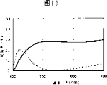
Fig. 5 represents the spectral transmission character of example 1 LCD.
Fig. 6 represents the spectral transmission character of example 2 LCD.
Fig. 7 represents the spectral transmission character of example 3 LCD.
Fig. 8 represents the spectral transmission character of Comparative Examples 1 LCD.
Fig. 9 represents the spectral transmission character of Comparative Examples 2 LCD.
Figure 10 represents the spectral reflectance property of example 4 LCD.
Figure 11 represents the spectral reflectance property of example 5 LCD.
Figure 12 represents the spectral reflectance property of Comparative Examples 3 LCD.
Figure 13 represents the spectral reflectance property of Comparative Examples 4 LCD.
Embodiment
Further describe the present invention with reference to following Example, but the invention is not restricted to this.
Use the test in the liquid crystal indicator execution example, in test from showing that the side transparency carrier counterclockwise and along the pointer direction is defined as "+" and "-" respectively when another transparency carrier is observed.But opposite, even from showing side transparency carrier clockwise direction and counterclockwise be defined as "+" and "-", the actual identical result that obtains respectively when another transparency carrier is observed.
In example, determine the birefringent wavelength dispersion of employed every kind of material in liquid crystal cells and the optical compensatory element by following method.At first, by material preparation level that is used for liquid crystal cells and optical compensatory element and vertical orientated sample.Use Abbe (Abbe) refractometer to measure the birefringence of every kind of sample by the Senarmont method.With the data substitution Cauchy formula that is produced, thereby obtain the wavelength dispersion of material birefringence.
Use above-mentioned formula (10) to measure the delay of each in the employed liquid crystal cells and optical compensatory element in the example.Particularly, use with reference to the described optical anisotropic device of Fig. 1, and incident and exiting side polaroid are arranged to make its absorption axes to satisfy formula (2) and (3) expressed relation as liquid crystal cells and optical compensatory element.Observe transmitted spectrum, find out transmissivity wavelength X min hour,, determine the delay at wavelength X min place then with λ min and torsion angle substitution formula (10).In addition, consider above-mentioned birefringent wavelength dispersion, determine the delay at each wavelength place.
Example 1
The transmission-type STN-LCD that illustrates among preparation Fig. 3.As shown in Figure 3, by a pair ofly face with each other, at interval transparency carrier 31C; Be respectively formed at the electrode 31B on each substrate inside surface; And be printed on respectively on each electrode and constitute liquid crystal cells 31 through the alignment films 31E of orientation process.Liquid crystal material is sealed in by alignment films 31E with by printing and applies in the defined space of sealant 31D that substrate forms on every side, thereby forms liquid crystal material layer 31A.Employed liquid crystal material is the ZLI-2293 that the limited formula of Merck is made.By regulating the direction of orientation of alignment films 31E, liquid crystal material layer 31A is orientated along predetermined direction, thereby makes the molecular orientation windup-degree θ of material
1=+250 degree.The delay R of liquid crystal cells 31 when wavelength X=400nm and λ=550nm
1(400) and R
1(550) be respectively 970nm and 850nm.
Polaroid 33 (SR1862AP that the limited formula of Sumitomo chemistry is made) is arranged on the demonstration side (upside among the figure) of liquid crystal cells 31.Between polaroid 33 and liquid crystal cells 31, constitute optical compensatory element 32 by the liquid crystal polyester liquid crystal film that forms torsion structure.The torsion angle that optical compensatory element 32 has is θ
2=-180 degree.The delay R of optical compensatory element 32 when wavelength X=400nm and λ=550nm
2(400) and R
2(550) be respectively 810nm and 660nm.By changing the mixture ratio of liquid crystal polyester, of the birefringence wavelength chromatic dispersion of control optical compensatory element from big wavelength dispersion value to the small wavelength dispersion values.
As a result, D=0.84.
The rear side of liquid crystal cells when polaroid 34 (SR1862AP that the limited formula of Sumitomo chemistry is made) is arranged on from the observation of demonstration side.Polaroid 33, optical compensatory element 32, liquid crystal cells 31 and polaroid 34 all bond to adjacent component by traditional clear acrylic adhesive bond layer.
Fig. 4 represents the angle θ that defines in each parts of STN-LCD
1, θ
2, θ
A, θ
BAnd θ
CBetween relation.Relation when Fig. 4 represents from the observation of demonstration side between each parts axle orientation.
In Fig. 4, the angle θ that measures to the axis of orientation 321 on optical compensatory element 32 top sides from the absorption axes 331 of polaroid 33
ABe-40 degree; The angle θ that measures to the axis of orientation 311 of liquid crystal cells 31 top sides from the axis of orientation 322 on optical compensatory element 32 bottom sides
BBe-85 degree; And the angle θ that the absorption axes 341 from the axis of orientation 312 on liquid crystal cells 31 bottom sides to polaroid 34 is measured
CBe-45 degree.For the expression of above-mentioned angle, for example θ
ACan be expressed as " θ
A=+140 degree ".But, as mentioned above, select θ
AAbsolute value be the numerical value of 90 degree or littler direction.θ
BAnd θ
CRepresent with same way as.In all the other examples and Comparative Examples, use identical expression.
Driving voltage imposes on the electrode 31B (1/160 dutycycle drives) of liquid crystal indicator under optimal bias from the driving circuit (not shown).The optical property of device in normal black pattern obtains the spectral-transmission characteristics shown in Fig. 5 when checking the use light source.Promptly during non-selection voltage applies, obtain with Comparative Examples 1 in the suitable fabulous black display of employed D-STN pattern; And, during selecting voltage to apply, obtain the more natural and brighter white of tone and show, thereby realize the high-contrast display than D-STN pattern owing to strengthened the long wavelength side transmissivity.But in this example, use the LCD that does not have color filter to test, if use color filter can obtain fabulous polychrome or full color display.When using Transflective sheet (SR1862AS-001 that Sumitomo chemistry company limited makes) when substituting polaroid 34, this display device not only forms good transmission demonstration when using light source, and shows when using the outer light time to form good reflection.
Example 2
Torsion angle except liquid crystal cells 31
1=+250 degree; The delay R of liquid crystal cells 31 when wavelength X=400nm and λ=550nm
1(400) and R
1(550) be respectively 910nm and 800nm; By with the torsion angle of example 1 same procedure by the optical compensatory element 32 of liquid crystal polyester preparation
2=-180 degree; The delay R of liquid crystal compensation element 32 when wavelength X=400nm and λ=550nm
2(400) and R
2(550) be respectively 770nm and 620nm; And θ
A=-40 degree, θ
B=+90 degree and θ
CBeyond=-40 degree, repeat example 1, thereby prepare the LCD similar to example 1.As a result, D=0.78.
Driving voltage imposes on the electrode 31B (1/160 duty cycle drives) of prepared liquid crystal indicator under optimal bias from the driving circuit (not shown).When checking that the use light source is deceived the optical property of pattern lower device often, obtain the spectral transmission character shown in Fig. 6.That is, identical with example 1, during applying, non-selection voltage obtains good black display, and the white that obtains bright and neutralc tint during selecting voltage to apply shows, thereby realizes that high-contrast shows.Though in this example, using does not have the LCD of color filter to test, but if uses color filter can obtain fabulous polychrome or full color demonstration.When using Transflective sheet (SR1862AS-011 that Sumitomo chemistry company limited makes) when substituting polaroid 34, this display device not only forms fabulous transmission demonstration when using light source, and when using the outer light time also to provide good reflection to show.
Example 3
Torsion angle except liquid crystal cells 31
1=+250 degree; The delay R of liquid crystal cells 31 when wavelength X=400nm and λ=550nm
1(400) and R
1(550) be respectively 1025nm and 900nm; By with the torsion angle of example 1 same procedure by the optical compensatory element 32 of liquid crystal polyester preparation
2=-180 degree; The delay R of optical compensatory element 32 when wavelength X=400nm and λ=550nm
2(400) and R
2(550) be respectively 830nm and 700nm; And θ
A=-40 degree, θ
B=+90 degree and θ
CBeyond=-40 degree, repeat example 1, thereby prepare the LCD similar to example 1.As a result, D=0.98.
Driving voltage imposes on the electrode 31B (1/160 duty cycle drives) of prepared liquid crystal indicator under optimal bias from the driving circuit (not shown).When checking that the use light source is deceived the optical property of pattern lower device often, obtain the spectral transmission character shown in Fig. 7.That is, identical with example 1, during applying, non-selection voltage obtains good black display, and the white that obtains bright and neutralc tint during selecting voltage to apply shows, thereby realizes that high-contrast shows.Though in this example, using does not have the LCD of color filter to test, but if uses color filter can obtain fabulous polychrome or full color demonstration.When substituting polaroid 34, this display device of light time forms good reflected image outside using with Transflective sheet (SR1862AU that Sumitomo chemistry company limited makes).
Comparative Examples 1
Except with the compensation liquid crystal cells (not forming electrode on it) that contains the ZLI-2293 that the limited formula of Merck makes of the same preparation of example 1 liquid crystal cells 31, be used for D-STN compensation model compensation liquid crystal cells, and replace optical compensatory element 32; The torsion angle of compensation liquid crystal cells
2=-250 degree; The delay R of compensation liquid crystal cells when wavelength X=400nm and λ=550nm
2(400) and R
2(550) be respectively 910nm and 800nm; And θ
A=+45 degree, θ
B=+90 degree and θ
CBeyond=-45 degree, repeat example 1, thereby prepare the LCD similar to example 1.
Driving voltage imposes on the electrode 31B (1/160 duty cycle drives) of prepared liquid crystal indicator under optimal bias from the driving circuit (not shown).When checking that the use light source is deceived the optical property of pattern lower device often, obtain the spectral transmission character shown in Fig. 8.That is, during non-selection voltage applies, obtain good black image, show thereby obtain high-contrast.But during selecting voltage to apply, prove that the tonal scale 1 of white demonstration is poor.
Comparative Examples 2
Except with the compensation liquid crystal cells (not forming electrode on it) that contains the ZLI-2293 that the limited formula of Merck makes of the same preparation of example 1 liquid crystal cells 31, in order to the compensation liquid crystal cells and replace optical compensatory element 32; The torsion angle of compensation liquid crystal cells
2=-180 degree; And when wavelength X=400nm and λ=550nm the delay R of compensation liquid crystal cells
2(400) and R
2(550) be respectively beyond 750nm and the 660nm, repeat example 1, thereby prepare the LCD similar to example 1.As a result, D=1.16.
Driving voltage imposes on the electrode 31B (1/160 duty cycle drives) of prepared liquid crystal indicator under optimal bias from the driving circuit (not shown).When checking that the use light source is deceived the optical property of pattern lower device often, obtain the spectral transmission character shown in Fig. 9.That is, the effect that realizes with example 1 LCD during non-selection voltage applies is compared, and fully compensation does not show, causes the display contrast low.
Example 4
Torsion angle except liquid crystal cells 31
1=+240 degree; The delay R of liquid crystal cells 31 when wavelength X=400nm and λ=550nm
1(400) and R
1(550) be respectively 910nm and 800nm; The torsion angle of optical compensatory element 32
2=-190 degree; The delay R of optical compensatory element 32 when wavelength X=400nm and λ=550nm
2(400) and R
2(550) be respectively 780nm and 630nm; θ
A=-40 degree, θ
B=+90 degree and θ
C=+45 degree; And replace repeating example 1 beyond the polaroid 34, thereby prepare the LCD similar to example 1 with the polaroid with reflector plate (SR1862AU that Sumitomo chemistry company limited makes).As a result, D=0.76.
Driving voltage imposes on the electrode 31B (1/160 duty cycle drives) of prepared liquid crystal indicator under optimal bias from the driving circuit (not shown).When checking the optical property of normal white mode lower device, obtain the spectral reflectance property shown in Figure 10.That is, during non-selection voltage applies, obtain fabulous blank sheet of paper shape white and show, and during selecting voltage to apply, since lower in the higher 550nm place transmissivity of spectral luminous efficiency, good black display obtained.Thereby realize that high-contrast shows.Though in this example, using does not have the LCD of color filter to test, but if use color filter, can obtain fabulous polychrome or full color and show.When using Transflective sheet (SR1862AS-011 that Sumitomo chemistry company limited makes) when substituting polaroid 34, this display device not only provides good reflection to show, and also provides good transmission to show when the use light source.
Example 5
Torsion angle except liquid crystal cells 31
1=+250 degree; The delay R of liquid crystal cells 31 when wavelength X=400nm and λ=550nm
1(400) and R
1(550) be respectively 970nm and 850nm; The torsion angle of optical compensatory element 32
2=-190 degree; The delay R of optical compensatory element 32 when wavelength X=400nm and λ=550nm
2(400) and R
2(550) be respectively 800nm and 670nm; θ
A=-45 degree, θ
B=+90 degree and θ
C=-45 degree; And substitute beyond the polaroid 34 with reflection type polarizer (Sumitomo 3M company limited make RDF-C), repeat example 1, thereby prepare the LCD similar to example 1.As a result, D=0.94.
Driving voltage imposes on the electrode 31B (1/160 duty cycle drives) of prepared liquid crystal indicator under optimal bias from the driving circuit (not shown).When checking the optical property of normal white mode lower device, obtain the spectral reflectance property shown in Figure 11.That is, during non-selection voltage applies, obtain good blank sheet of paper shape white and show, and during selecting voltage to apply, obtain good black display.Thereby realize that high-contrast shows.Though in this example, using does not have the LCD of color filter to test, but if use color filter, can obtain fabulous polychrome or full color and show.
Comparative Examples 3
Except with the compensation liquid crystal cells (not forming electrode on it) that contains the ZLI-2293 that the limited formula of Merck makes of the same preparation of liquid crystal cells 31, in order to D-STN compensation model compensation liquid crystal cells and replace optical compensatory element 32; The torsion angle of compensation liquid crystal cells
2=-240 degree; The delay R of compensation liquid crystal cells when wavelength X=400nm and λ=550nm
2(400) and R
2(550) be respectively 855nm and 750nm; And θ
A=+45 degree, θ
B=+90 degree and θ
CBeyond=+ 45 degree, repeat example 4, thereby prepare the LCD similar to example 4.
Driving voltage imposes on the electrode 31B (1/160 duty cycle drives) of prepared liquid crystal indicator under optimal bias from the driving circuit (not shown).Check using light source often during the optical property of white mode lower device, obtain the spectral reflectance property shown in Figure 12.That is, when black display, promptly during non-selection voltage applies, at the higher 550nm place of spectral luminous efficiency light taking place and leak, causes the reflective display contrast lower.
Comparative Examples 4
Torsion angle except liquid crystal cells 31
1=+240 degree; The delay R of liquid crystal cells 31 when wavelength X=400nm and λ=550nm
1(400) and R
1(550) be respectively 910nm and 800nm; The torsion angle of optical compensatory element 32
2=-190 degree; And when wavelength X=400nm and λ=550nm the delay R of optical compensatory element
2(400) and R
2(550) be respectively beyond 850nm and the 630nm, repeat example 4, thereby prepare the LCD similar to example 4.As a result, D=0.35.
Driving voltage imposes on the electrode 31B (1/160 duty cycle drives) of prepared liquid crystal indicator under optimal bias from the driving circuit (not shown).Check using light source often during the optical property of white mode lower device, obtain the spectral reflectance property shown in Figure 13.That is, when black display, promptly during selecting voltage to apply, at short wavelength side big light takes place and leak, the display quality that causes obtaining with the liquid crystal indicator of example 4 is compared, and display quality is relatively poor.
Claims (2)
1, a kind of liquid crystal indicator, comprise: liquid crystal cells, this liquid crystal cells is made of a pair of liquid crystal material layer that has the transparency carrier of an electrode respectively and be clipped between the described substrate, be arranged on the polaroid of the both sides of described liquid crystal cells, and be arranged at least one side of described liquid crystal cells and be in optical compensatory element between described liquid crystal cells and the described polaroid, by select voltage from two or more voltages driving voltage is applied on the liquid crystal material layer, the torsion angle of wherein said liquid crystal cells is set at 180 to 270 degree; Described optical compensatory element has the torsion structure that a kind of edge and described liquid crystal cells direction reverse direction reverse; The difference of the torsion angle absolute value of described liquid crystal cells and described optical compensatory element is 40 to 100 degree; The delay difference of stating between liquid crystal cells and the described optical compensatory element in wavelength X=550nm place is 100 to 250nm; And when the absolute value of the delay difference when at wavelength X=400nm and λ=550nm between described liquid crystal cells and described optical compensatory element is used Δ R (400) and Δ R (550) expression respectively, ratio D therebetween is represented as D=Δ R (400)/Δ R (550), and D is in 0.5 to 1.0 scope.
2, liquid crystal indicator according to claim 1, wherein said optical compensatory element are liquid crystal film.
Applications Claiming Priority (2)
| Application Number | Priority Date | Filing Date | Title |
|---|---|---|---|
| JP300757/2001 | 2001-09-28 | ||
| JP2001300757A JP2003107476A (en) | 2001-09-28 | 2001-09-28 | Liquid crystal display element |
Publications (2)
| Publication Number | Publication Date |
|---|---|
| CN1578927A CN1578927A (en) | 2005-02-09 |
| CN1311283C true CN1311283C (en) | 2007-04-18 |
Family
ID=19121285
Family Applications (1)
| Application Number | Title | Priority Date | Filing Date |
|---|---|---|---|
| CNB028214773A Expired - Fee Related CN1311283C (en) | 2001-09-28 | 2002-09-06 | Liquid crystal display |
Country Status (7)
| Country | Link |
|---|---|
| US (1) | US7019804B2 (en) |
| EP (1) | EP1431800B1 (en) |
| JP (1) | JP2003107476A (en) |
| KR (1) | KR100881530B1 (en) |
| CN (1) | CN1311283C (en) |
| DE (1) | DE60230648D1 (en) |
| WO (1) | WO2003029886A1 (en) |
Families Citing this family (19)
| Publication number | Priority date | Publication date | Assignee | Title |
|---|---|---|---|---|
| JP4089631B2 (en) * | 2003-09-16 | 2008-05-28 | ソニー株式会社 | Liquid crystal display device and manufacturing method thereof |
| JP2005141206A (en) * | 2003-10-15 | 2005-06-02 | Nippon Oil Corp | Polymerizable liquid crystalline composition and liquid crystal film produced from the composition |
| JP2005153273A (en) * | 2003-11-25 | 2005-06-16 | Nitto Denko Corp | Resin sheet, liquid crystal cell substrate, liquid crystal display device, substrate for electroluminescence display device, electroluminnescence display device and substrate for solar cell |
| TWI230295B (en) * | 2004-02-06 | 2005-04-01 | Au Optronics Corp | A pixel device of a transflective-type LCD panel |
| CN100363801C (en) * | 2004-05-13 | 2008-01-23 | 统宝光电股份有限公司 | Reflection type twisted column mode liquid crystal display of possessing compensation film |
| JP4640929B2 (en) | 2004-11-09 | 2011-03-02 | 日東電工株式会社 | Liquid crystal display device |
| US7271865B2 (en) * | 2004-12-02 | 2007-09-18 | Research Foundation Of The University Of Central Florida, Inc. | General film compensated reflective twisted nematic liquid crystal display |
| JP2006309105A (en) * | 2005-03-30 | 2006-11-09 | Casio Comput Co Ltd | Liquid crystal display device |
| US20070013843A1 (en) * | 2005-07-12 | 2007-01-18 | Yuuichi Nishikouji | Liquid crystal panel and liquid crystal display using the same |
| US20070013844A1 (en) * | 2005-07-12 | 2007-01-18 | Nitto Denko Corporation | Liquid crystal panel and liquid crystal display using the same |
| JP2007057665A (en) * | 2005-08-23 | 2007-03-08 | Fujifilm Corp | Optical film, image display, and liquid crystal display |
| KR100754390B1 (en) * | 2005-12-08 | 2007-08-31 | 삼성전자주식회사 | Light guide panel and back light unit using the same |
| KR101257929B1 (en) * | 2006-09-20 | 2013-04-24 | 엘지디스플레이 주식회사 | Liquid Crystal Display Panel And Method for Fabricating Thereof |
| EP2137558B1 (en) * | 2007-04-16 | 2011-10-19 | North Carolina State University | Low-twist chiral liquid crystal polarization gratings and related fabrication methods |
| US20130113682A1 (en) * | 2010-10-05 | 2013-05-09 | Stephen D. Heizer | Bidirectional display for a portable electronic device |
| EP2742383B1 (en) * | 2011-08-08 | 2018-01-17 | Merck Patent GmbH | Layer arrangement for the regulation of light transmission |
| CN104062801B (en) * | 2014-06-12 | 2017-01-25 | 京东方科技集团股份有限公司 | Liquid crystal display device and manufacturing method of liquid crystal display device |
| CN104238190A (en) * | 2014-10-20 | 2014-12-24 | 南京华日触控显示科技有限公司 | ASTN liquid crystal display manufactured through chiral liquid crystal delay film and manufacturing method |
| US20210222070A1 (en) * | 2018-06-15 | 2021-07-22 | Compound Photonics U.S. Corporation | Liquid crystal mixtures, methods of making the same, and devices including the same |
Citations (3)
| Publication number | Priority date | Publication date | Assignee | Title |
|---|---|---|---|---|
| JPH0416917A (en) * | 1990-05-11 | 1992-01-21 | Ricoh Co Ltd | Liquid crystal display element |
| US5737046A (en) * | 1995-10-13 | 1998-04-07 | Sharp Kabushiki Kaisha | Birefringence control type liquid crystal display device |
| JP2001228328A (en) * | 2000-02-15 | 2001-08-24 | Nippon Mitsubishi Oil Corp | Reflection type liquid crystal display device |
Family Cites Families (16)
| Publication number | Priority date | Publication date | Assignee | Title |
|---|---|---|---|---|
| JP2537608B2 (en) * | 1986-12-15 | 1996-09-25 | セイコーエプソン株式会社 | Liquid crystal display |
| JP2615715B2 (en) * | 1987-12-10 | 1997-06-04 | セイコーエプソン株式会社 | Manufacturing method of electro-optical element |
| DE69018282T2 (en) | 1989-01-26 | 1995-08-03 | Nippon Oil Co Ltd | Equalizer for a liquid crystal display device. |
| US5280214A (en) * | 1989-10-13 | 1994-01-18 | Ultra Performance International, Inc. | Spark plug with a ground electrode concentrically disposed to a central electrode |
| US5250214A (en) | 1990-04-09 | 1993-10-05 | Ricoh Company, Ltd. | Liquid crystal color display device provided with a color filter film and an optical phase plate comprising liquid crystal polymer |
| JP2585836B2 (en) | 1990-04-19 | 1997-02-26 | 株式会社リコー | Color liquid crystal display device |
| JPH03291620A (en) | 1990-04-10 | 1991-12-20 | Nippon Oil Co Ltd | Compensating plate for liquid crystal display element |
| JPH03291623A (en) | 1990-04-10 | 1991-12-20 | Nippon Oil Co Ltd | Compensating plate for liquid crystal display element |
| JP2687035B2 (en) | 1990-04-13 | 1997-12-08 | 日本石油株式会社 | Manufacturing method of compensator for liquid crystal display element |
| JP3725187B2 (en) * | 1993-09-21 | 2005-12-07 | セイコーエプソン株式会社 | Liquid crystal display device and electronic device |
| KR100241816B1 (en) | 1995-11-24 | 2000-02-01 | 니시무로 타이죠 | Liquid crystal display device and optical isotropic device |
| JP2970541B2 (en) * | 1996-07-16 | 1999-11-02 | 松下電器産業株式会社 | Reflective LCD panel |
| JP3990754B2 (en) * | 1996-10-02 | 2007-10-17 | 旭硝子株式会社 | Reflective monochrome liquid crystal display |
| JP3399795B2 (en) * | 1997-08-28 | 2003-04-21 | シャープ株式会社 | Liquid crystal display |
| JP3921012B2 (en) * | 1999-09-17 | 2007-05-30 | 新日本石油株式会社 | Reflective liquid crystal display element |
| JP2003515190A (en) * | 1999-11-19 | 2003-04-22 | デジマ テック ビー.ヴィ. | Normally white super twisted nematic liquid crystal display |
-
2001
- 2001-09-28 JP JP2001300757A patent/JP2003107476A/en active Pending
-
2002
- 2002-09-06 EP EP02800225A patent/EP1431800B1/en not_active Expired - Fee Related
- 2002-09-06 WO PCT/JP2002/009120 patent/WO2003029886A1/en active Application Filing
- 2002-09-06 US US10/490,709 patent/US7019804B2/en not_active Expired - Fee Related
- 2002-09-06 KR KR1020047004484A patent/KR100881530B1/en not_active IP Right Cessation
- 2002-09-06 DE DE60230648T patent/DE60230648D1/en not_active Expired - Lifetime
- 2002-09-06 CN CNB028214773A patent/CN1311283C/en not_active Expired - Fee Related
Patent Citations (3)
| Publication number | Priority date | Publication date | Assignee | Title |
|---|---|---|---|---|
| JPH0416917A (en) * | 1990-05-11 | 1992-01-21 | Ricoh Co Ltd | Liquid crystal display element |
| US5737046A (en) * | 1995-10-13 | 1998-04-07 | Sharp Kabushiki Kaisha | Birefringence control type liquid crystal display device |
| JP2001228328A (en) * | 2000-02-15 | 2001-08-24 | Nippon Mitsubishi Oil Corp | Reflection type liquid crystal display device |
Also Published As
| Publication number | Publication date |
|---|---|
| DE60230648D1 (en) | 2009-02-12 |
| KR20040037159A (en) | 2004-05-04 |
| JP2003107476A (en) | 2003-04-09 |
| EP1431800A4 (en) | 2006-08-02 |
| CN1578927A (en) | 2005-02-09 |
| EP1431800B1 (en) | 2008-12-31 |
| KR100881530B1 (en) | 2009-02-05 |
| US7019804B2 (en) | 2006-03-28 |
| WO2003029886A1 (en) | 2003-04-10 |
| EP1431800A1 (en) | 2004-06-23 |
| US20040246418A1 (en) | 2004-12-09 |
Similar Documents
| Publication | Publication Date | Title |
|---|---|---|
| CN1311283C (en) | Liquid crystal display | |
| KR100849300B1 (en) | Circular polarization plate and liquid crystal display device | |
| JP5311605B2 (en) | Liquid crystal panel and liquid crystal display device | |
| CN1235071C (en) | Circular polarization plate and liquid crystal display | |
| CN1041967C (en) | Liquid crystal display element and laminated retardation film applied thereto | |
| CN1806192A (en) | Complex light-compensation C plate with two or more of C plates different in dispersion ratio value and liquid crystal display using the same | |
| TWI396009B (en) | Transmissive liquid crystal display device | |
| TWI413810B (en) | Transmissive liquid crystal display device | |
| CN1129808C (en) | Liquid crystal display | |
| CN1815309A (en) | Liquid crystal display and electronic apparatus | |
| CN1745331A (en) | Bi-axial retardation compensation film and vertically aligned liquid crystal display using the same | |
| CN1289955C (en) | Translucent reflective liquid crystal display | |
| JP2015036735A (en) | Optical film, polarizing plate, and liquid crystal display device | |
| WO2004031846A1 (en) | Semitransmissive reflective liquid crystal display element | |
| CN1247326A (en) | Reflecting liquid crystal displaying components | |
| CN1128383C (en) | Reflection liquid crystal display element | |
| CN1127672C (en) | Reflection liquid crystal display device | |
| CN1729505A (en) | Liquid crystal display device with reduced power consumption in standby mode | |
| JPH09197388A (en) | Reflection type liquid crystal display device | |
| CN1223383A (en) | Reflection type liquid crystal display element | |
| JP2002148611A (en) | Semitransmission type liquid crystal display device | |
| JP4181261B2 (en) | Reflective liquid crystal display | |
| JP2891227B2 (en) | Liquid crystal device | |
| JP2947206B2 (en) | Liquid crystal device | |
| JP2947207B2 (en) | Liquid crystal device |
Legal Events
| Date | Code | Title | Description |
|---|---|---|---|
| C06 | Publication | ||
| PB01 | Publication | ||
| C10 | Entry into substantive examination | ||
| SE01 | Entry into force of request for substantive examination | ||
| C14 | Grant of patent or utility model | ||
| GR01 | Patent grant | ||
| C17 | Cessation of patent right | ||
| CF01 | Termination of patent right due to non-payment of annual fee |
Granted publication date: 20070418 Termination date: 20120906 |