CN1300837C - Semiconductor device mfg. method - Google Patents
Semiconductor device mfg. method Download PDFInfo
- Publication number
- CN1300837C CN1300837C CNB03101674XA CN03101674A CN1300837C CN 1300837 C CN1300837 C CN 1300837C CN B03101674X A CNB03101674X A CN B03101674XA CN 03101674 A CN03101674 A CN 03101674A CN 1300837 C CN1300837 C CN 1300837C
- Authority
- CN
- China
- Prior art keywords
- interlayer dielectric
- film
- manufacture method
- during
- semiconductor device
- Prior art date
- Legal status (The legal status is an assumption and is not a legal conclusion. Google has not performed a legal analysis and makes no representation as to the accuracy of the status listed.)
- Expired - Fee Related
Links
Images


Classifications
-
- H—ELECTRICITY
- H10—SEMICONDUCTOR DEVICES; ELECTRIC SOLID-STATE DEVICES NOT OTHERWISE PROVIDED FOR
- H10B—ELECTRONIC MEMORY DEVICES
- H10B12/00—Dynamic random access memory [DRAM] devices
- H10B12/01—Manufacture or treatment
- H10B12/02—Manufacture or treatment for one transistor one-capacitor [1T-1C] memory cells
- H10B12/03—Making the capacitor or connections thereto
- H10B12/033—Making the capacitor or connections thereto the capacitor extending over the transistor
-
- H—ELECTRICITY
- H01—ELECTRIC ELEMENTS
- H01L—SEMICONDUCTOR DEVICES NOT COVERED BY CLASS H10
- H01L21/00—Processes or apparatus adapted for the manufacture or treatment of semiconductor or solid state devices or of parts thereof
- H01L21/70—Manufacture or treatment of devices consisting of a plurality of solid state components formed in or on a common substrate or of parts thereof; Manufacture of integrated circuit devices or of parts thereof
- H01L21/71—Manufacture of specific parts of devices defined in group H01L21/70
- H01L21/768—Applying interconnections to be used for carrying current between separate components within a device comprising conductors and dielectrics
- H01L21/76801—Applying interconnections to be used for carrying current between separate components within a device comprising conductors and dielectrics characterised by the formation and the after-treatment of the dielectrics, e.g. smoothing
- H01L21/76822—Modification of the material of dielectric layers, e.g. grading, after-treatment to improve the stability of the layers, to increase their density etc.
- H01L21/76828—Modification of the material of dielectric layers, e.g. grading, after-treatment to improve the stability of the layers, to increase their density etc. thermal treatment
-
- H—ELECTRICITY
- H01—ELECTRIC ELEMENTS
- H01L—SEMICONDUCTOR DEVICES NOT COVERED BY CLASS H10
- H01L21/00—Processes or apparatus adapted for the manufacture or treatment of semiconductor or solid state devices or of parts thereof
- H01L21/70—Manufacture or treatment of devices consisting of a plurality of solid state components formed in or on a common substrate or of parts thereof; Manufacture of integrated circuit devices or of parts thereof
- H01L21/71—Manufacture of specific parts of devices defined in group H01L21/70
- H01L21/768—Applying interconnections to be used for carrying current between separate components within a device comprising conductors and dielectrics
- H01L21/76838—Applying interconnections to be used for carrying current between separate components within a device comprising conductors and dielectrics characterised by the formation and the after-treatment of the conductors
-
- H—ELECTRICITY
- H10—SEMICONDUCTOR DEVICES; ELECTRIC SOLID-STATE DEVICES NOT OTHERWISE PROVIDED FOR
- H10B—ELECTRONIC MEMORY DEVICES
- H10B12/00—Dynamic random access memory [DRAM] devices
- H10B12/30—DRAM devices comprising one-transistor - one-capacitor [1T-1C] memory cells
- H10B12/31—DRAM devices comprising one-transistor - one-capacitor [1T-1C] memory cells having a storage electrode stacked over the transistor
-
- H—ELECTRICITY
- H10—SEMICONDUCTOR DEVICES; ELECTRIC SOLID-STATE DEVICES NOT OTHERWISE PROVIDED FOR
- H10B—ELECTRONIC MEMORY DEVICES
- H10B53/00—Ferroelectric RAM [FeRAM] devices comprising ferroelectric memory capacitors
-
- H—ELECTRICITY
- H10—SEMICONDUCTOR DEVICES; ELECTRIC SOLID-STATE DEVICES NOT OTHERWISE PROVIDED FOR
- H10B—ELECTRONIC MEMORY DEVICES
- H10B53/00—Ferroelectric RAM [FeRAM] devices comprising ferroelectric memory capacitors
- H10B53/30—Ferroelectric RAM [FeRAM] devices comprising ferroelectric memory capacitors characterised by the memory core region
Abstract
The invention can prevent a capacitor insulating film containing a ferromagnetic material of a metal oxide body from deteriorating its electrical properties due to the moisture discharged from an interlayer insulating film through a thermal treatment. A capacitor element 108 containing a capacitor insulating film 106 of a metal oxide is formed on a board 101. Then, an interlayer insulating film 109A of silicon oxide is deposited on the capacitor element 108, and then a barrier film 110B electrically connected to the capacitor element 108 is formed on the interlayer insulating film 109A. When the board 101 where the barrier film 110B is formed is transferred in an after process, the board 101 where the interlayer insulating film 109A is exposed is housed in a quartz housing case 20 whose inside is hermetically sealed up so as to be kept lower in moisture content with a moisture absorbent than the outside in a transfer time or a standby time necessary before or after it is transferred.
Description
Technical field
The present invention relates to be included in the capacitor insulating film manufacture method of the semiconductor device of the capacity cell that uses the strong dielectric that constitutes by metal oxide or high dielectric.
Background technology
In capacitor insulating film, has the capacity cell of the strong dielectric film that constitutes by metal oxide or high dielectric film because have based on the remnant polarization of hysteresis characteristic and high dielectric constant, so in the field of Nonvolatile memory devices or DRAM device, substituting capacity cell in the past with the capacitor insulating film that constitutes by silica or silicon nitride.
But, when a Semiconductor substrate (wafer) goes up the formation capacity cell, must be through a plurality of manufacturing steps, during during the conveying of usually carrying between a plurality of manufacturing installations or before carrying or in during the standby after carrying, the Semiconductor substrate in the manufacturing is stored in the reservoir vessel by moldable resin material (plastics) formation.
The inventor has found following problem points in the manufacture method of the described semiconductor device that comprises the capacity cell that is made of strong dielectric film or high dielectric film in the past.
Promptly be arranged on capacity cell on the Semiconductor substrate and the interlayer dielectric between the wiring layer from a step during the conveying of then other steps of this step or during the standby, absorb the moisture of gas medium, the moisture of absorption worsens the electrical characteristics of capacitor insulating film.Below, its main cause is described.
Figure 11 has represented the remnant polarization value of the capacity cell with the capacitor insulating film that is made of strong dielectric in the past and each annealing temperature dependence of withstand voltage.At this, on capacity cell, form wiring, forming by ozone (O
3) and TEOS (tetraethyl orthosilicate) under normal pressure, react and behind the interlayer dielectric that the silica (ozone TEOS) that obtains constitutes, in the oxygen gas medium, 300 ℃, 350 ℃ and 400 ℃ at each temperature, carried out annealing in process.
As can be seen from Figure 11, if carry out annealing in process under 400 ℃ temperature, then remnant polarization value and withstand voltage all worsen.
In addition, Figure 12 has represented based on the heating-up temperature dependence that heat up to break away from moisture concentration gas analysis (Thermal DesorptionSpectroscopy:TDS) method, that emit from silica.As can be seen from Figure 12,, just can observe the moisture of emitting from silica if the heating-up temperature of Semiconductor substrate is become more than 200 ℃, irrelevant with underlayer temperature, at 400 ℃ of peak values with moisture concentration.
As previously discussed, the interlayer dielectric that is made of ozone TEOS absorbs the moisture in the gas medium during carrying or in during the standby, because the moisture that is absorbed breaks away from easily, so the annealing in process by thereafter, the moisture of this absorption and strong dielectric reaction descend remnant polarization value.
But, on the other hand, on the basis of rate of finished products that improves semiconductor device and reliability,, be necessary to carry out annealing in process high temperature under and the formation processing of diaphragm in order to form the injury recovery after the wiring and to prevent the corrosion of aluminium.
Summary of the invention
The existence of problem in view of the above the objective of the invention is to: make the electrical characteristics of the capacitor insulating film that comprises the strong dielectric that is made of metal oxide can be owing to the moisture of emitting from interlayer dielectric by heat treatment worsens.
In order to realize above-described purpose, the present invention is in the manufacture method of the semiconductor device with the capacity cell that comprises the capacitor insulating film that is made of metal oxide, adopted during the conveying of next step or in during the standby, made the moisture free structure of the interlayer dielectric that constitutes by oxide.
Specifically, the manufacture method of first semiconductor device of the present invention comprises: the first step that forms the capacity cell that comprises the capacitor insulating film that is made of metal oxide on substrate; On capacity cell, deposit second step of the interlayer dielectric that constitutes by oxide; After the zone above the capacity cell on the interlayer dielectric is provided with peristome, on interlayer dielectric, form the conductive film that has connected capacity cell by peristome, the third step that the upper section of the periphery of the capacity cell in the interlayer dielectric is exposed; During during the conveying when promptly the 4th step is carried the step of substrate after third step that has formed conductive film or before carrying or in during the standby after carrying, in during before almost whole of the surface of interlayer dielectric covered by other members, the substrate stores that has formed conductive film in the low reservoir vessel of the moisture concentration of moisture concentration outside gas medium of gas inside medium than it.
Manufacture method according to first semiconductor device, because during carrying or in during the standby, be formed on the amount of moisture reduction that the interlayer dielectric on the substrate absorbs from atmosphere, even so after step in when having comprised annealing in process, also be difficult to emit moisture, so can prevent to be reduced the deterioration of the electrical characteristics of the capacitor insulating film that produces owing to the capacitor insulating film that comprises the strong dielectric that constitutes by metal oxide etc. from the interlayer dielectric of heating.
In the manufacture method of first semiconductor device, third step preferably forms the step of the barrier film that is made of conductive film.
At this moment, the 4th step preferably deposits the step that other members promptly are used to form the wiring formation film of wiring on whole that comprises on the interlayer dielectric of conductive film.
In addition, in the manufacture method of first semiconductor device, third step preferably forms the step of the wiring that is made of conductive film.
The manufacture method of first semiconductor device is preferably in after the 4th step, also has for conductive film the 5th step of heat-treating under about temperature more than 200 ℃.The annealing in process of the injury recovery after like this, the pattern that can be used for capacitor insulating film or conductive film reliably forms.
In the manufacture method of first semiconductor device, interlayer dielectric preferably is made of silica.
In the manufacture method of first semiconductor device, conductive film preferably is made of any one monofilm formed in titanium, titanium nitride, aluminium, tungsten and the copper or two kinds stacked film comprising in them at least.
The manufacture method of second semiconductor device of the present invention comprises: the first step that forms the capacity cell that comprises the capacitor insulating film that is made of metal oxide on substrate; On capacity cell, form second step of first interlayer dielectric; On first interlayer dielectric, form the third step of first conductive film that has been electrically connected capacity cell; Comprising the 4th step that forms second interlayer dielectric that constitutes by oxide on first interlayer dielectric of first conductive film; On almost whole on second interlayer dielectric, form the 5th step of second conductive film; The substrate that has formed second interlayer dielectric during the conveying of the 4th step when the 5th step is carried or before carrying during or during the standby after the conveying, the substrate stores that has formed second interlayer dielectric in the low reservoir vessel of the moisture concentration of moisture concentration outside gas medium of gas inside medium than it.
Manufacture method according to second semiconductor device, because during carrying or in during the standby, be formed on the amount of moisture reduction that second interlayer dielectric on the substrate absorbs from atmosphere, even so after step in when having comprised annealing in process, also be difficult to emit moisture, can prevent to be reduced the deterioration of the electrical characteristics of the capacitor insulating film that produces owing to the capacitor insulating film that comprises the strong dielectric that constitutes by metal oxide etc. from second interlayer dielectric of heating.
The manufacture method of second semiconductor device also has for second conductive film after the 5th step, the 6th step of heat-treating under about temperature more than 200 ℃.
In the manufacture method of second semiconductor device, first interlayer dielectric or second interlayer dielectric preferably are made of silica.
In the manufacture method of second semiconductor device, first conductive film and second conductive film are made of any one monofilm formed in titanium, titanium nitride, aluminium, tungsten and the copper or two kinds stacked film comprising in them at least.
The manufacture method of the 3rd semiconductor device of the present invention comprises: the first step that forms the capacity cell that comprises the capacitor insulating film that is made of metal oxide on substrate; On capacity cell, deposit second step of the interlayer dielectric that constitutes by oxide; On interlayer dielectric, form the third step of the wiring that constitutes by conductive film; On almost whole that comprises on the described interlayer dielectric of wiring, form the 4th step of the diaphragm that constitutes by nitride; The substrate that has formed interlayer dielectric and wiring during the conveying of third step when the 4th step is carried or before carrying during or during the standby after the conveying, the substrate stores that has formed interlayer dielectric and wiring in the low reservoir vessel of the moisture concentration of moisture concentration outside gas medium of gas inside medium than it.
Manufacture method according to the 3rd semiconductor device, because during carrying or in during the standby, be formed on the amount of moisture reduction that the interlayer dielectric on the substrate absorbs from atmosphere, even so after step in when having comprised annealing in process, also be difficult to emit moisture, so can prevent to be reduced the deterioration of the electrical characteristics of the capacitor insulating film that produces owing to the capacitor insulating film that comprises the strong dielectric that constitutes by metal oxide etc. from the interlayer dielectric of heating.
The manufacture method of the 3rd semiconductor device preferably also has for wiring step of heat treatment under about temperature more than 200 ℃ between third step and the 4th step.
In the manufacture method of the 3rd semiconductor device, interlayer dielectric preferably is made of silica.
In the manufacture method of the 3rd semiconductor device, diaphragm preferably is made of silicon nitride.
In the manufacture method of the 3rd semiconductor device, conductive film is made of any one monofilm formed in titanium, titanium nitride, aluminium, tungsten and the copper or two kinds stacked film comprising in them at least.
The manufacture method of the 4th semiconductor device of the present invention comprises: the step that forms the capacity cell that comprises the capacitor insulating film that is made of metal oxide on substrate; During during the conveying when the step of the substrate that has formed capacity cell after the step that forms capacity cell carried or before carrying or in during the standby after the conveying, the substrate stores that has formed capacity cell in the low reservoir vessel of the moisture concentration of moisture concentration outside gas medium of gas inside medium than it.
According to the manufacture method of the 4th semiconductor device, though after step in when having comprised annealing in process, the deterioration of the electrical characteristics of the capacitor insulating film that the capacitor insulating film that also can prevent to comprise strong dielectric of being made of metal oxide etc. produces owing to moisture.
In the manufacture method of first~the 4th semiconductor device, reservoir vessel is preferably formed as to salable, and portion has dropped into hygroscopic material within it.
At this moment, hygroscopic material preferably is made of silica gel or activated alumina.
In addition, in the manufacture method of first~the 4th semiconductor device, reservoir vessel is preferably formed as to salable, and portion has filled inert gas or kept vacuum within it.
At this moment, inert gas preferably is made of nitrogen, argon or helium.
In the manufacture method of first~the 4th semiconductor device, metal oxide is preferably the layer structure perovskite composite oxide that comprises bismuth or comprises lead, zirconium and titanium or the perovskite composite oxide of strontium and titanium.
Description of drawings
Following brief description accompanying drawing.
Fig. 1 (a)~(c) is the mode configuration cutaway view of sequence of steps of the manufacturing method for semiconductor device of the expression embodiment of the invention 1.
Fig. 2 (a)~(c) is the mode configuration cutaway view of sequence of steps of the manufacturing method for semiconductor device of the expression embodiment of the invention 1.
Fig. 3 is the mode configuration cutaway view of a step of manufacture method of semiconductor device of a variation of the expression embodiment of the invention 1.
Fig. 4 (a)~(c) is the mode configuration cutaway view of sequence of steps of the manufacturing method for semiconductor device of the expression embodiment of the invention 2.
Fig. 5 (a)~(c) is the mode configuration cutaway view of sequence of steps of the manufacturing method for semiconductor device of the expression embodiment of the invention 2.
Fig. 6 (a) and (b) be the mode configuration cutaway view of sequence of steps of the manufacturing method for semiconductor device of the expression embodiment of the invention 2.
Fig. 7 (a) and (b) be the mode configuration cutaway view of sequence of steps of manufacturing method for semiconductor device of a variation of the expression embodiment of the invention 2.
Fig. 8 (a)~(c) is the mode configuration cutaway view of sequence of steps of the manufacturing method for semiconductor device of the expression embodiment of the invention 3.
Fig. 9 (a) and (b) be the mode configuration cutaway view of sequence of steps of the manufacturing method for semiconductor device of the expression embodiment of the invention 3.
Figure 10 is the mode configuration cutaway view of a step of manufacture method of semiconductor device of a variation of the expression embodiment of the invention 3.
Figure 11 represents the remnant polarization value of the capacity cell with the capacitor insulating film that is made of strong dielectric in the past and the dependent curve chart of each annealing temperature of withstand voltage.
Figure 12 is expression based on the dependent curve chart of heating-up temperature that heat up to break away from moisture concentration eudiometry, that emit from silica.
Following brief description reference numeral.
10-the first reservoir vessel; 10a-container body portion; 10b-cap; 20-the second reservoir vessel; 20a-container body portion; 20b-cap; 21-hygroscopic material; 30-the three reservoir vessel; 30a-container body portion; 30b-cap; 101-wafer (Semiconductor substrate); 102-element separated region; 103-MOS transistor; 103a-gate electrode; 103b-source region; 103c-drain region; 104-the first interlayer dielectric; 105-lower electrode; 106-capacitor insulating film; 107-upper electrode; 108-capacity cell; 109A-second interlayer dielectric (PSG); 109B-second interlayer dielectric (silica); 109a-first contact hole; 109b-second contact hole; 110A-stop formation film; 110B-barrier film; 111A-(first) wiring forms film; 111B-(first) wiring; 112-diaphragm; 113-the three interlayer dielectric (ozone TEOS); 113a-the 3rd contact hole; 114A-second wiring forms film; 114B-second wiring.
Embodiment
(embodiment 1)
The manufacture method of the semiconductor device of the embodiment of the invention 1 is described with reference to the accompanying drawings.
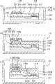
Fig. 1 (a)~Fig. 1 (c) and Fig. 2 (a)~Fig. 2 (c) has represented the pattern cross section structure of sequence of steps of the manufacturing method for semiconductor device that comprises the capacity cell with the capacitor insulating film that is made of strong dielectric of the embodiment of the invention 1.
[the formation step of capacity cell]
Below, the formation step of the capacity cell shown in the key diagram 1 (a).
At first, in the transistorized formation step of the preceding step of the formation step of capacity cell, on the wafer (Semiconductor substrate) 101 that for example constitutes, form the element separated region 102 that constitutes by LOCOS film etc. selectively by silicon (Si).Then, in the element-forming region of dividing of wafer 101, form the MOS transistor 103 that constitutes by gate electrode 103a, source region 103b and drain region 103c by element separated region 102.Then,, on wafer 101, comprising on element separated region 102 and MOS transistor 103 whole for example by the chemical vapor deposition (CVD) method, the about 1500nm of deposition thickness by silica (SiO
2) first interlayer dielectric 104 that constitutes.Then, coating (rotary plating) erosion resistant on the concavo-convex surface of the formation of first interlayer dielectric 104, by carrying out reverse etching for first interlayer dielectric 104 is the reverse etching of so-called resist, makes the flattening surface of first interlayer dielectric 104.
Then, for example by sputtering method, in planarization first interlayer dielectric 104 on the lower electrode of the about 200nm of deposition thickness by platinum (Pt) formation form film.Then, for example by the CVD method, form the strong dielectric film by the metal oxide formation that comprises strontium (Sr), bismuth (Bi) and tantalum (Ta) that deposits the about 200nm of thickness on the film at lower electrode, the upper electrode that is made of platinum (Pt) of the about 200nm of deposition thickness forms film on strong dielectric film once more.Then, by photoetching process and dry ecthing method, carry out pattern selectively and form by successively upper electrode being formed upper section that film, strong dielectric film and lower electrode form the element separated region 102 of film, form film from lower electrode and form lower electrode 105, form capacitor insulating film 106 from strong dielectric film, form film from upper electrode and form upper electrode 107.In view of the above, obtain the capacity cell 108 that constitutes by lower electrode 105, capacitor insulating film 106 and upper electrode 107.It should be noted that, at this for convenience, shown on wafer 101, to form a MOS transistor 103 and a capacity cell 108, but on wafer 101, formed a plurality of MOS transistor 103 and a plurality of capacity cell 108 respectively.Then, carrying out based on temperature for capacity cell 108 is the annealing based on the oxygen gas medium about 800 ℃, the injury recovery that makes the dry ecthing owing to capacity cell film at 108 quarter the time allow capacitor insulating film 106 be subjected to.Then, formed during the conveying before the manufacturing installation of wafer 101 step afterwards of capacity cell 108 or before carrying during or carry after standby during in, be stored in the gas medium (atmosphere) of external container fully blocking be in unsealed first reservoir vessel 10 in the past that constitutes by moldable resin material (plastics).At this, first reservoir vessel 10 is made of 10a of container body portion and cap 10b.
It should be noted that, generally in the formation step of capacity cell, comprise various treatment steps, during the conveying between these treatment steps or in during the standby, also need not non-use reservoir vessel of the present invention, also can use first reservoir vessel 10 in the past.
[stopping the deposition step that forms film]
Then, in stopping the deposition step that forms film, after the wafer 101 that has formed capacity cell 108 taken out from first reservoir vessel 10, shown in Fig. 1 (b), by the atmospheric pressure cvd method, comprising on first interlayer dielectric 104 of capacity cell 108 the second interlayer dielectric 109A of the about 500nm of deposition thickness by silica (PSG) formation that comprises the phosphorus (P) about 5%.Then, by photoetching process and dry ecthing method, form the first contact hole 109a at the upper portion of the upper electrode 107 of the capacity cell 108 of the second interlayer dielectric 109A.Then, by annealing in the oxygen gas medium about 800 ℃, the injury recovery that damage that the hydrogen ion that capacitor insulating film 106 is produced from the deposition of the second interlayer dielectric 109A is subjected to and the dry ecthing during from the formation of the first contact hole 109a are subjected to.Then, by for example sputtering method, deposition thickness about 50nm's forms film 110A by stopping of titanium nitride (TiN) formation on the second interlayer dielectric 109A of bottom surface that comprises the first contact hole 109a and side.Stop that having deposited the wafer 101 that forms film 110A is stored in first reservoir vessel 10, is transported to next step then.
It should be noted that, various treatment steps generally in stopping the deposition step that forms film, have been comprised, during the conveying between these treatment steps or in during the standby, also need not non-use reservoir vessel of the present invention, also can use first reservoir vessel 10 in the past.
[the formation step of barrier film]
Then; in the formation step of barrier film; stop that having deposited the wafer 101 that forms film 110A is after 10 taking-ups of first reservoir vessel; shown in Fig. 1 (c); for stopping that forming film 110A forms by pattern; the part that comprises the first contact hole 109a is stayed, from stopping that forming film 110A forms the barrier film 110B that is electrically connected and protects capacitor insulating film 106 with upper electrode 107.Then, the wafer 101 that has formed the second interlayer dielectric 109A and barrier film 110B is stored in second reservoir vessel 20.At this, second reservoir vessel 20 after the storage of wafer 101, makes the contact-making surface of 20a of container body portion and cap 20b be close to by vacuum grease by forming constituting by forming the 20a of container body portion and the cap 20b that form of sealing, the blocking atmosphere.Also in the inside of second reservoir vessel 20, store by comprising 70% hole and the silica gel of the dry about 100g of weight constitutes under about 1200 ℃ temperature hygroscopic material 21, be transported to next step.
It should be noted that, various treatment steps have been comprised in the formation step of general barrier film, during the conveying between these treatment steps or in during the standby, be that barrier film 110B is carved film, after expose on the surface of the second interlayer dielectric 109A, be necessary in second reservoir vessel 20 of the present invention, to store wafer 101.
[wiring forms the deposition step of film]
Then, form in the deposition step of film in wiring, from second reservoir vessel 20 take out formed the wafer 101 of barrier film 110B after, shown in Fig. 2 (a), by photoetching process and dry ecthing method, form the second contact hole 109b at the upper section of the source region 103b of the MOS transistor 103 of first interlayer dielectric 104 and the second interlayer dielectric 109A.Then, pass through sputtering method, on the second interlayer dielectric 109A, on bottom surface that comprises the second contact hole 109b and the side and on whole of barrier film 110B, the titanium nitride (TiN) of the aluminium (Al) of the titanium nitride (TiN) of the titanium of the about 20nm of deposit thickness (Ti), the about 100nm of thickness, the about 700nm of thickness and the about 50nm of thickness successively, the wiring of the four-layer structure that has formed metal film and metal nitride film stacked forms film 111A.Then, the wafer 101 that has deposited wiring formation film 111A is stored in first reservoir vessel 10, is transported to next step.
It should be noted that, the deposition step that general wiring forms film has comprised various treatment steps, during the conveying between these treatment steps or in during the standby, promptly before the deposition that wiring forms film 111A finishes during in, be necessary in second reservoir vessel 20 of the present invention, to store wafer 101.
[the formation step of wiring]
Then, in the formation step of wiring, from first reservoir vessel 10 taken out having deposited the wafer 101 that wiring forms film 111A after, shown in Fig. 2 (b), by dry ecthing, by comprising the first contact hole 109a and the second contact hole 109b, wiring is formed film 111A carve film, form film 111A from this wiring and form wiring 111B.Then, by in the about 450 ℃ oxygen gas medium of temperature, annealing, make capacitor insulating film 106 recover when wiring forms the deposition of film 111A and damage that pattern is subjected to when forming.By this annealing in process, form the residual chlorine volatilization of using in the etching gas of dry ecthing of film 111A for wiring, so can prevent to constitute the corrosion of the aluminium of wiring 111B.Then the wafer 101 that has formed wiring 111B is stored in first reservoir vessel 10, is transported to next step.
It should be noted that, generally in the formation step of wiring, comprised various treatment steps, during the conveying between these treatment steps or in during the standby, also need not non-use reservoir vessel of the present invention, also can use first reservoir vessel 10 in the past.
[deposition step of diaphragm]
Then; in the deposition step of diaphragm; after taking out the wafer 101 that has formed wiring 111B from first reservoir vessel 10; shown in Fig. 2 (c); for example by being raw material with silane; and underlayer temperature is about 400 ℃ plasma CVD method, on the second interlayer dielectric 109A that comprises the 111B that connects up, and protection (passivation) film 112 that constitutes by silicon nitride of deposition thickness about 800nm on whole.Then, the wafer that has deposited diaphragm 112 is stored in first reservoir vessel 10, is transported to next step.Then, though show among the figure, in next step, in the desirable pad of diaphragm 112 formation portion.
It should be noted that, comprised various treatment steps in the deposition step of general diaphragm, during the conveying between these treatment steps or in during the standby, also need not non-use reservoir vessel of the present invention, also can use first reservoir vessel 10 in the past.
More than, according to embodiment 1, shown in Fig. 1 (c), from the formation step of barrier film during wiring forms the conveying that the deposition step of film carries or before carrying during or during the standby after the conveying, wafer 101 is stored in inside and has collected hygroscopic material 21 and be set in sealable second reservoir vessel 20, so in during before deposition wiring forms film 111A, the exposed portions serve of the second interlayer dielectric 109A that is made of silica is not exposed in the atmosphere.Therefore, during the conveying of wafer 101 or in during the standby, can suppress the hygroscopic effect of the second interlayer dielectric 109A.In view of the above, during the annealing in process of oxygen gas medium of the about 450 ℃ temperature in the formation step of wiring, can reduce the damage that the capacitor insulating film 106 of capacity cell 108 is subjected to owing to the moisture of emitting from the second interlayer dielectric 109A.
It should be noted that, use second reservoir vessel 20 during be not limited to barrier film formation step and wiring form between the deposition step of film, in other steps with also using.
But, from the formation step of barrier film forms conveying the deposition step of film to wiring during or during the standby, because use second reservoir vessel 20 that has stored hygroscopic material 21 and sealing, so compared with the past, the withstand voltage of capacity cell 108 of embodiment 1 increases to 20V from 15V.In addition, preservation characteristics has also increased an order of magnitude.
(variation of embodiment 1)
Below, with reference to accompanying drawing, the manufacture method of semiconductor device of a variation of the embodiment of the invention 1 is described.
Fig. 3 has represented the pattern cross section structure of a step of manufacture method of the semiconductor device that comprises the capacity cell with the capacitor insulating film that is made of strong dielectric of a variation of the embodiment of the invention 1.At this, the difference with embodiment 1 only is described.In Fig. 3,, omitted explanation by the member of formation identical with the member of formation shown in Fig. 1 (c) adopted identical symbol.
[the formation step of barrier film]
As shown in Figure 3; from first reservoir vessel 10 taken out deposited stop the wafer 101 that forms film 110A after; by to stopping that forming film 110A carries out pattern and form; make the part that comprises the first contact hole 109a residual, from stopping that forming film 110A forms the barrier film 110B that is electrically connected and protects capacitor insulating film 106 with upper electrode 107.Then, the wafer 101 that has formed the second interlayer dielectric 109A and barrier film 110B is stored in the 3rd reservoir vessel 30, constitute by sealable 30a of container body portion and the cap 30b that forms by aluminium at this 3rd reservoir vessel 30, though do not show among the figure, the additional gas that is provided with injects valve and drain tap in the 30a of container body portion.After the storage of wafer 101, the gas inside medium of the 3rd reservoir vessel 30 be replaced into pressure 700 * 133.32Pa (=700Torr) be in a ratio of the nitrogen (N of decompression state with atmosphere
2).The contact-making surface of 30a of container body portion and cap 30b is close to by having applied vacuum grease, and is salable.The wiring that is transported to next step then forms the deposition step of film.
Like this, according to this variation, during the conveying the deposition step that forms film from the formation step of barrier film to wiring or during the standby, used the 3rd reservoir vessel 30 of having filled nitrogen in inside, so the exposed portions serve of the second interlayer dielectric 109A that is made of silica can not be exposed in the atmosphere.Therefore, the withstand voltage of capacity cell 108 of this variation increases to 22V from 15V, and its retention performance has also increased by two orders of magnitude.
Like this, during the annealing in process of the oxygen gas medium of the about 450 ℃ temperature in the formation step of wiring, can reduce because the damage that the capacitor insulating film 106 that the moisture that the second interlayer dielectric 109A emits causes is subjected to.
It should be noted that, in the formation step of barrier film, various treatment steps have been comprised, but after forming barrier film 110B to the deposition wiring form during the conveying between various treatment steps the film 111A or during the standby, be necessary wafer is stored in the 3rd reservoir vessel 30.
(embodiment 2)
Below, with reference to accompanying drawing, the manufacture method of the semiconductor device of the embodiment of the invention 2 is described.
Fig. 4 (a)~Fig. 4 (c) has represented the pattern cross section structure of sequence of steps of the manufacturing method for semiconductor device that comprises the capacity cell with the capacitor insulating film that is made of strong dielectric of the embodiment of the invention 2 to Fig. 6 (a) and Fig. 6 (b).In embodiment 2, the member of formation identical with the member of formation shown in the embodiment 1 adopted identical symbol.
[the formation step of capacity cell]
Below, the formation step of the capacity cell shown in the key diagram 4 (a).
At first, in the transistorized formation step of the preceding step of the formation step of capacity cell, for example on the wafer 101 that constitutes by silicon, form the element separated region 102 that constitutes by LOCOS film etc. selectively.Then, in the element-forming region of dividing of wafer 101, form the MOS transistor 103 that constitutes by gate electrode 103a, source region 103b and drain region 103c by element separated region 102.Then, by for example CVD method, on wafer 101, comprising first interlayer dielectric 104 that constitutes by silica of the about 1500nm of deposition thickness on element separated region 102 and MOS transistor 103 whole.Then, on the concavo-convex surface of the formation of first interlayer dielectric 104, apply erosion resistant,, make the flattening surface of first interlayer dielectric 104 by carrying out the reverse etching of resist for first interlayer dielectric 104.
Then, for example by sputtering method, in planarization first interlayer dielectric 104 on the lower electrode that constitutes by platinum of the about 200nm of deposition thickness form film.Then, for example by the CVD method, lower electrode form the about 200nm of deposition thickness on the film by comprising strontium, bismuth) and the strong dielectric film that constitutes of the metal oxide of tantalum, the upper electrode that is made of platinum that deposits the about 200nm of thickness once more on strong dielectric film forms film.Then, by photoetching process and dry ecthing method, carry out pattern and form by selectively upper electrode being formed upper section that film, strong dielectric film and lower electrode form the element separated region 102 of film successively, form film from lower electrode and form lower electrode 105, form capacitor insulating film 106 from strong dielectric film, form film from upper electrode and form upper electrode 107.In view of the above, obtain the capacity cell 108 that constitutes by lower electrode 105, capacitor insulating film 106 and upper electrode 107.It should be noted that, in embodiment 2, shown on wafer 101, to form a MOS transistor 103 and a capacity cell 108, but on wafer 101, formed a plurality of MOS transistor 103 and a plurality of capacity cell 108 respectively.Then, carrying out based on temperature for capacity cell 108 is the annealing based on the oxygen gas medium about 800 ℃, the injury recovery that makes the dry ecthing owing to capacity cell film at 108 quarter the time allow capacitor insulating film 106 be subjected to.Then, formed during the conveying before the manufacturing installation of wafer 101 step afterwards of capacity cell 108 or before carrying during or carry after standby during in, be stored in the gas medium (atmosphere) of external container fully blocking be in unsealed first reservoir vessel 10 in the past that constitutes by moldable resin material (plastics).
It should be noted that, generally in the formation step of capacity cell, comprise various treatment steps, during the conveying between these treatment steps or in during the standby, also need not non-use reservoir vessel of the present invention, also can use first reservoir vessel 10 in the past.
[stopping the deposition step that forms film]
In stopping in the deposition step that forms film of following, after the wafer 101 that has formed capacity cell 108 taken out from first reservoir vessel 10, shown in Fig. 4 (b), by the CVD method, comprising on first interlayer dielectric 104 of capacity cell 108 the second interlayer dielectric 109B that constitutes by silica of deposition thickness about 500nm.Then, by photoetching process and dry ecthing method, form the first contact hole 109a at the upper portion of the upper electrode 107 of the capacity cell 108 of the second interlayer dielectric 109B.Then, by annealing in the oxygen gas medium about 800 ℃, the injury recovery that damage that the hydrogen ion that capacitor insulating film 106 is produced from the deposition of the second interlayer dielectric 109A is subjected to and the dry ecthing during from the formation of the first contact hole 109a are subjected to.Then, by for example sputtering method, deposition thickness about 50nm's forms film 110A by stopping of titanium nitride (TiN) formation on the second interlayer dielectric 109B of bottom surface that comprises the first contact hole 109a and side.Stop that having deposited the wafer 101 that forms film 110A is stored in first reservoir vessel 10, is transported to next step then.
It should be noted that, various treatment steps generally in stopping the deposition step that forms film, have been comprised, during the conveying between these treatment steps or in during the standby, also need not non-use reservoir vessel of the present invention, also can use first reservoir vessel 10 in the past.
[the formation step of barrier film and first wiring form the deposition step of film]
Then; stop that having deposited the wafer 101 that forms film 110A is after 10 taking-ups of first reservoir vessel; shown in Fig. 4 (c); for stopping that forming film 110A forms by pattern; the part that comprises the first contact hole 109a is stayed, from stopping that forming film 110A forms the barrier film 110B that is electrically connected and protects capacitor insulating film 106 with upper electrode 107.Then, the wafer 101 that has formed the second interlayer dielectric 109B and barrier film 110B is stored in first reservoir vessel 10, is transported to next step.
Form in the deposition step of film in first wiring of following, after having taken out wafer 101 from first reservoir vessel 10, by photoetching process and dry ecthing method, form the second contact hole 109b at the upper section of the source region 103b of the MOS transistor 103 of first interlayer dielectric 104 and the second interlayer dielectric 109B.Then, pass through sputtering method, on the second interlayer dielectric 109B, on bottom surface that comprises the second contact hole 109b and the side and on whole of barrier film 110B, the titanium nitride of the aluminium of the titanium nitride of the titanium of the about 20nm of deposit thickness, the about 100nm of thickness, the about 700nm of thickness and the about 50nm of thickness successively, first wiring of the four-layer structure that has formed metal film and metal nitride film stacked forms film 111A.Then, the wafer 101 that has deposited the first wiring formation film 111A is stored in first reservoir vessel 10, is transported to next step.
It should be noted that, various treatment steps have been comprised in the deposition step of the formation step of general barrier film and the first wiring formation film, during the conveying between these treatment steps or in during the standby, also need not non-use reservoir vessel of the present invention, also can use first reservoir vessel 10 in the past.
[the formation step of wiring]
Then, in the formation step of wiring, from first reservoir vessel 10 taken out deposited first wiring and formed the wafer 101 of film 111A after, shown in Fig. 5 (a), by dry ecthing, by comprising the first contact hole 109a and the second contact hole 109b, first wiring is formed film 111A carve film, form film 111A from this first wiring and form the first wiring 111B.Then, by in the about 450 ℃ oxygen gas medium of temperature, annealing, make capacitor insulating film 106 recover when first wiring forms the deposition of film 111A and damage that pattern is subjected to when forming.By this annealing in process, form the residual chlorine volatilization of using in the etching gas of dry ecthing of film 111A for first wiring, so can prevent to constitute the corrosion of the aluminium of the first wiring 111B.Then the wafer 101 that has formed the first wiring 111B is stored in first reservoir vessel 10, is transported to next step.
It should be noted that, generally in the formation step of wiring, comprised various treatment steps, during the conveying between these treatment steps or in during the standby, also need not non-use reservoir vessel of the present invention, also can use first reservoir vessel 10 in the past.
[deposition step of the 3rd interlayer dielectric]
Then, in the deposition step of the 3rd interlayer dielectric, after taking out the wafer 101 that has formed the first wiring 111B from first reservoir vessel 10, shown in Fig. 5 (b), the atmospheric pressure cvd method of the ozone reaction by making TEOS and oxidant, on the second interlayer dielectric 109B, comprising in first wiring whole of 111B the 3rd interlayer dielectric 113 that constitutes by silica of the about 1500nm of deposition thickness.Then, the wafer 101 that has deposited the 3rd interlayer dielectric 113 is stored in second reservoir vessel 20 that is made of quartz that can form sealing.Second reservoir vessel 20 seals the contact-making surface of 20a of container body portion and cap 20b by after the storage of wafer 101 by the vacuum grease material each other, the blocking atmosphere.The internal reservoir of second reservoir vessel 20 comprise about 70% the hole and under about 1200 ℃ temperature the hygroscopic material 21 that constitutes by silica gel of the dry about 100g of weight, be transported to next step.
It should be noted that, general the 3rd interlayer dielectric deposition step in comprised various treatment steps, during the conveying between these treatment steps or in during the standby, after promptly the deposition of the 3rd interlayer dielectric 113 finishes, be necessary in second reservoir vessel 20 of the present invention, to store wafer 101.
[the formation step of the 3rd interlayer dielectric]
Then, in the formation step of the 3rd interlayer dielectric, from second reservoir vessel 20 take out deposited the wafer 101 of the 3rd interlayer dielectric 113 after, shown in Fig. 5 (c),, make the upper surface planarization of the 3rd interlayer dielectric 113 by the reverse etching of resist.Then,, the 3rd interlayer dielectric 113 of planarization is formed the 3rd contact hole 113a selectively, first line 111B of the top that is positioned at this MOS transistor 103 exposed by photoetching process and dry ecthing method.Then, the wafer 101 that has formed the 3rd contact hole 113a is stored in second reservoir vessel 20, is transported to next step.
It should be noted that, during the conveying of the formation step of the planarisation step of the 3rd interlayer dielectric and contact hole and in during the standby, also be stored in second reservoir vessel 20.
And, in the formation step of the 3rd interlayer dielectric, comprise various treatment steps, during the conveying between these treatment steps and in during the standby, be necessary that a wafer 101 is stored in second reservoir vessel 20 of the present invention.
[second wiring forms the deposition step of film]
Then, form in the deposition step of film in second wiring, take out after the 3rd interlayer dielectric 113 has formed the wafer 101 of the 3rd contact hole 113a from second reservoir vessel 20, shown in Fig. 6 (a), pass through sputtering method, on the 3rd interlayer dielectric 113, on whole on bottom surface that comprises the 3rd contact hole 113a and the side, the titanium nitride (TiN) of the aluminium (Al) of the titanium of the about 50nm of deposit thickness (Ti), the about 700nm of thickness and the about 50nm of thickness successively, second wiring of the three-decker that has formed metal film and metal nitride film stacked forms film 114A.Then, the wafer 101 that has deposited the second wiring formation film 114A is stored in first reservoir vessel 10, is transported to next step.
It should be noted that, various treatment steps have been comprised in the deposition step of the general second wiring formation film, during the conveying between these treatment steps or in during the standby, promptly before the deposition that second wiring forms film 114A finishes during in, be necessary that a wafer 101 is stored in second reservoir vessel 20.
[the formation step of second wiring and the deposition step of diaphragm]
Then, in the formation step of second wiring, from first reservoir vessel 10 taken out deposited second wiring and formed the wafer 101 of film 114A after, shown in Fig. 6 (b),, second wiring is formed film 114A by photoetching process and dry ecthing method, by comprising the 3rd contact hole 113a, carry out the pattern formation that second wiring forms film 114A, form film 114A, be formed on the second wiring 114B that is electrically connected with first line 111B among the 3rd contact hole 113a from this second wiring.Then, by in the about 400 ℃ nitrogen gas medium of temperature, annealing, form the residual chlorine volatilization of using in the etching gas of dry ecthing of film 114A for second wiring, so can prevent to constitute the corrosion of the aluminium of the second wiring 114B.Then, for example by being raw material with silane, and underlayer temperature is about 400 ℃ plasma CVD method, on the 3rd interlayer dielectric 113 that comprises the second wiring 114B, and the diaphragm 112 that constitutes by silicon nitride of the about 800nm of deposition thickness on whole.Then, the wafer 101 that has deposited diaphragm 112 is stored in first reservoir vessel 10, is transported to next step.Then, though show among the figure, in next step, in the desirable pad of diaphragm 112 formation portion.At this, during the conveying between the deposition step of the second formation step that connects up and diaphragm and in during the standby, wafer is stored in first reservoir vessel 10.
It should be noted that; various treatment steps have been comprised in the formation step of general second wiring and the deposition step of diaphragm; during the conveying between these treatment steps or in during the standby, also need not non-use reservoir vessel of the present invention, also can use first reservoir vessel 10 in the past.
As previously discussed, according to embodiment 2, shown in Fig. 5 (b) and Fig. 5 (c), during during the deposition step from the 3rd interlayer dielectric is transported to the conveying of the second formation step that connects up or before carrying or during the standby after carrying, because wafer 101 is stored in inside and has collected hygroscopic material 21 and be set in sealable second reservoir vessel 20, so in during before deposition second wiring forms film 114A, the 3rd interlayer dielectric 113 that is made of silica can not be exposed in the atmosphere.In view of the above, when the annealing in process of nitrogen gas medium of about 400 ℃ temperature of the formation step of second wiring, can reduce the damage that the moisture of emitting owing to the second interlayer dielectric 109B is subjected to capacitor insulating film 106.
And, in embodiment 2, use the good so-called ozone TEOS film of spreadability as the 3rd interlayer dielectric 113, this ozone TEOS is in silica, and moisture absorption also is high.Therefore, during the conveying of wafer 101 or in during the standby, be extremely effective for the hygroscopic effect that suppresses the 3rd interlayer dielectric 113.
It should be noted that, use second reservoir vessel 20 during be not limited to form between the deposition step of film from the wiring of the deposition step to the second of the 3rd interlayer dielectric, also can between other steps, use second reservoir vessel 20.
In addition, the barrier film 110B that is electrically connected with the upper electrode 107 of capacity cell 108 is not limited to the upper section of capacity cell 108, also can be included in the structure that stops in the lower floor that forms film 110A.
But, to compare with not using the example in the past that seals and stored second reservoir vessel 20 of hygroscopic material 21 during the conveying between step or in during the standby, the remnant polarization value of the capacity cell 108 of embodiment 2 is from about 12 μ C/cm
2Be increased to 14 μ C/cm
2In addition, this retention performance has also increased an order of magnitude.
(variation of embodiment 2)
Below, with reference to the manufacture method of the semiconductor device of a variation of the description of drawings embodiment of the invention 2.
Fig. 7 (a) and Fig. 7 (b) have represented the pattern cross section structure of sequence of steps of the manufacturing method for semiconductor device that comprises the capacity cell with the capacitor insulating film that is made of strong dielectric of a variation of the embodiment of the invention 2.At this, the difference with embodiment 2 only is described.In Fig. 7 (a) and Fig. 7 (b), adopted identical symbol for the member of formation identical with the member of formation shown in Fig. 5 (b) and Fig. 5 (c), omitted explanation.
[deposition step of the 3rd interlayer dielectric]
Shown in Fig. 7 (a), in the deposition step of the 3rd interlayer dielectric, after taking out the wafer 101 that has formed the first wiring 111B from first reservoir vessel 10, the atmospheric pressure cvd method of the ozone reaction by making TEOS and oxidant, on the second interlayer dielectric 109B, comprising in first wiring whole of 111B the 3rd interlayer dielectric 113 that constitutes by silica of the about 1500nm of deposition thickness.Then, the wafer 101 that has deposited the 3rd interlayer dielectric 113 is stored in the 3rd reservoir vessel 30 that is made of aluminium that can form sealing.After the storage of wafer 101, what the gas inside medium was replaced into pressure 700 * 133.32Pa is in a ratio of the nitrogen of decompression state with atmosphere.And the contact-making surface of 30a of container body portion and cap 30b is close to by the silicon rubber that has applied vacuum grease, keeps sealing, is transported to next step.
It should be noted that, various treatment steps generally in the deposition step of the 3rd interlayer dielectric, have been comprised, but during the conveying between these treatment steps or in during the standby, after promptly the deposition of the 3rd interlayer dielectric 113 finishes, be necessary that a wafer 101 is stored in the 3rd reservoir vessel 30.
[the formation step of the 3rd interlayer dielectric]
Then, in the formation step of the 3rd interlayer dielectric, from second reservoir vessel 20 take out deposited the wafer 101 of the 3rd interlayer dielectric 113 after, shown in Fig. 7 (b),, make the upper surface planarization of the 3rd interlayer dielectric 113 by the reverse etching of resist.Then,, the 3rd interlayer dielectric 113 of planarization is formed the 3rd contact hole 113a selectively, first line 111B of the top that is positioned at this MOS transistor 103 exposed by photoetching process and dry ecthing method.Then, the wafer 101 that has formed the 3rd contact hole 113a is stored in second reservoir vessel 20, second wiring that is transported to next step forms in the deposition step of film.At this, during the conveying of the formation step of the planarisation step of the 3rd interlayer dielectric and contact hole or in during the standby, be stored in the 3rd reservoir vessel 30.
Like this, according to this variation, during deposition step to the second wiring from the 3rd interlayer dielectric forms the deposition step conveying of film or during the standby, because used the 3rd reservoir vessel 30 of having filled nitrogen in inside, so the exposed portions serve of the 3rd interlayer dielectric 113 that is made of silica (ozone TEOS) can not be exposed in the atmosphere.Therefore, the remnant polarization value of the capacity cell 108 of this variation is from about 12 μ C/cm
2Be increased to 16 μ C/cm
2In addition, this retention performance has also increased by two more than the order of magnitude.
Therefore, when the annealing in process of nitrogen gas medium of about 400 ℃ temperature of the formation step of second wiring, can reduce the damage that the moisture of emitting owing to the 3rd interlayer dielectric 113 is subjected to capacitor insulating film 106.
It should be noted that, in the formation step of the 3rd interlayer dielectric, various treatment steps have been comprised, during the conveying between the various processing before second wiring forms the deposition end of film 114A or in during the standby, be necessary in the 3rd reservoir vessel 30, to store wafer 101.
(embodiment 3)
Below, with reference to the manufacture method of the semiconductor device of the description of drawings embodiment of the invention 3.
Fig. 8 (a)~Fig. 8 (c) has represented the pattern cross section structure of sequence of steps of the manufacturing method for semiconductor device that comprises the capacity cell with the capacitor insulating film that is made of strong dielectric of the embodiment of the invention 3 to Fig. 9 (a) and Fig. 9 (b).In embodiment 3, the member of formation identical with the member of formation shown in the embodiment 1 adopted identical symbol.
[the formation step of capacity cell]
Below, the formation step of the capacity cell shown in the key diagram 8 (a).
At first, in the transistorized formation step of the preceding step of the formation step of capacity cell, on the wafer 101 that for example constitutes, form the element separated region 102 that constitutes by LOCOS film etc. selectively by silicon.Then, in the element-forming region of dividing of wafer 101, form the MOS transistor 103 that constitutes by gate electrode 103a, source region 103b and drain region 103c by element separated region 102.Then,, on wafer 101, comprising on element separated region 102 and MOS transistor 103 whole first interlayer dielectric 104 that constitutes by silica of the about 1500nm of deposition thickness for example by the CVD method.Then, on the concavo-convex surface of the formation of first interlayer dielectric 104, apply erosion resistant,, make the flattening surface of first interlayer dielectric 104 by for the reverse etching of the resist of first interlayer dielectric 104.
Then, for example by sputtering method, in planarization first interlayer dielectric 104 on the lower electrode that constitutes by platinum of the about 200nm of deposition thickness form film.Then, for example by the CVD method, the strong dielectric film that the metal oxide by comprising strontium, bismuth and tantalum of the about 200nm of deposition thickness constitutes on lower electrode formation film, the upper electrode that is made of platinum of the about 200nm of deposition thickness forms film on strong dielectric film once more.Then, by photoetching process and dry ecthing method, carry out pattern selectively and form by successively upper electrode being formed upper section that film, strong dielectric film and lower electrode form the element separated region 102 of film, form film from lower electrode and form lower electrode 105, form capacitor insulating film 106 from strong dielectric film, form film from upper electrode and form upper electrode 107.In view of the above, obtain the capacity cell 108 that constitutes by lower electrode 105, capacitor insulating film 106 and upper electrode 107.It should be noted that, in embodiment 3, shown on wafer 101, to form a MOS transistor 103 and a capacity cell 108, but on wafer 101, formed a plurality of MOS transistor 103 and a plurality of capacity cell 108 respectively.Then, carrying out based on temperature for capacity cell 108 is the annealing based on the oxygen gas medium about 800 ℃, the injury recovery that makes the dry ecthing owing to capacity cell film at 108 quarter the time allow capacitor insulating film 106 be subjected to.Then, formed during the conveying before the manufacturing installation of wafer 101 step afterwards of capacity cell 108 or before carrying during or carry after standby during in, be stored in the gas medium (atmosphere) of external container fully blocking be in unsealed first reservoir vessel 10 in the past that constitutes by the moldable resin material.
It should be noted that, generally in the formation step of capacity cell, comprise various treatment steps, during the conveying between these treatment steps or in during the standby, also need not non-use reservoir vessel of the present invention, also can use first reservoir vessel 10 in the past.
[stopping the deposition step that forms film]
Then, in stopping the deposition step that forms film, after the wafer 101 that has formed capacity cell 108 taken out from first reservoir vessel 10, shown in Fig. 8 (b), by the atmospheric pressure cvd method, comprising on first interlayer dielectric 104 of capacity cell 108 the second interlayer dielectric 109A of the about 500nm of deposition thickness by silica (PSG) formation that comprises the phosphorus (P) about 5%.Then, by photoetching process and dry ecthing method, form the first contact hole 109a at the upper portion of the upper electrode 107 of the capacity cell 108 of the second interlayer dielectric 109A.Then, by annealing in the oxygen gas medium about 800 ℃, the injury recovery that damage that the hydrogen ion that capacitor insulating film 106 is produced from the deposition of the second interlayer dielectric 109A is subjected to and the dry ecthing during from the formation of the first contact hole 109a are subjected to.Then, by for example sputtering method, deposition thickness about 50nm's forms film 110A by stopping of constituting of titanium nitride on the second interlayer dielectric 109A of bottom surface that comprises the first contact hole 109a and side.Stop that having deposited the wafer 101 that forms film 110A is stored in first reservoir vessel 10, is transported to next step then.
It should be noted that, various treatment steps generally in stopping the deposition step that forms film, have been comprised, during the conveying between these treatment steps or in during the standby, also need not non-use reservoir vessel of the present invention, also can use first reservoir vessel 10 in the past.
[the formation step of barrier film and wiring form the deposition step of film]
Then; stop that having deposited the wafer 101 that forms film 110A is after 10 taking-ups of first reservoir vessel; shown in Fig. 8 (c); for stopping that forming film 110A forms by pattern; the part that comprises the first contact hole 109a is stayed, from stopping that forming film 110A forms the barrier film 110B that is electrically connected and protects capacitor insulating film 106 with upper electrode 107.Then, the wafer 101 that has formed the second interlayer dielectric 109B and barrier film 110B is stored in first reservoir vessel 10, is transported to next step.
Form in the deposition step of film in the wiring of following, after having taken out wafer 101 from first reservoir vessel 10, by photoetching process and dry ecthing method, form the second contact hole 109b at the upper section of the source region 103b of the MOS transistor 103 of first interlayer dielectric 104 and the second interlayer dielectric 109A.Then, pass through sputtering method, on the second interlayer dielectric 109A, on bottom surface that comprises the second contact hole 109b and the side and on whole of barrier film 110B, the titanium nitride of the aluminium of the titanium nitride of the titanium of the about 20nm of deposit thickness, the about 100nm of thickness, the about 700nm of thickness and the about 50nm of thickness successively, the wiring of the four-layer structure that has formed metal film and metal nitride film stacked forms film 111A.Then, the wafer 101 that has deposited wiring formation film 111A is stored in first reservoir vessel 10, is transported to next step.
It should be noted that, various treatment steps have been comprised respectively in the deposition step of the formation step of general barrier film and wiring formation film, during the conveying between these treatment steps or in during the standby, also need not non-use reservoir vessel of the present invention, also can use first reservoir vessel 10 in the past.
[the formation step of wiring]
Then, in the formation step of wiring, from first reservoir vessel 10 taken out having deposited the wafer 101 that wiring forms film 111A after, shown in Fig. 9 (a), by dry ecthing, by comprising the first contact hole 109a and the second contact hole 109b, wiring is formed film 111A carve film, form film 111A from this wiring and form wiring 111B.Then, the wafer 101 that has formed wiring 111B is stored in can forms in second reservoir vessel 20 that constitutes by quartz that seals, be transported in the next step.At this, second reservoir vessel 20 seals the contact-making surface of 20a of container body portion and cap 20b by after the storage of wafer 101 by the vacuum grease material each other, the blocking atmosphere.The internal reservoir of second reservoir vessel 20 comprise about 70% the hole and under about 1200 ℃ temperature the hygroscopic material 21 that constitutes by silica gel of the dry about 100g of weight.In the step of following is in the annealing steps, by for the wiring 111B that forms, anneals in the about 450 ℃ oxygen gas medium of temperature, makes capacitor insulating film 106 when wiring forms the deposition of film 111A and the injury recovery that is subjected to when forming of pattern.By this annealing in process, form the residual chlorine volatilization of using in the etching gas of dry ecthing of film 111A for wiring, so can prevent to constitute the corrosion of the aluminium of wiring 111B.Then the wafer 101 that has formed wiring 111B is stored in second reservoir vessel 20, is transported to next step.
It should be noted that, generally in the formation step of wiring, comprise various treatment steps, during the conveying between these treatment steps or in during the standby, promptly formed wiring 111B, after expose on the surface of the second interlayer dielectric 109A, be necessary that a wafer 101 is stored in second reservoir vessel 20.
[deposition step of diaphragm]
Then; in the deposition step of diaphragm; after taking out the wafer 101 that has formed wiring 111B from first reservoir vessel 10; shown in Fig. 9 (b); for example by being raw material with silane; and underlayer temperature is about 400 ℃ plasma CVD method, on the second interlayer dielectric 109A that comprises the 111B that connects up, and the diaphragm 112 that constitutes by silicon nitride of deposition thickness about 800nm on whole.Then, the wafer 101 that has deposited diaphragm 112 is stored in first reservoir vessel 10, is transported to next step.Then, though show among the figure, in next step, in the desirable pad of diaphragm 112 formation portion.
It should be noted that, comprised various treatment steps in the deposition step of general diaphragm, during the conveying between these treatment steps or in during the standby, also need not non-use reservoir vessel of the present invention, also can use first reservoir vessel 10 in the past.
More than; according to embodiment 3; shown in Fig. 9 (a); from the formation step of wiring during the conveying that the deposition step of diaphragm is carried or before carrying during or during the standby after the conveying; wafer 101 is stored in inside and has collected hygroscopic material 21 and be set in sealable second reservoir vessel 20; so deposition before the diaphragm 112 during in, the exposed portions serve of the second interlayer dielectric 109A that is made of silica is not exposed in the atmosphere.Therefore, during the conveying of wafer 101 or in during the standby, can suppress the hygroscopic effect of the second interlayer dielectric 109A.
In embodiment 3, because compare with embodiment 2, number of steps is few, so even method in the past, the hygroscopic capacity that the second interlayer dielectric 109A absorbs also can reduce.But; when because the fault of semiconductor-fabricating device etc.; when the stand-by time between step is elongated; under about 450 ℃ temperature; during to the film forming of the annealing in process of the oxygen gas medium that carries out of wiring 111B and the diaphragm 112 that under about 400 ℃ temperature, carries out, can reduce the moisture of emitting from the second interlayer dielectric 109A and the damage that capacitor insulating film 106 is subjected to by silica (PSG) formation.
It should be noted that, use second reservoir vessel 20 during between the formation step of the formation step that is not limited to connect up and diaphragm, in other steps with also using second reservoir vessel 20.
In addition, the barrier film 110B that is electrically connected with the upper electrode 107 of capacity cell 108 is not limited to the upper section of capacity cell 108, also can be included in the structure in the lower floor that forms film 111A that connects up.
(variation of embodiment 3)
Below, with reference to accompanying drawing, the manufacture method of semiconductor device of a variation of the embodiment of the invention 3 is described.
Figure 10 has represented the pattern cross section structure of a step of manufacture method of the semiconductor device that comprises the capacity cell with the capacitor insulating film that is made of strong dielectric of a variation of the embodiment of the invention 3.At this, the difference with embodiment 3 only is described.In Figure 10,, omitted explanation by the member of formation identical with the member of formation shown in Fig. 9 (a) adopted identical symbol.
[the formation step of wiring]
As shown in figure 10, in the formation step of wiring, from first reservoir vessel 10 taken out having deposited the wafer 101 that wiring forms film 111A after, by dry ecthing, by comprising the first contact hole 109a and the second contact hole 109b, wiring is formed film 111A carve film, form film 111A from this wiring and form wiring 111B.Then, the wafer 101 that has formed wiring 111B is stored in can forms in the 3rd reservoir vessel 30 that constitutes by aluminium that seals, be transported in the next step.At this, after the storage of wafer 101, what the gas inside medium was replaced into the about 700 * 133.32Pa of pressure from atmosphere is in a ratio of the nitrogen of decompression state with atmosphere.By the silicon rubber that has applied the vacuum grease material contact-making surface of 30a of container body portion and cap 30b is sealed each other, keep sealing, be transported in the next step.In the step of following is in the annealing steps, by for the wiring 111B that forms, anneals in the about 450 ℃ oxygen gas medium of temperature, makes capacitor insulating film 106 when wiring forms the deposition of film 111A and the injury recovery that is subjected to when forming of pattern.By this annealing in process, form the residual chlorine volatilization of using in the etching gas of dry ecthing of film 111A for wiring, so can prevent to constitute the corrosion of the aluminium of wiring 111B.Then the wafer 101 that has formed wiring 111B is stored in the 3rd reservoir vessel 30, is transported to the deposition step of the diaphragm of next step.
Like this; according to this variation; from the formation step of wiring is during the conveying the deposition step of diaphragm or during the standby; used the 3rd reservoir vessel 30 of having filled nitrogen in inside, so the exposed portions serve of the second interlayer dielectric 109A that is made of silica can not be exposed in the atmosphere.The amount of moisture that can suppress as a result, the exposed portions serve absorption of the second interlayer dielectric 109A.In view of the above, when the annealing in process of oxygen gas medium of about 450 ℃ temperature of the formation step of wiring, can reduce the infringement that the moisture of emitting owing to the second interlayer dielectric 109A is subjected to capacitor insulating film 106.
It should be noted that; generally in the formation step of wiring, various treatment steps have been comprised; in this variation; during the conveying between the various treatment steps during before after forming wiring 111B, finishing or in during the standby, be necessary that a wafer 101 is stored in the 3rd reservoir vessel 30 to the deposition of diaphragm 112.
In addition, in embodiment 1~3 and their variation, used the strong dielectric film of the metal oxide formation that comprises strontium (Sr), bismuth (Bi) and tantalum (Ta), but be not limited thereto.Promptly, just can obtain same effect if comprise the layer structure perovskite composite oxide of bismuth (Bi) or comprise the perovskite composite oxide of lead (Pb), zirconium (Zr) and titanium (Ti) or comprise strontium (Sr) and the perovskite composite oxide of titanium (Ti) etc. has the metal oxide of strong dielectric or high dielectric.
In addition, in the mill, as absorbing moisture or emitting the interlayer dielectric that constitutes by oxide of moisture, in the second interlayer dielectric 109A, used the silica (PSG) that comprises phosphorus, in the 3rd interlayer dielectric 113, used the silica that constitutes by ozone TEOS, but except these silica, if with combining of oxygen is to be changed to the oxide of hydroxyl bond or to join the compound of key with water by the reaction with water, just absorb or emit moisture, so be effective the damage that prevents capacitor insulating film 106.
In addition, in each wiring formation film 111A, 114A, use the stacked film that comprises titanium, titanium nitride, aluminium, but also can replace it, used tungsten (W), copper (Cu) etc. and water not to react or uncombined conductive material, also can obtain same effect.In addition, metal or the metal nitride of this moment can be simple substance, also can be the stacked films that comprises two or more metals.
In addition, use silica gel, but if activated alumina etc. have moisture absorption, and, also can obtain same effect the material of problems such as wafer 101 can not pollute as the hygroscopic material 21 of putting into second reservoir vessel.
In addition, the internal gas medium of the 3rd reservoir vessel 30 is a nitrogen, but also can replace nitrogen, is filled by argon (Ar) gas or helium (He) gas.In addition, if the mechanical strength of the 3rd reservoir vessel 30 is enough high, also can be used as vacuum.
Manufacture method according to semiconductor device of the present invention, during having formed the conveying behind the capacity cell or in during the standby, be formed on the amount of moisture minimizing that the interlayer dielectric on the capacity cell absorbs from gas medium, even so after step in comprise under the situation of annealing in process, also be difficult to from the interlayer dielectric that is heated, emit moisture.Therefore, the electrical characteristics that can prevent the capacitor insulating film that is made of metal oxide worsen.
Claims (22)
1. the manufacture method of a semiconductor device is characterized in that: comprising:
On substrate, form the first step of the capacity cell that comprises the capacitor insulating film that constitutes by metal oxide;
On described capacity cell, deposit second step of the interlayer dielectric that constitutes by oxide;
After the upper area of the described capacity cell on the described interlayer dielectric is provided with peristome, on described interlayer dielectric, form by described peristome and the conductive film that described capacity cell is connected the third step that the upper section of the periphery of the described capacity cell in the described interlayer dielectric is exposed;
During during the conveying when promptly the 4th step is carried the step of substrate after described third step that has formed described conductive film or before carrying or during the standby after carrying, during before whole of the surface of described interlayer dielectric covered by other members, the substrate stores that has formed described conductive film in the low reservoir vessel of the moisture concentration of moisture concentration outside gas medium of gas inside medium than it.
2. the manufacture method of semiconductor device according to claim 1 is characterized in that:
Described third step is the step that forms the barrier film that is made of described conductive film.
3. the manufacture method of semiconductor device according to claim 2 is characterized in that:
Described the 4th step is that described other members of deposition promptly connect up and form the step of film on whole that comprises on the described interlayer dielectric of described conductive film.
4. the manufacture method of semiconductor device according to claim 1 is characterized in that:
Described third step is the step that forms the wiring that is made of described conductive film.
5. according to the manufacture method of any described semiconductor device in the claim 1~4, it is characterized in that:
After described the 4th step, also be included in the 5th step of under the temperature more than 200 ℃ described conductive film being heat-treated.
6. according to the manufacture method of any described semiconductor device in the claim 1~4, it is characterized in that:
Described interlayer dielectric is made of silica.
7. according to the manufacture method of any described semiconductor device in the claim 1~4, it is characterized in that:
Described conductive film is made of any one monofilm formed in titanium, titanium nitride, aluminium, tungsten and the copper or two kinds stacked film comprising in them at least.
8. the manufacture method of a semiconductor device is characterized in that: comprising:
On substrate, form the first step of the capacity cell that comprises the capacitor insulating film that constitutes by metal oxide;
On described capacity cell, form second step of first interlayer dielectric;
On described first interlayer dielectric, form the third step of first conductive film that is electrically connected described capacity cell;
Comprising the 4th step that forms second interlayer dielectric that constitutes by oxide on described first interlayer dielectric of described first conductive film;
On whole on described second interlayer dielectric, form the 5th step of second conductive film;
The substrate that has formed described second interlayer dielectric during the conveying of described the 4th step when described the 5th step is carried or before carrying during or carry after standby during, the substrate stores that has formed described second interlayer dielectric in the low reservoir vessel of the moisture concentration of moisture concentration outside gas medium of gas inside medium than it.
9. the manufacture method of semiconductor device according to claim 8 is characterized in that:
After described the 5th step, also has the 6th step of under the temperature more than 200 ℃, described second conductive film being heat-treated.
10. it is characterized in that according to Claim 8 or the manufacture method of 9 described semiconductor devices:
Described first interlayer dielectric or described second interlayer dielectric are made of silica.
11. according to Claim 8 or the manufacture method of 9 described semiconductor devices, it is characterized in that:
Described first conductive film and described second conductive film are made of any one monofilm formed in titanium, titanium nitride, aluminium, tungsten and the copper or two kinds stacked film comprising in them at least.
12. the manufacture method of a semiconductor device is characterized in that: comprising:
On substrate, form the first step of the capacity cell that comprises the capacitor insulating film that constitutes by metal oxide;
On described capacity cell, deposit second step of the interlayer dielectric that constitutes by oxide;
On described interlayer dielectric, form the third step of the wiring that constitutes by conductive film;
On whole that comprises on the described interlayer dielectric of described wiring, form the 4th step of the diaphragm that constitutes by nitride;
The substrate that has formed described interlayer dielectric and wiring during the conveying of described third step when described the 4th step is carried or before carrying during or during the standby after the conveying, the substrate stores that has formed described interlayer dielectric and wiring in the low reservoir vessel of the moisture concentration of moisture concentration outside gas medium of gas inside medium than it.
13. the manufacture method of semiconductor device according to claim 12 is characterized in that:
Between described third step and described the 4th step, also have under the temperature more than 200 ℃ described wiring step of heat treatment.
14. the manufacture method according to claim 12 or 13 described semiconductor devices is characterized in that:
Described interlayer dielectric is made of silica.
15. the manufacture method according to claim 12 or 13 described semiconductor devices is characterized in that:
Described diaphragm is made of silicon nitride.
16. the manufacture method according to claim 12 or 13 described semiconductor devices is characterized in that:
Described conductive film is made of any one monofilm formed in titanium, titanium nitride, aluminium, tungsten and the copper or two kinds stacked film comprising in them at least.
17. the manufacture method of a semiconductor device is characterized in that:
Be included in the step that forms the capacity cell that comprises the capacitor insulating film that constitutes by metal oxide on the substrate;
During during the conveying when the step of the substrate that has formed described capacity cell after the step that forms described capacity cell carried or before carrying or in during the standby after the conveying, the substrate stores that has formed described capacity cell in the low reservoir vessel of the moisture concentration of moisture concentration outside gas medium of gas inside medium than it.
18. the manufacture method according to any described semiconductor device in the claim 1~4,8,9,12,13,17 is characterized in that:
Described reservoir vessel forms salable, and portion drops within it hygroscopic material.
19. the manufacture method of semiconductor device according to claim 18 is characterized in that:
Described hygroscopic material is made of silica gel or activated alumina.
20. the manufacture method according to any described semiconductor device in the claim 1~4,8,9,12,13,17 is characterized in that:
Described reservoir vessel forms salable, and portion fills inert gas or kept vacuum within it.
21. the manufacture method of semiconductor device according to claim 20 is characterized in that:
Described inert gas is made of nitrogen, argon or helium.
22. the manufacture method according to any described semiconductor device in the claim 1~4,8,9,12,13,17 is characterized in that:
Described metal oxide is to comprise the layer structure perovskite composite oxide of bismuth or comprise lead, zirconium and titanium or the perovskite composite oxide of strontium and titanium.
Applications Claiming Priority (2)
| Application Number | Priority Date | Filing Date | Title |
|---|---|---|---|
| JP2002023406 | 2002-01-31 | ||
| JP2002023406A JP2003224245A (en) | 2002-01-31 | 2002-01-31 | Method of manufacturing semiconductor device |
Publications (2)
| Publication Number | Publication Date |
|---|---|
| CN1435877A CN1435877A (en) | 2003-08-13 |
| CN1300837C true CN1300837C (en) | 2007-02-14 |
Family
ID=27606394
Family Applications (1)
| Application Number | Title | Priority Date | Filing Date |
|---|---|---|---|
| CNB03101674XA Expired - Fee Related CN1300837C (en) | 2002-01-31 | 2003-01-14 | Semiconductor device mfg. method |
Country Status (3)
| Country | Link |
|---|---|
| US (1) | US6730560B2 (en) |
| JP (1) | JP2003224245A (en) |
| CN (1) | CN1300837C (en) |
Families Citing this family (3)
| Publication number | Priority date | Publication date | Assignee | Title |
|---|---|---|---|---|
| JP2006261473A (en) * | 2005-03-18 | 2006-09-28 | National Institute Of Advanced Industrial & Technology | Method for storing silicon substrate with formed silicon oxide film |
| JP5558876B2 (en) * | 2009-09-18 | 2014-07-23 | 東海ゴム工業株式会社 | Dielectric film, manufacturing method thereof, and transducer using the same |
| JP6439774B2 (en) * | 2016-11-21 | 2018-12-19 | トヨタ自動車株式会社 | Manufacturing method of semiconductor device |
Citations (3)
| Publication number | Priority date | Publication date | Assignee | Title |
|---|---|---|---|---|
| US4357557A (en) * | 1979-03-16 | 1982-11-02 | Sharp Kabushiki Kaisha | Glass sealed thin-film electroluminescent display panel free of moisture and the fabrication method thereof |
| US5432732A (en) * | 1991-01-01 | 1995-07-11 | Ohmi; Tadahiro | Dynamic semiconductor memory |
| US5771562A (en) * | 1995-05-02 | 1998-06-30 | Motorola, Inc. | Passivation of organic devices |
Family Cites Families (12)
| Publication number | Priority date | Publication date | Assignee | Title |
|---|---|---|---|---|
| JP3061426B2 (en) * | 1991-01-01 | 2000-07-10 | 忠弘 大見 | Manufacturing method of DRAM memory cell |
| TW268913B (en) * | 1993-08-30 | 1996-01-21 | Mitsubishi Gas Chemical Co | |
| US5866070A (en) * | 1995-02-08 | 1999-02-02 | Mitsubishi Gas Chemical Company, Inc. | Method for preserving adhesive tape and method for preserving article using the same |
| US5709065A (en) * | 1996-07-31 | 1998-01-20 | Empak, Inc. | Desiccant substrate package |
| US6521007B1 (en) * | 1997-12-03 | 2003-02-18 | Ebara Corporation | Clean box |
| US6128193A (en) * | 1998-05-21 | 2000-10-03 | Nortel Networks Corporation | Enhanced humidity control for small modules |
| JP3260737B2 (en) | 1999-06-17 | 2002-02-25 | 富士通株式会社 | Method for manufacturing semiconductor device |
| US6537688B2 (en) * | 2000-12-01 | 2003-03-25 | Universal Display Corporation | Adhesive sealed organic optoelectronic structures |
| JP2002305076A (en) * | 2001-02-01 | 2002-10-18 | Semiconductor Energy Lab Co Ltd | Display equipment and its manufacturing method |
| US6614057B2 (en) * | 2001-02-07 | 2003-09-02 | Universal Display Corporation | Sealed organic optoelectronic structures |
| US6576351B2 (en) * | 2001-02-16 | 2003-06-10 | Universal Display Corporation | Barrier region for optoelectronic devices |
| US6590157B2 (en) * | 2001-09-21 | 2003-07-08 | Eastman Kodak Company | Sealing structure for highly moisture-sensitive electronic device element and method for fabrication |
-
2002
- 2002-01-31 JP JP2002023406A patent/JP2003224245A/en active Pending
- 2002-12-18 US US10/321,475 patent/US6730560B2/en not_active Expired - Fee Related
-
2003
- 2003-01-14 CN CNB03101674XA patent/CN1300837C/en not_active Expired - Fee Related
Patent Citations (3)
| Publication number | Priority date | Publication date | Assignee | Title |
|---|---|---|---|---|
| US4357557A (en) * | 1979-03-16 | 1982-11-02 | Sharp Kabushiki Kaisha | Glass sealed thin-film electroluminescent display panel free of moisture and the fabrication method thereof |
| US5432732A (en) * | 1991-01-01 | 1995-07-11 | Ohmi; Tadahiro | Dynamic semiconductor memory |
| US5771562A (en) * | 1995-05-02 | 1998-06-30 | Motorola, Inc. | Passivation of organic devices |
Also Published As
| Publication number | Publication date |
|---|---|
| JP2003224245A (en) | 2003-08-08 |
| CN1435877A (en) | 2003-08-13 |
| US20030143804A1 (en) | 2003-07-31 |
| US6730560B2 (en) | 2004-05-04 |
Similar Documents
| Publication | Publication Date | Title |
|---|---|---|
| CN1290194C (en) | Capacitance element, semiconductor storage and preparing method thereof | |
| CN1173406C (en) | Semiconductor memory device with capacitor protective layer and preparing method thereof | |
| CN100347832C (en) | Method of producing electronic device material | |
| CN1220257C (en) | Semiconductor integrated circuit device and its production method | |
| CN1627522A (en) | Semiconductor device and fabrication method thereof | |
| CN1893070A (en) | Semiconductor device advantageous in improving water resistance and oxidation resistance | |
| CN1925160A (en) | Ferroelectric memory device and fabrication process thereof, fabrication process of a semiconductor device | |
| CN1674287A (en) | Ferroelectric memory element and its manufacturing method | |
| CN1808717A (en) | Semiconductor device having ferroelectric capacitor and its manufacture method | |
| JP4901105B2 (en) | Manufacturing method of semiconductor device | |
| CN1458689A (en) | Semiconductor device | |
| CN1135618C (en) | Semi-conductor apparatus and its producing method | |
| CN1848409A (en) | Ferroelectric memory device and method of manufacture of same | |
| CN1542958A (en) | Semiconductor device, and production method for manufacturing such semiconductor device | |
| CN101047183A (en) | Semiconductor device and manufacturing method thereof | |
| CN1638093A (en) | Method for manufacturing semiconductor device | |
| CN1089947C (en) | Method for producing semiconductor device having capacitor | |
| CN100343976C (en) | Method for fabricating ferroelectric random access memory device | |
| CN1677676A (en) | Semiconductor device | |
| CN1860608A (en) | Semiconductor device and method for manufacturing semiconductor device | |
| CN1469477A (en) | Capacity element and producing method thereof | |
| JP4191692B2 (en) | Method for forming SiC-based film and method for manufacturing semiconductor device | |
| CN1189920A (en) | Insulating film for use in semiconductor device | |
| CN1841746A (en) | Semiconductor device and fabricating method of the same | |
| CN1841647A (en) | Semiconductor device and manufacturing method of the same |
Legal Events
| Date | Code | Title | Description |
|---|---|---|---|
| C06 | Publication | ||
| PB01 | Publication | ||
| C10 | Entry into substantive examination | ||
| SE01 | Entry into force of request for substantive examination | ||
| C14 | Grant of patent or utility model | ||
| GR01 | Patent grant | ||
| C17 | Cessation of patent right | ||
| CF01 | Termination of patent right due to non-payment of annual fee |
Granted publication date: 20070214 Termination date: 20120114 |