CN1298520A - Method for cacheing configuration data of data flow processors and modules with a two-or multidimensional programmable cell structure (FPGAs DPGAs or similar) according to a hierarchy - Google Patents
Method for cacheing configuration data of data flow processors and modules with a two-or multidimensional programmable cell structure (FPGAs DPGAs or similar) according to a hierarchy Download PDFInfo
- Publication number
- CN1298520A CN1298520A CN99805452A CN99805452A CN1298520A CN 1298520 A CN1298520 A CN 1298520A CN 99805452 A CN99805452 A CN 99805452A CN 99805452 A CN99805452 A CN 99805452A CN 1298520 A CN1298520 A CN 1298520A
- Authority
- CN
- China
- Prior art keywords
- address
- instruction
- configuration
- instruction sequence
- data
- Prior art date
- Legal status (The legal status is an assumption and is not a legal conclusion. Google has not performed a legal analysis and makes no representation as to the accuracy of the status listed.)
- Pending
Links
- 238000000034 method Methods 0.000 title claims abstract description 107
- 230000015654 memory Effects 0.000 claims abstract description 43
- 238000003860 storage Methods 0.000 claims description 20
- 230000000694 effects Effects 0.000 claims description 7
- 230000000295 complement effect Effects 0.000 claims description 6
- 238000010276 construction Methods 0.000 claims description 4
- 230000003446 memory effect Effects 0.000 claims description 4
- 230000001413 cellular effect Effects 0.000 claims description 3
- 238000013461 design Methods 0.000 claims description 2
- 230000008569 process Effects 0.000 abstract description 40
- 238000012545 processing Methods 0.000 abstract description 18
- 238000011068 loading method Methods 0.000 abstract description 11
- 239000013598 vector Substances 0.000 description 40
- 230000005540 biological transmission Effects 0.000 description 24
- 230000014509 gene expression Effects 0.000 description 16
- 230000006870 function Effects 0.000 description 15
- 230000003139 buffering effect Effects 0.000 description 12
- 229910002056 binary alloy Inorganic materials 0.000 description 10
- 238000007726 management method Methods 0.000 description 10
- 239000010813 municipal solid waste Substances 0.000 description 10
- 230000008901 benefit Effects 0.000 description 8
- 230000004087 circulation Effects 0.000 description 8
- 239000003999 initiator Substances 0.000 description 8
- 230000008859 change Effects 0.000 description 7
- 238000013519 translation Methods 0.000 description 7
- 230000014616 translation Effects 0.000 description 7
- 238000004891 communication Methods 0.000 description 6
- 238000005516 engineering process Methods 0.000 description 5
- 239000011159 matrix material Substances 0.000 description 5
- 230000002093 peripheral effect Effects 0.000 description 5
- 238000006467 substitution reaction Methods 0.000 description 5
- 238000012546 transfer Methods 0.000 description 5
- 238000011282 treatment Methods 0.000 description 5
- 238000012217 deletion Methods 0.000 description 4
- 230000037430 deletion Effects 0.000 description 4
- 238000010586 diagram Methods 0.000 description 4
- 230000007246 mechanism Effects 0.000 description 4
- 230000001360 synchronised effect Effects 0.000 description 4
- 238000012360 testing method Methods 0.000 description 4
- 230000009471 action Effects 0.000 description 3
- 238000006243 chemical reaction Methods 0.000 description 3
- 230000008676 import Effects 0.000 description 3
- 238000012432 intermediate storage Methods 0.000 description 3
- 230000009191 jumping Effects 0.000 description 3
- 230000033001 locomotion Effects 0.000 description 3
- 230000004048 modification Effects 0.000 description 3
- 238000012986 modification Methods 0.000 description 3
- 238000012544 monitoring process Methods 0.000 description 3
- 230000001105 regulatory effect Effects 0.000 description 3
- 238000013517 stratification Methods 0.000 description 3
- 239000012634 fragment Substances 0.000 description 2
- 230000003993 interaction Effects 0.000 description 2
- 238000005070 sampling Methods 0.000 description 2
- 238000012384 transportation and delivery Methods 0.000 description 2
- 102100038520 Calcitonin receptor Human genes 0.000 description 1
- 101710178048 Calcitonin receptor Proteins 0.000 description 1
- 241001269238 Data Species 0.000 description 1
- 101000931570 Dictyostelium discoideum Farnesyl diphosphate synthase Proteins 0.000 description 1
- 241001234523 Velamen Species 0.000 description 1
- 230000003044 adaptive effect Effects 0.000 description 1
- 230000000903 blocking effect Effects 0.000 description 1
- 230000006835 compression Effects 0.000 description 1
- 238000007906 compression Methods 0.000 description 1
- 230000001276 controlling effect Effects 0.000 description 1
- 230000008878 coupling Effects 0.000 description 1
- 238000010168 coupling process Methods 0.000 description 1
- 238000005859 coupling reaction Methods 0.000 description 1
- 101150020073 cut-2 gene Proteins 0.000 description 1
- 238000005520 cutting process Methods 0.000 description 1
- 238000000354 decomposition reaction Methods 0.000 description 1
- 230000003111 delayed effect Effects 0.000 description 1
- 238000009826 distribution Methods 0.000 description 1
- 230000006872 improvement Effects 0.000 description 1
- 230000000977 initiatory effect Effects 0.000 description 1
- 230000016507 interphase Effects 0.000 description 1
- 238000003754 machining Methods 0.000 description 1
- 238000012423 maintenance Methods 0.000 description 1
- 230000008520 organization Effects 0.000 description 1
- 238000012856 packing Methods 0.000 description 1
- 230000000737 periodic effect Effects 0.000 description 1
- 238000004886 process control Methods 0.000 description 1
- 230000001902 propagating effect Effects 0.000 description 1
- 230000000246 remedial effect Effects 0.000 description 1
- 230000008521 reorganization Effects 0.000 description 1
- 238000013468 resource allocation Methods 0.000 description 1
- 230000000717 retained effect Effects 0.000 description 1
- 230000007704 transition Effects 0.000 description 1
- 230000001960 triggered effect Effects 0.000 description 1
- 239000011800 void material Substances 0.000 description 1
- 239000002699 waste material Substances 0.000 description 1
Images


Classifications
-
- G—PHYSICS
- G06—COMPUTING; CALCULATING OR COUNTING
- G06F—ELECTRIC DIGITAL DATA PROCESSING
- G06F15/00—Digital computers in general; Data processing equipment in general
- G06F15/76—Architectures of general purpose stored program computers
- G06F15/78—Architectures of general purpose stored program computers comprising a single central processing unit
- G06F15/7867—Architectures of general purpose stored program computers comprising a single central processing unit with reconfigurable architecture
-
- G—PHYSICS
- G06—COMPUTING; CALCULATING OR COUNTING
- G06F—ELECTRIC DIGITAL DATA PROCESSING
- G06F12/00—Accessing, addressing or allocating within memory systems or architectures
- G06F12/02—Addressing or allocation; Relocation
- G06F12/08—Addressing or allocation; Relocation in hierarchically structured memory systems, e.g. virtual memory systems
- G06F12/0802—Addressing of a memory level in which the access to the desired data or data block requires associative addressing means, e.g. caches
- G06F12/0806—Multiuser, multiprocessor or multiprocessing cache systems
- G06F12/0811—Multiuser, multiprocessor or multiprocessing cache systems with multilevel cache hierarchies
-
- G—PHYSICS
- G06—COMPUTING; CALCULATING OR COUNTING
- G06F—ELECTRIC DIGITAL DATA PROCESSING
- G06F12/00—Accessing, addressing or allocating within memory systems or architectures
- G06F12/02—Addressing or allocation; Relocation
- G06F12/08—Addressing or allocation; Relocation in hierarchically structured memory systems, e.g. virtual memory systems
- G06F12/0802—Addressing of a memory level in which the access to the desired data or data block requires associative addressing means, e.g. caches
- G06F12/0806—Multiuser, multiprocessor or multiprocessing cache systems
- G06F12/0813—Multiuser, multiprocessor or multiprocessing cache systems with a network or matrix configuration
-
- G—PHYSICS
- G06—COMPUTING; CALCULATING OR COUNTING
- G06F—ELECTRIC DIGITAL DATA PROCESSING
- G06F12/00—Accessing, addressing or allocating within memory systems or architectures
- G06F12/02—Addressing or allocation; Relocation
- G06F12/08—Addressing or allocation; Relocation in hierarchically structured memory systems, e.g. virtual memory systems
- G06F12/0802—Addressing of a memory level in which the access to the desired data or data block requires associative addressing means, e.g. caches
- G06F12/0806—Multiuser, multiprocessor or multiprocessing cache systems
- G06F12/084—Multiuser, multiprocessor or multiprocessing cache systems with a shared cache
Landscapes
- Engineering & Computer Science (AREA)
- Theoretical Computer Science (AREA)
- Physics & Mathematics (AREA)
- General Engineering & Computer Science (AREA)
- General Physics & Mathematics (AREA)
- Computer Hardware Design (AREA)
- Mathematical Physics (AREA)
- Memory System Of A Hierarchy Structure (AREA)
- Logic Circuits (AREA)
- Information Retrieval, Db Structures And Fs Structures Therefor (AREA)
- Image Processing (AREA)
- Multi Processors (AREA)
- Stored Programmes (AREA)
- Hardware Redundancy (AREA)
- Debugging And Monitoring (AREA)
- Advance Control (AREA)
Abstract
Up until now, a central and global unit have been integrated into one module which processes all of the configuration requests. The invention provides for a plurality of active units which can take over this task. These units are arranged in a hierarchy. A request from the lowest level is only transferred to the next highest level if the request cannot be processed. The highest level is connected to an internal or external higher-order configuration memory which contains all the configuration data ever required for this programme run. Deadlocks are avoided through the introduction of a fixed chronological order of the configurations to be loaded and through the organisation of the configurations into a list. The CEL (cell) status information is secured before loading and therefore remains unchanged throughout the processing of the entire list of configurations.
Description
Data flow processor and the cache arrangement data method of module
Background of the present invention
Technical merit
The correlation technique of patent specification institute foundation is illustrated in the method for the reloading that application for patent 19654846.2-53 carries out automatic dynamic to data flow processor with two dimension or multidimensional programmable cell matrix (FPGAs, DPGAs or the like) and module and application for patent 19654 593.5-53 (reconstructing method working time of programmable module).Wherein set forth DFPs according to correlation technique, and FPGAs, DPGAs and similar module are configured a kind of method with reconstruct, a kind of central high-order microcontroller pattern piece of separate configurations has been born a plurality of low orders when adopting this method, and is the passive single distribution for configuration data of control mostly.
The shortcoming of correlation technique
By using the reconstruct of a central global unit control to the part (for example unit) of one or more modules, if many different reconstruct requests must be handled simultaneously, bottleneck may appear.Above-mentioned module collimation advantage has been subjected to the sizable restriction of this central location, because this mechanism has shown typically " bottleneck ", and the processing of the data that slowed down significantly.
In addition event source is assigned to the allocation list that will be loaded and reveals some problems, because the config memory use is specific address.Therefore, this reconfiguration unit must comprise a kind of storage management system, and this system also will have which partial memory zone of record to be used for the various documents which partly disposes as in operating system.
The management of resource (for example CELs) is an additional problem, must guarantee, it is once particularly all the more so for also having used around all the other the algorithm of CELs that each CEL can only accurately be assigned to each algorithm of being started by the reconstruct request, otherwise deadlock can occur.
Below the problem of clear and definite reconstruct again, enumerate example;
The matrix of CELs by reconstruct and be in reset mode.Each CEL should indicate, and whether it is in the state of reconstruct.All CELs in matrix all have been in the state of being configured, thereby are in reconstituted state.The 1st configuration routine (KR1) is loaded, and at this moment do not make full use of matrix.The CELs that is configured removes them and is in the indication of configurable state: with first configuration routine independently second configuration routine (KR3) be loaded into one group as yet not among the CELs of configuration.The 3rd configuration can not load, because this needs the CELs of the 1st and the 2nd resource allocation (KR3), the CELs of the 1st and the 2nd configuration uses, and therefore also is not in the restructural state.
KR3 must stop to discharge up to the CEL of needs, till promptly KR1 and KR2 have terminated.
The load request that is used for the 4th configuration routine (KR4) and the 5th configuration routine (KR5) in KR1 and KR2 implementation has arrived, they close and can not load at once, because the CELs that they use is just by the use of KR1 and KR2, KR3 and KR4 have partly used same CELs, and KR5 does not utilize the CELs of KR3 and KR4.
In order to reload KR3-KR5, following requirement is arranged:
1.KR3-KR5 should be loaded by the load request order as far as possible.
2. should load many mutual independent K R as far as possible, promptly not have the KR of common CELs, so that obtain maximum collimation.
3. these KRs should not block mutually, and promptly KR3 is partly loaded, but can not continue to load, because the KR4 that other CELs is partly loaded blocks, and KR4 can not continue to load, because the CELs that needs is once more blocked by KR3.Can cause typical deadlock situation like this.
4. the interaction of the time of KRs can not be discerned and cancel to the compiler that has generated KRs, makes conflict situations not occur.
Cost and the ratio between the optimal results of implementing circuit must be good as far as possible, and promptly Fa Ming purpose provides flexibly, and is parallel, deadlock-free configuration, and it can be performed with moderate time and the computational resource of little cost expense in daytime.Must solve following basic problem to this:
If-have only KR3 to be loaded, this method does not have deadlock, but is not best, because KR5 also can (possibility) be loaded.
If-KR3 is loaded, KR4 does not load, yet KR5 (by) and KR4 must be allowed it have maximum right of priority in the loading sequence of back by mark in advance, and this explanation will have high expense.
Guarantee not have the deadlock operation by following process:
Task of the present invention and the improvement that reaches
Basic task of the present invention is a unit-hereinafter referred to as allocation list (CT), it has hierarchical structure, and can occur repeatedly on each level, simultaneously, the number of CT5 gradually reduces to the highest structural stratification with minimum structural stratification, just has only a CT up to highest level.Each CT disposes and controls most configurable elements (CELs) independently of one another and abreast.The CTs of higher structural stratification can buffer-stored be used for the configuration routine of the CTs of lower level.If several CTs that are in lower level need identical configuration routine, this configuration routine can be cushioned among the CT that is stored in higher level, and access by each Jie CTs, simultaneously just only need once can be relevant configuration routine than accessing in the common config memory of overall situation for the CT of higher level, and this has just obtained a caches effect.Also can have the speed buffering process as instruction and data of a plurality of arithmetical units among the DFP etc. in the present invention except being used for configurable module at microprocessor.Simultaneously can cancel several unit described below (for example FILMO), but basic on hierarchical structure do not have a bit to change according to application need.Therefore, this use can be regarded a subclass as and no longer describe in detail.Compare with the high-speed cache process of routine, a tangible advantage of said method is, data and/or code are selectively by speed buffering, have promptly used the method that accurately is applicable to algorithm.
Equally, the present invention can make big cellular construction do not had deadlock situation fully by reconstruct.
The explanation of invention
Replace resembling of being unified in so far in the module concentrated with the unit overall situation, the configuration requirement that this processed in units is all, because of many units that are divided into the activity of grade (branch fork structure) arrangement are arranged, these tasks can be accepted by these units.
Simultaneously, a requirement of k level if this requirement can not be handled, can only continue to import on the next higher plane so.This step all will be repeated in plane to all existence, till reaching the highest plane.
The highest plane connects one and places config memory inner or that place the outside, and this storer is comprising all and is being suitable for the needed configuration datas of this program run.
Reach a kind of covert (internal memory) of configuration data by the branch fork structure of allocation unit.
Access mainly is to carry out with the part to configuration.If relevant data do not exist in being divided into the CTs of hierarchical arrangement, under worst situation, must download a configuration that comes from the config memory above placing so.Should give the configuration of download with the input of the order of regular time, and these configurations are concluded become a detail list, so just avoided deadlock.The configuration information of fixation of C EL before download, in the course of work of the whole detail list of finishing configuration, the status information of CEL remains unchanged like this.
The ultimate principle of CT
An allocation list (CT) is the unit of an activity, and it is that the so-called trigger of information is reacted according to synchronously.Trigger is by a bidimensional or multi-dimensional matrix, by the electronic structure assembly, is used for unit common arithmetic or logic, address generator, and unit of account or the like--below be called configurable element (CEL)--is produced.The trigger that nationality helps occur triggers the action of a regulation in CT.At this moment the task of CT is most CELs of control and computing arithmetic and/or logic of stipulating them.Especially must be to CELs configuration and variation configuration.This task CT bears, the most possible configuration routine (KR) of CT management, and these routines always are being made up of the majority of independent configuration word (KW) aspect them, and the majority of CELs disposes with one or several KR according to trigger conditions.Simultaneously, a CEL always comprises one or more configuration words, and these configuration words have been equipped with the address that needs the CEL of configuration.Must intactly reach a KR on the majority of depicting CELs exactly this moment, simultaneously can be several CELs associatings in groups.These groups are with KRs configuration different but structural integrity.All CELs in a group carry out misconnection, according to the regulation of an essential reconstruct, notify all to enroll the interior CELs of group by a common signal (ReConfig), make each CEL end data handle and must change over to the state of a reconstruct.
The ultimate principle of deadlock-free reconstruct
Occur such problem in the system of the reconstruct that reaches working time, this system can arrive a kind of state, always has two parts to wait for mutually in this state, so that entered deadlock state.
Always can only fully or a bit not download in the system by a kind of new configuration with having, perhaps use a kind of Timeout method, this problem is avoidable.
So just produced a series of rough sledding (position that needs, working time or the like), for example:
If-one configuration can not be downloaded, go to the front.
The management of the order that-configuration is downloaded.
-action is interrupted, because do not note downloading to other the configuration among the CELs.
The method that employing the following describes can be got rid of these problems.This according to technical merit from a DFP system.
Since a CEL, a flop signal sends to a CT.This CT determines the trigger source and selects the configuration that should download (KR) by a Look-Up table.Stop flop signal to continue deeply before configuration is at that time all finished, no longer to continue to accept trigger.A configuration is made up of several orders, and it is transmitted to the CELs of some.Certainly, do not guarantee that in a configurable system that reaches working time each configuration order (KW) also can carry out.This may for example run into following situation and fail, and the configurable element (CEL) of existing address does not also finish its task, so just can not receive new configuration data.Interrupt for fear of action, all configuration orders that can not finish are (because corresponding C EL is in a not state of restructural, and refusal configuration (REJECT) is write out according to after the last configuration order of a FIFOs in one (back is further described) special storer (FILMO).Then, according to identical method, finish following configuration order.This gives repetition always, till the termination that reaches a configuration.
Then, CT advances, and enters the state of accepting trigger again, so that may continue download configuration.In this state, CT finishes FILMO by a timer control every the regular hour.
Before the configuration that should download original (originally) was handled, CT was by storer FILMO, reach to these configurations that should download preferentially.A similar structure of FIFO by FILMO guarantees, the KWs that can not finish fully in the trigger requirement process in front kept one automatically than higher right of priority before the new WK that should finish.When storer FILMO finishes, each is determined the configurable element of address by a configuration order, before sending a KWs or send in the process of a KWs, test, whether be in the state of " reconstruct " to determine it.If state be " configurable " (ACCEPT), transmission so, and data are removed from storer FILMO.If state be " not restructural " (REJECT), data are retained among the FILMO so, and next time by the time finish again.CT handles the next project among the FILMOK.
This process repeats again and again, till FILMO reaches termination.The configuration of original (originally) that the appearance by flop signal is activated is finished then.The structure of FILMOs meets the principle of FIFO simultaneously, promptly at first handles the oldest project.If there is not new KR to download,, then, pass through FILMO every the regular hour by a time device control in order also to finish FILMO.
Other, the configurable element of participating in (CEL) was not worked abreast unceasingly in this stage, and did not influence its function.This situation will occur like this, promptly finish in the process of FILMO at CT, one or several configurable element (CELs) transfers " reconstruct " state to.Because therefore CT following situation may occur along with finishing can be among the FILMO one arbitrarily on the position:
CT attempts to finish the 1st order, and the element of the configuration of its existing address (CEL) is not the state that is in " reconstruct ".CT just is being with Next Command (KW) to continue to move ahead like this.Change " reconstruct " state at one or several configurable element of same time, the configurable element that may explain by the 1st configuration order is wherein also arranged.CT handles the 2nd configuration order (KW), and this configuration order is utilized this identical configurable element (CEL), and as the 1st configuration order, certainly, this is to come from a different configuration.To this constantly, configurable element (CEL) is in " reconstruct " state, and this order can successfully be finished.
Guarantee no longer that thus in fact the configuration that should at first download is also at first finished.So in order fully to download, the configuration that can exist two parts to finish, these two configurations always need the configurable element of other configuration.Entered in a kind of deadlock situation illustrated in fig. 18.Configuration A and configuration B should be disposed.CT is downloaded the part of drawing hachure of configuration A and configuration B.Configuration A is in order to finish the scope of the shallow slur line that also needs to dispose B, and configuration B is in order to finish or also need the scope of dark slur line.Because two configurations also do not finish fully, so just do not have action function yet, therefore, do not enter in the final state for two configurations, a configuration of two configurations will be deleted.Two configurations wait for that the configurable element that still needs is discharged.
Adopt following manner to avoid deadlock in the method, promptly CT grasped these states of all configurable elements before finishing FILMOs, and finish this process allow change again, perhaps can not discern the variation of appearance.In other words, perhaps be fixed on and finish FILMOs these states of all configurable elements before, perhaps avoid the variation of these states in finishing the FILMOs process.A kind of technical pattern in the cards is, uses a register in each configurable element, the state fixedly finish FILMOs in this register before.CT is only according to the state work of grasping, and can not follow the current state of configurable element.Guaranteed that so each order that should deal with (KW) finds the identical state of configurable element (CELs).This step is not got rid of, and in finishing the process of FILMOs, one or several configurable element changes the state of " reconstruct " over to.This variation is not just can find at once in the process of handling for CT, but up to the beginning next time by the time just find.
Configuration sequence
Maintenance writes the order of the KW of CEL exactly, is indispensable for reaching the configuration of having determined algorithm.For example, CEL is connected to before the interface system, at first tackles the interface system configuration, this CEL just can not be connected to the interface that is utilized by other program and got on like this.In other words, if can connect configuration to corresponding interface in advance, CEL also can only dispose.
Method according to invention as described belowly should keep a fixing flow process:
The configuration speech, its output is crucial for the configuration of the KWs of back, especially will make mark (hereinafter to be referred as KWR).If a kind of such KWR does not hit, the KWs of all back in relevant configurator all will write on the FILMO so, and no longer output in this passes through.Even FILMOs by the time, the whole KWs that is in the order of a KWR back does not export in flow process at that time yet.
The internal memory method
The CT structure is divided into grade and sets up, and several CT plane is promptly arranged in a module.This arrangement is mainly according to a kind of dendritic structure (CT-Tree).Simultaneously, root CT (Root-CT) is the config memory (CER) of an outside, and this storer comprises whole KRs by coordination, and configurable element (CELs) is arranged in the leaf sheet, and they call in each outer KRs.The CT that always cooperates uniform planar with the identical configurable element that is divided into grade.
Each CT distributes the internal storage of a part.Do not have the position if new KRs need store, perhaps this KRs requires significantly by a special CT order (REMOVE), and this storer is removed partly.Remove removing that strategy realize KR mode according to a kind of this moment, and best situation is, only removes that those no longer require, perhaps significantly will be by the KR of REMOVE command specification.
Equally, these KR are removed separately, and the quantity of removing just in time reaches, and go for the KR that new needs are downloaded is written in the storer, till the position that storer must be vacated just.
This advantage is that each is in a CT under the CTx at random, on the top of CT branch (trunk) KR is arranged below then, and this KR is stored among the CTx, is not that the config memory ECR by the outside requires, but is directly obtained by CTx.Produced the internal storage structure on several planes with this.The needed bandwidth of memory of data transfer expense and especially ECR in CT branch (trunk) obviously reduces.
In other words, each CT intermediate storage the KRs that is in the CT among them.The CTs that promptly is in lower position does not need storage access to the ECR of outside directly from being in the KRs that obtains needs than the CTs of higher position.Do not had needed KR among the higher CTs if just be in, so just must go up to ECR and download KR by access at one.So just obtained a internal storage structure for the efficient especially divided rank of KRs.
Also can obtain to remove strategy according to this structure, should look the difference of purposes certainly and rule of thumb come to determine strategy.Several method can be arranged:
The project that-removing is the oldest
The project that-removing is minimum
The project that-removing is maximum
Minimum project is called in-removing
The ultimate principle of CT divided rank
In order to obtain an internal memory effect, CTs connects the grade of a division in dendritic structure (trunk structure).An interface system (Inter-CT-Bus) is arranged between each joint (CTs), and always the joint above (CTs) connects several following joints (CTs).Simultaneously, following joint (CTs) requires data from top joint (CTs) there, and top joint is given following joint data delivery.Exchange state information between following joint is mutual uses network in this between than higher joint, these networks must be untied according to the address.
CT divided rank and decide the address
The CT divided rank is to arrange like this, promptly can use a scale-of-two branch (trunk) to carry out the selected address of each CTs.This expression, the address binary system of lowest price mark each blade (burst) and each further address binary system of branch (trunk) and always select than a higher division plane.Therefore each CT just possesses a clear and definite address.
Following form represents how each address binary system distributes plane separately:
| ????3 | ????2 | ????1 | ????0 | Address width | |
| ????- | ????- | ????- | ????* | Plane 0: blade | ????1 |
| ????- | ????- | ??* | ????* | Mid-plane: 1 | ????2 |
| ????- | ??* | ??* | ????* | Mid-plane: 2 | ????3 |
| ??* | ??* | ??* | ????* | Mid-plane: 3 | ????4 |
*=use the address binary system
-=not used the address binary system
If one places top CT to allocate one group of CTs into, then correspondingly gather several addresses binary system of this group.
Following form represents how each address binary system distributes plane separately, simultaneously 8 CTs (the address binary systems 2 of one group of band on plane 0 ... 0):
| ????5 | ????4 | ????3 | ????2…0 | Address width | |
| ????- | ????- | ????- | ????* | Plane 0: blade | ????3 |
| ????- | ????- | ????* | ????* | Mid-plane: 1 | ????4 |
| ????- | ????* | ????* | ????* | Mid-plane: 2 | ????5 |
| ???* | ????* | ????* | ????* | Mid-plane: 3 | ????6 |
| ????… |
*=use the address binary system
-=not used the address binary system
The structure of binary tree bar (trunk) can be an one or more dimensions, and the method for employing is that each dimension is set up a binary tree bar (trunk).
A fixed CT (TARGET) selectes the address, and the method for employing is, the CT that this will begin or accurate destination address is described is perhaps to the selected relatively address of TARGET.
Processing to a relative address is described below further:
This is an example that is used for the relative address zone of the selected address of two dimension:

If should select the CT of next high divided rank, then the substitution bit 15.Bit 14 marks propagation, selects all CT so.X/Y lists the address TARGET address of sending from the Initiator address.
These addresses are " signet " integer that has symbol.There is the addition of Y/X address to determine TARGET by address area with respect to the address location of reality.Each plane possesses the address width (Address-width) of a regulation.Totalizer is according to this width.
Cross the border on when carrying out addition, having or under the explanation of crossing the border then, the CT of select location be not be in actual joint below, and the CT above being in this continues to provide status requirement (one joint on the back).
If cross the border on not occurring or on cross the border, TSRGET is positioned at below the actual joint.So directly be in the CT under the actual joint in the address binary digit (bit) that calculates on the plane of reality (corresponding form).Set out thus, always select next lower CT (joint) according to corresponding address binary digit (bit).
The right of priority of access in the CT divided rank
Access is managed by a short device of cutting out to the Inter-CT-interface, and in this respect, the joint below all has same right of priority.Above this joint have high preferential first.Therefore, access be exactly from a higher joint to following transmission, perhaps a wide passage that is begun by INITIATOR is put aside, considered other access.
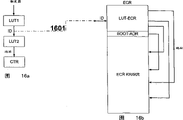
The basic structure of a CT
The summary of following relevant CT can comprehensively illustrate the situation of each structure category.Below the structural group class is described in detail.
The core of a CT is control state machine (CTs), and this controller control configuration routine (KRs) is all finished.Cooperate having of CTs, the Garbage gatherer, KR is removed in this gatherer control from the storer (CTR) of CT; FILMO, this FILMO management still needs the KWs that finishes, and the LOAD-state machine, the download of this machine control KRs.
The equipment of this storer (CTR) is as common writing-read-storer, can be used for carrying out all technical assignments simultaneously, and be used for to separately CT and place the KRs of the CTs below it to carry out part storage.(CTR) also can be equipped for ROM as the special circumstances storer, EPROM, and EEPROM, Flash-ROM or the like, fixing in order to be equipped with one to module, the function of ASIC or similar PLD (seeing the level of technology).
Use 4 indicators in order to design the CTR address as the counter equipment of downloading:
1. room indicator (FP).Be presented at the memory location of KR last among the CTR the 1st sky afterwards.
2.Garbage indicator (GP).Show a project from CTR, removing by Garbage gatherer (GC).
3. motion indicator (MP).Be presented at a memory location among the CTR, from this position one effectively, the configuration speech (KW) that should not remove, a KR project is duplicated/is moved on the project of determining by GP in other words.
4. program indicator (PP).Show instantaneous KW by CTs output.
KW continues to transfer on the relevant CELs by an output interphase.In case they are to accept KE at the state of a reconstruct, CELs replys (instruction) (ACCERT).If a KW is not replied (REJECT), in the storer of a similar FIFO, give intermediate storage so according to the time, so that in the back in the time, do not utilize program indicator, and on the CEL of selected address, write out again.
The requirement of finishing a KR comprises these CTs by flop signal.Flop signal is through a shielding, and this is a wave filter, and it filters unwanted trigger.Can get and can set up a shielding by element by UND according to technical merit, this shielding be carried out UND to a trigger with an output signal and is connected.Trigger converts binary signal to through the Round-Robin-moderator (SCRR-ARB) with preferred effect.Round-Robing-moderator with preferential interaction combines the advantage of the synchronous answer of a Round-Robing-moderator with the identification of a beat to next one output, and in other words, this is the advantage of preferential first a-moderator.
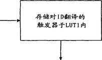
The trigger that has shielded is connected to above one the 1st Lookup table (LUT1) as the address, and this is a storer, and this storer is given the trigger that enters as the address ID coordination of relevant KR, and exports on data circuit.
In one the 2nd Lookup table (LUT2), the address of the memory location of the KR in CTR is given in the ID coordination of KR.The 2nd Lookup table not only carries out the coordination of flop signal, more is to utilize order, and these orders use an ID as parameter, and LUT2 carries out the address coordination equally.
Flop signal is that the order (REFERENCE) of setting forth below is logged among the LUT1 at the coordination of relevant Ids.The management of LUT2, Ids takes place by CTs and GC automatically at the coordination of the address among the CTR in other words.
In order to understand CT better, list a possible order sentence below:
1.BEGIN<ID>
By BEGIN<ID〉expression configuration routine beginning.<ID〉the clear and definite identifier of configuration routine is described.
2.STOP
Represent the end of a configuration routine by STOP.On this position, allocation list (CT) finishes the processing of configuration routine.Garbage-gatherer (GC) finishes the removing of the project of this configuration routine.
3.EXECUTE<ID>
Jumping is to the beginning of a configuration routine (BEGIN<ID 〉).If this configuration routine not in the storer of this CT, gives requirement by placed on it CT to it so, perhaps from storer, come out to be downloaded.
4.LOAD<ID>
Require CTE KR<ID of placed on it 〉.
5.REMOVE<ID>
Call in GC, so that fertile configuration routine<ID from beginning (BEGIN<ID 〉) to end (STOP)〉from the storer of this CT, removed, and the configuration routine of back is constantly advanced, up to not existing owing to till removing configuration routine and forming the storer hole.
6.PUSH<FORCED><ADDRESS><DATA><EXIT>
Configuration data<DATA〉write on the register<ADDRESS.If substitution<FORCED 〉, even the RECONFIG-Flag (flag) of the relevant destination register of not substitution also will write data.Use<EXIT〉and should show that this is related to a KWR, it continues output by the KWRs that REJECT interrupts the back.
7.MASK<SR><TRIGGER>
Employing<TRIGGER〉shielding of substitution trigger, or employing<TRIGGER it is resetted, depend on<SR (Set/Reset).
8.WAIT<UNMASKED><TRIGGER>
Stop the processing of configuration routine and wait for trigger<TRIGGER 〉.If substitution<UNMASKED 〉, then no matter the state of trigger-shielding records on the desirable trigger.
9.TRIGGER<TRIGGER><CT#>
The binary value of a trigger sent to place the top CT that passes through the selected address of CT#.
10.GETBUS/GETCTS
Foundation is with respect to the connection of Inter-CT-Bus.
11.LOOSEBUS/LOSECTS
Remove the connection of relative Inter-CT-Bus.
12.REFERENCE<TRIGGER><id>
Numerical value<ID〉at address<TRIGGER〉write LUT1 under the condition, give a flop signal with the KR coordination of this regulation.
These order EXECUTE, LOAD, and REMOVE, PUSH, MASK, WAIT, TRIGGER, REFERENCE is only at BEGIN ... the STOP bracket is with interior effective.Beyond this bracket, do not export these orders.
The structure of a configuration routine (KR) looks following these situations that resemble.
BEGIN<ID>:
The order that is suitable for
STOP;
Indirect addressing (quoting)
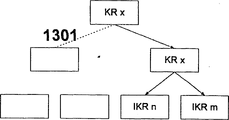
Cache memory principle among the CT can be carried out buffer-stored to KR on CT, and can use KR from a plurality of different lower level CTs or CELs.
If the external interface of the unit access module (as RAM, peripherals) of lower level then is necessary to store the different addresses or the various piece of external interface.This will make the content fundamental difference of each required KR.The possibility of no high-speed cache.
Indirect referencing provides a kind of remedial measure.Must use the special KR (to call IKR in the following text) that comprises and set necessary external parameter for this reason.Perhaps other different KRs can call in different classification aspects through trigger.Call in actual KR from the end of IKR.But, IKR can't high-speed cache, and the KR that is called in is on all four, therefore can high-speed cache.Suggestion is reduced to absolute minimum with the size of IKR, just outside and different parameters and calling in the KR of unanimity.
Indirect configuration routine (IKR) can followingly be set:
BEGIN<ID>;
…
* *; Effective order only can start peripherals,
TRIGGER<ID 〉; Start, stop or loading request to peripheral processes.
…
GOTO<ID 〉; Jump to consistent KR.
Special case:
1.WAITL?FOR?BOOT
This order is only applicable to first address of CTR.In bootup process, be written into CTR during complete Boot-KR initialization, but do not write Boot-KR BEGIN<0〉the beginning sequence.In Boot-KR BEGIN<0〉to locate (address 1) be WAIT-FOR-BOOT, can when RESET, be provided with automatically.Have only after whole Boot-KR is written to CTR, WAIT-FOR-BOOT can be with BEGIN<0〉carry out toppedly, CTS begins treatments B oot-KR.
WAIT-FOR-BOOT must not occur in a program.
2.BOOT<CT-ID>
BOOT<CT-ID〉shown which CT the Boot-KR of back should be written among.At Boot-<CT-ID〉not BEGIN afterwards, Boot-KR is not by STOP, but a BOOT<CT_ID by subsequently close.STOP finishes bootup process.
BOOT<CT-ID〉must not in a program, occur.
Bootup process
After RESET, the CT of uppermost classification face (ROOT-CT) calls in Boot-KR among the CTs of following classification face.Therefore, when arriving the address (BOOT-ADR) of a defined, occur jumping, promptly list the exterior arrangement storer (ECR) of ROOT-CT in.ROOT-CT carries out this jump, obtains boot.Can carry out following setting:
BOOT<CT-TD1>;COMMAND;COMMAND;…
BOOT<CT-TD0>;COMMAND;COMMAND;…
…
BOOT<CT-TDn>;COMMAND;COMMAND;…
STOP;
In bootup process, whole Boot-KR at first is written to from by<CT-ID〉the CTR of address 2 beginnings of the CT that lists.The start program of Boot-KR (BEGIN<O 〉) is not to be written in the address 1.On this position, be WAIT-FOR-BOOT, can when RESET, be provided with automatically.As long as after whole Boot-KR is written to CTR, and ROOT-CT arrives BOOT<CT-ID subsequently 〉, STOP just can be written on the CTR of Boot-KR end, with BEGIN<0〉modification WAIT_FOR_BOOT.CTS begins treatments B oot-KR.
Calling in of configurator
For configurator of request outside Boot-KR, three big basic mechanism must be arranged:
1. carry out LOAD<ID by CTS 〉
2. carry out EXECUTE<ID by CTS 〉, in CTS, do not contain the KR of corresponding ID.
3. transfer to one<ID through LUT1〉the appearance of trigger, the KR under in CTR, not having.
The process of these three kinds of situations is the same:
In LUT2, list the ID of requested KR as the address.This LUT2 checks whether an effective address is arranged in CTR.If do not have, that is to say<ID〉in LUT2, be shown as 0 value, then load<ID〉quilt reached CTS.
Then, when the higher level CT of classification, CTS request and<ID〉relevant KR.This request arrives higher level's CT in the mould of a trigger, and correspondingly it is calculated.
This higher level's CT is sent to requested KR the CT of the request of sending.These data are write into CTR from the shown address of FREE-POINTER (FR), and this FR is improving one behind the record accessing each time.
If FR has arrived the upper limit of CTR, then must call in gibberish collector (GC), to remove orlop KR and the compression CT R in the CTR.FR has reset like this.This process until the KR that is about to call in fully and CTR just calculate end when matching.
The skip list of config memory
The config memory that is assigned to ROOT-CT comprises all KR that must call in use.Externally in the config memory (EDR), a jump that enters the boot configuration program is arranged in the address of a defined (ADR-BOOT).And in the memory range (LUT-ECR) of another one defined, yet the length of being scheduled in use inside arbitrarily can jump to KRs separately.Any one KR<ID〉can in ECR, use as the address, and the starting address of any one KR is all at there; The KRs indirect addressing is as follows:
TD→LUT-ECR→KR
In config memory, change KR
Should change ID<A〉KR.At first, HOST is with ID<A〉in new KR write a vacant memory location among the ECR.ID<A〉will be in config memory the new address of KR, write on the predetermined ROOT-CT register from superior unit (HOST).This ROOT-CT will order REMOVE<A〉send among all CT of subordinate.Reaching STOP or when IDLE circulation (only otherwise carry out KR) then, all CTs have eliminated the KR that is related with ID among the CTR, LUT2 is set to the address<A of " NoAdy " 〉, that is to say, at ID<A of LUT2 in do not have the input of effective address.If ID<A〉regain request, enter position<A of LUT2〉that input that lacks (" NoAdy ") of locating forces each CT to ask KR<A among the ECR again 〉.
FILMO
KR mainly is made up of order PUSH, and this PUSH can write new configuration language on the specific address.If can't write the configuration language of model KW, because this element that can dispose (CEL) with address is unwilling to receive new configuration (REJECT), then this configuration language is not to be written to that to have the element that can dispose (CEL) of address but be referred to as below being written on the storer of FILMO.The order of back can obtain normal operation, till a configuration language can't write again, and this configuration language and then write among the FILMO.
If can't write the configuration language of model KWR, because this element that can dispose (CEL) with address is unwilling to receive new configuration (REJECT), be not to be written to that to have the element that can dispose (CEL) of address but be referred to as below being written on the storer of FILMO to this configuration language.The order of all back (to the KR end) is write CEL but on the FILMO that writes direct with blocking.
FILMO will be moved fully at the IDLE circulation time with before the each execution of a new KR.Therefore, when starting the oldest data word and consistent with the FIFOs of state of the art, the FILMO language that any one is read out must be sent on the element with address; Thereby this element with address must be willing to receive this configuration language.As long as these data words can write (that is to say that those elements that can dispose (CEL) with address are got ready) from the beginning, then must remove input among the FILMO according to the mode of a FIFOs.If can't write configuration language, must skip it so, from FILMO, do not remove.Opposite with FILMO is that these data can continue to read after the configuration language of skipping.The configuration language that can write after a configuration language of skipping can be according to the automatic coding of FILMO or 1.: write mark under the fashionable work, from FILMO, do not remove, the configuration language of writing mark under the fashionable work like this can not be read out when operation subsequently, but be eliminated the words that the configuration language that a short of quilt is skipped occurs previously at them at once; Perhaps 2.: remove from FILMO, these configuration languages are before the configuration language that is eliminated and all exist afterwards like this, thereby in order to obtain removing, the language of back must be moved to front (top) or the language of front must be moved to back (following), in any case therefore must keep the order of configuration language.
If carry out new KR, then those configuration languages (KW) that can't write the element (CELs) with address from CTS will track to FILMO again, that is to say, KW will write the end (tape reading direction) of FILMO.If FILMO is full, promptly there is not the vacant input of configuration language, then the execution of KR will stop.FILMO waits until when having write enough configuration languages and many vacant inputs correspondingly having occurred always and just finishes operation, and KR will continue the execution computing.FILMO provide one with the similar storer of FIFO, can begin linear running from the oldest input all the time, and different with FIFO be to skip input (at first in linear multichannel outlet).
The function of allocation list Statemachine (CTS)
CTS exercises the control to CT.It carries out the order of KR, and is reacted on the trigger, and it exercises the management to FILMO, can read FILMO in the IDLE circulation and before execution KR.It is reacted to the signal illegal<TRG that is produced by the LUT structure〉(illegal trigger can be referring to Fig. 1,0102) and load<ID 〉.When occurring cache memory failure (0105) on the LUT2 or passing through KR/IKR that ID inquires about eliminating mark (0107), just can produce load<ID 〉.It is reacted on the control signal of higher level CT.
The automatic coding of processing command sees also Fig. 2-7 for example.
The higher level CT of control signal
-illegal<TRG>(0102)
Represent to higher level CT, a not clear toucher<TRG occurred 〉.
-load<ID>(0105/0107)
Inquiry higher level CT is to call in<ID 〉.
-trigger<TRG>(CT#)(0108)
Send a toucher (TRG) to the higher level's or have a CT<CT# of address.
The control signal of higher level CTs
-remove<ID〉(referring to Figure 15,1513)
Inquiry CT is with removing<ID 〉
-write_to_FP<data〉(referring to Fig. 2,0205)
Send data to CT.Data tracking is to the end of occupied storer.
The function of gibberish collector (GC)
CTR is subjected to the restriction of two problems:
1. give directions LOAD or EXECUTE command and trigger to note ID, the KR among the ID does not have in CTR, must be called in after a while voluntarily by KR.Yet there are not enough spaces when sometimes in CTR, calling in requested KR again.
2. REMOVE<ID appears〉time must from CTR, remove corresponding KR.Like this, only otherwise be positioned at the end of CTR, an interval will appear.When calling in new KR, sometimes this can not be filled at interval again fully, and perhaps this is too little to new KR at interval.This will cause the part figure of a CTR.The task of gibberish collector just is, from CTR, remove KR, so that all remaining KR must be connected on the storer as the closed routine piece for new input space for the creativity and when removing input back reorganization CTR, those vacant storage blocks be placed in the end of CTR as a closed routine piece.
Like this, new KR just can be at best mode and is replenished with having no loss and call on the memory location.
The utilization of trigger pip
Each CT all can be connected on a plurality of flop signal that belong to its classification face separately, and these flop signal reassociate on the bus.These detailed triggers will obtain utilizing in a shielding, that is to say, the flop signal that only can relay transmission freely connects.These flop signal that freely connect with beat synchronously intermediate storage in a sampling register.The operator can select one of them stored flop signal, and this signal is changed into a binary vector.Selecteed flop signal can obtain removing from the sampling register.But this binary vector relay transmission is to first search graph 1 (LUTl), and this LUT1 converts binary vector to the identification number (ID) of the configurator (KR) that obtains asking again.This ID converts the KR address in the CT storer (CTR) again in second search graph (LUT2).CTS (CT-Statemachine) is set to its program indicator (PP) on this address, and begins to carry out KR.Precondition is that any one trigger that freely connects in shielding all has a corresponding input outside LUT.If no, this error condition goes up (illegal trigger) with relay transmission to CTS so, and each ID that therefore is equal to " NoAdr " can be calculated as the input of non-existence." NoAdr " is a selectable sign that depends on automatic coding.
If on LUT2, lack input, that is to say that the KR relevant with ID be not on CTR, the request of calling in must be sent to CTS and go up (load<ID 〉) so.
Trigger pip sends to higher level CT
The interface of utmost point CT also exists the another one interface to call in outside the KR in the arrival that had illustrated, can exchange the order that freely defines especially trigger vector.Therefore CT or send order (BROADCAST) to all other CTs perhaps has CT transmission order (ADDRESSED) of address to any one.
This order " trigger vector " (Triggervector) provides a binary value, inquires about in the time of can be imported in receiving the LUT2 of CT.
It is necessary sending the trigger vector, as starting KR an IKR inside in another one CT, as regulating peripherals or storer.
For relay transmission trigger vector to a higher level CT, must there be two mechanism:
1. this LUT1 must replenish a bit, and the content that storer is described is considered KRID or is considered the binary value of trigger pip.If a trigger pip is arranged, then the data content of LUT1 can directly be sent to utmost point CT as trigger.
2. the binary value of a trigger just can illustrate that with order TRIGGER it can directly be sent to higher level CT.(also can directly transmit ID rather than trigger value selectively).
When starting KR among the outside CT on the trigger vector, must implement method for synchronous for obtaining no deadlock.The method must be noted that it only is other KR of starting on a KR other CTs in this group in the specific group of CTs.The starting of a plurality of KR can cause the deadlock between the CTs simultaneously, and is similar with the deadlock of having described on the CEL grade.
The cardinal rule of said method is as follows:
The structure of a KR is as follows:
GETCTS/GETBUS
TRIGGER<ID>,<CT#>
TRIGGER<ID>,<CT#>
LOOSECTS/LOOSEBUS
The order " GETCTS " of the KR inside among the CT (INITIATOR) shows that following signal will send among other CTs (TARGET).With Trigger<ID 〉,<CT# 〉, the ID of a KR who starts will send on the CT in company with unique IDCT#.Direct higher level CT is at first arrived in the transmission of trigger, and it is consistent with CT# to be sent to a new CT of subordinate in the CT scope with trigger or to be sent to the higher level CT (can referring to the CT classification) its there.If this order has arrived TARGET, then TARGET can reply reception.
When the order by a CT moved, the preferential identification of this order was always risen one.When another one request in the CT was run in the relay transmission request of an order as a result, this order will be refused first degree preferential.Therefore must guarantee a) that the same time is only transmitted one thereby also can only start a KR in an afoul system, and a KR can cause needed no deadlock.
B) must guarantee that refusal is up to now at least still in the order of propagating, and this order can cause the raising of performance.
After order of refusal, all above-mentioned orders in GETCTS/LOOSECTS inside are all refused equally, that is to say that INITIATOR sends signal DISMISS to all TARGET, will after one period waiting time, when GETCTS, start again and carry out KR.
At an instruction section GETCTS ... replying of all triggers in the LOOSECTS will be sent to INITIATOR-CT.Be about to arrive each time reply the time, will proceed the processing of next instruction.
When obtaining instruction LOOSECTS, INITIATOR has sent signal GO to all TARGET.Therefore TARGET-CTs starts execution KR with the ID by the trigger transmission.
A kind of situation below TARGETs is varied to after trigger of appearance, promptly this moment, they were in the appearance of waiting for GO or DISMISS signal.
Because better automatic coding can be seen a kind of method that is easy to revise in addition: between the CTs of a group of classification aspect, a bus system (Intex-CT-Bus) is arranged.This bus system has connected CTs and CT who directly belongs to this group of all these groups.
By this instruction GETBNS (similar with functional GETCTS), this bus system will be judged by a CT.These instructions will be through this bus system by the CTs of relay transmission to same group.If in this group, do not have the CT# of address, then can judge its higher level's bus voluntarily by this higher level CT, this instruction will obtain relay transmission.Therefore these buses of being judged will still be distributed INITIATOR and be forbidden all other CTs, until otherwise refuse, or till the instruction LOOSEBUS decomposition bus.LOOSEBUS can compare with LOOSECTS.Before execution command LOOSEBUS, the GO signal is sent to the CTs of all participations.This can carry out by instruction LOOSEBUS or by the instruction of a distinctive pre-starting.Instruction and trigger will be handled according to the basic skills of describing already equally.When can't obtaining judging, a bus system just can refuse.When judging, the CTs of a grade always obtains preferential at once, and higher level CT has higher preferential.When sending an instruction on Intet-CT-Bus, this instruction must keep active state always, till the CT with address accepts this instruction (ACCEPT) or refusal (REJECT).
Preferential Round-Robin-moderator
The structure that preferential Round-Robin-moderator (single cycle-Round-Robin-moderator SCRR-ARB) has clock synchronization, promptly each-according to implementation status positive or negative-clock period at interval (TFI) moderator one result all is provided.Entering signal (ARB-IN) transmits by a shielding (ARB-MASK), and this shielding is managed according to following process automatically by moderator itself.The output signal of shielding is according to the relevant technology priority moderator (ARB-PRIO) that offers, each all period interval (TFI) moderator and system clock are synchronously exported a result (ARB-OUT), that is: the dyadic number value of the information of the limit priority after shielding (ARB-MASK).A signal (VALID) is assigned to this result, and whether this dyadic number value of this signal indication is effective.Can be when signal 0 is arranged and produce same dyadic number value when the no signal according to the performance of priority arbitration device: VALID represents in this case: the result be invalid if no signal exists.This signal is:
1. the result as moderator is output.
2. deliver to a demoder, this demoder is decoded as for example dyadic number value shown in the following table to a 3-position dyadic number value.(this cataloged procedure is suitable for any required dyadic number value according to this principle).
| The dyadic number value | Decoding | Note |
| (ARB-OUT) | (ARB-DEC) | |
| 111 | 01111111 00111111 00011111 00001111 00000111 00000011 00000001 11111111 | |
| 110 | ||
| 101 | ||
| 100 | ||
| 011 | ||
| 010 | ||
| 001 | ||
| 000 | Reset mode and when dyadic number value (ARB-OUT) is invalid |
A register (ARB-REG) is affixed to demoder, the numerical value (ARB-DEC) of this register decoding of Rcv decoder when the clock pulse (TF2) of asking in reply in TF1.ARB-DEC is fed back to shielding and goes up (ARB-MASK) and discharge single input signal (ARB-IN).
Mechanism in processor is as follows:
1. all ARB-NI (input signal) are released by ARB-MASK (shielding) after the RESET that once resets, because ARB-DEC (demoder) is transferred to all signals in " release ".
2. be set to prepreerence ARB-IN (for example in the above table signal 7 (binary one 11) have override power and signal 0 (two advance 000) least preferential) be used as the dyadic number value and export.
3. process ARB-DEC signal is by locking, in case all other inputs more preferentially but are not set up.
4. the 5th and 6 following steps repeat always, arrived up to signal O (two advance 000), or till the ARB-MASK back does not have signal.Then ARB-DEC (referring to decoding table) discharge all by ARB-MASK through the signal of ARB-DEC and flow process in the place's beginning of the 2nd step.
5. the ARB-IN of override setting this moment is used as the dyadic number value and exports.
6. in case all other output more preferentially but is not set up, signal through ARB-DEC just by locking.(continuing for the 4th step).
So just can handle comparably all input signals and each beat circulation time of one in input signal (ARB-IN) all input signals be interpreted as two advance value and output (ARB-OUT).ARB-REG can join one and activate an input (EN), and it only just allows the modification of content of registers when TF2, if there is corresponding signal to exist.Thus, one two is advanced vector and no longer is output when each beat, but with relevant with the release that TF2 produces by EN.When the conversion of back can not be carried out processing in a beat circulation, and need a plurality of circulations and just accept next two then when advancing vector, input is for necessity synchronously.
At the great majority of signal when All factors being equal, preference will be give to, perhaps to be considered to by processor comparatively preferentially be significant to a series of signal.This for example describes in front when being used for continuing transmitting the method for signal between CT is necessary.In order to make a signal more preferential, the prepreerence connection of ARB-PRIO is not covered, that is: transmitted from shielding (ARB-MASK) is other.Signal is by priority processing thus.
The structure of CT on the basis of microcontroller
With description difference so far, a CT also can be performed in a microcontroller architecture.
Be readily appreciated that: those basic functions, as trigger control, check table LUT1 and LUT2, and between CT communication and KW is write CEL all directly can be complete by a microcontroller.Just the structure of the FILMO that efficient is high has and at first can reach the problem that is just found out in the performance.Therefore, the structure of FILMO has been studied especially.
The structure of FILMO
FILMO is not used as independent storer.This common program storage has been expanded the FILMO-function more.Therefore an additional position (FILMO-position) is assigned to each KW, and it shows whether corresponding KW has been written into CEL.If the FILMO-position is set up, so corresponding KW just is not performed.The FILMO-position is reset a KW write store time.All KR in CT interconnect in order through a chained list (FILMO-table), as them be triggered device or LOAD<ID〉call in.KR in the FILMO-table, is performed up to it always fully, and it is removed from table then.The FILMO-table also becomes a direct substitute of FILMO-storer thus according to the operation of FILMI-method.
(for integrity, as can be seen with original FILOM-method on the contrary in table a KR can not occur once more.If one also the KR in FILMO-table be called, its execution must be delayed so, until it by from the removal of FILMO-table.)
The structure of a FILMO-memory location is as follows:
| The FILOM-position | KW |
Order
Microcontroller supports the following order that FILMO is had a direct impact: PUSH that a KW is write CEL PUSHSF a KW to be write CEL and FILMO-position PUSHRET is set when KW is accepted (ACCEPT) KW is write CEL and return (RETURN) from subroutine, when KW not by CEL
When accepting (REJECT).This order is used, when the KW that follows in KR gets
When determining configuration in this KW (ACCEPT); Its configuration is by returning from KR and hinder,
Till PUSHRET success (ACCEPT).PUSHNR writes CEL to a KW, has only when REJECT not occurring in KR inside in front.
Effect is similar with PUSHRET, is used for using in the dependence of configuration sequence to KW.
Dustbin
So far explanation is consistent together, and a dustbin (GC) is used to delete the KR that no longer needs.When in storer, not having new KR of enough space loadings and ID necessary deleted; Perhaps when a KR shows that by order REMOVE-the ID-of the KR that will delete is deleted significantly, the GC startup.
In order to make the GC-process simple as far as possible, all KR connect each other by the inventory of a link.GC scans an inventory and deletes the KR that those no longer need, and is logined correspondingly adaptive deletion of quilt by these KR by other KR covering and inventory.This moment, all KR that stay in storer correspondingly moved, and made owing to deleted that storer room that KR produces is filled up and at last generation bigger continuous free space of storer.
The structure of a KR
In tabulating down, listed the presumable essential structure of a KR:
| ????jmp?START |
| ????Iength |
| ????garbage-previous |
| ????garbage-next |
| ????FILMO-previous |
| ????FILMO-NEXT |
| ????CACHE-statistic |
| ????KR-statistic |
| ????START |
| ????ret |
Jump of generation comes the startup command sequence through the controller of back when KR begins.And then be the inventory that is used for dustbin of double link, KR all in this inventory interconnect.
" length " illustrated the length of KR.This information can be used for Block-Move-order (program block-move-order) according to the technological vision situation, and these orders (rubbish loads etc.) when KR is must be in storer mobile are employed.FILMO forms in the inventory of back to back double linkage, and only contain those KR that are not written into the KW of CEL as yet this moment is interconnective.Produce the statistics about speed buffering-state, what it comprised KR for example calls in number of times (whenever call in a numerical value and be enhanced 1), timeliness (quantity according to the GC-process by KR can record) etc.This statistics can must be through by when deletion statistical study GC from storage space at a KR.For speed buffering, produced very big advantage by these statistics.Can adapt to microcontroller programming, consequently with the requirement of using for example according to employed speed buffering-algorithm like this
1. the oldest/up-to-date KR
2. minimum/maximum KR (referring to login " length ")
3. minimum/the most frequent KR that calls in is deleted from speed buffering, when the storer of needs sky.This moment, conspicuous other useful status information can be stored, and this kind optionally is buffered in existing known speed buffering-structure can not.Particularly the cache algorithm of freely programmable is not supported according to existing technology in speed buffering.
KR one statistics is arranged at last, and it comprises (REJECT) that for example is not configured or the quantity of (ACCEPT) KW of being configured.The address of first KW that also need must dispose can be stored simultaneously.Its advantage is: can leap in a FILMO-process above the KW and needn't pass through KR, so just improve performance greatly.
At last for KR be noted that the inventory that is linked preferentially previous by logining/back one-ID is formed, because absolute thus storage address can be moved without a doubt by GC.In a KR, should only use and jump relatively rather than absolute the jump, avoid when loading KR and in the GC-operational process, have problems, because this moment, specific address can change.
For integrity, must propose be according to the principle that has illustrated when using microcontroller before carrying out a new KR (based on a trigger or an order, also from another CT) FILMO also will through and in that (convertible configuration or can not alternate arrangement) will be guaranteed through the state of CEL before the FILMO.
Figure
The figure that describes below carries out the management that example has illustrated the configuration data that carries out according to the method for being introduced by means of one:
Fig. 1: the method that in tracing table, produces the address
Fig. 2-7: the function of processing command and state instrument
The structure of Fig. 8: SCRR-ARB
Fig. 9: LUT1﹠amp; The structure of LUT2
Figure 10: the structure of pointer arithmetic sum CTR
The structure of Figure 11: FILMO
The grade configuration of Figure 12 a:CT
Figure 12 b: the transmission of the trigger between CT
Figure 12 c, d: the sending method of trigger vector
Figure 13: call in a KR by a plurality of IKR
Figure 14: the structure of the LUT1 of a ROOT-CT
Figure 15: the HOST-control structure of a ROOT-CT
Figure 16: LUT and ECR notion are described
Figure 17: the process control of the CT of intermediate grade layer and a ROOT-CT
Figure 18: the deadlock when the configuration of the array of a 2-dimension is buckled problem (referring to patent description)
Figure 19: the FILMO-notion is described
Figure 20: the ultimate principle of communicating by letter between CT
Figure 21: the execution of communicating by letter between the CT according to the GETCTS-method for example
Figure 22: the execution of communicating by letter between the CT according to the GETBUS-method for example
Figure 23: the bus-bar construction of bus between CT
Figure 24: the address in the CT-grade
Figure 25: rubbish-inventory
Figure 26: FILMO-inventory
Figure 27: the FILMO function in KR
Figure 28: store status before carrying out a KR or FILMO
The explanation of figure:
Fig. 1 has shown the process that the CTR-address in a CT produces.Be translated an effective KR or IKR ID at one in the LUT1 two detailed trigger vectors (0101) that advance this moment.If there is not effective I D to exist, so just produce a signal " illegal trigger " (0102), this information explanation trigger is not identified in LUT1.This problem can be used as error message and is gone up or be left in the basket to upper level CT by relay transmission.Translation from " trigger " to " ID " is logged on the LUT1 by means of " REFERENCE " (reference) order.An effective I D (0103) by relay transmission to LUT2.Inner ID (0104) by an operand explanation directly arrives on the LUT2 in order.In the address of the KR/IKR that LUT2 translates a detailed ID in CTR inside.If KR/IKR is not stored in (not in speed buffering) in the CTR, information " Miss " (lacking) will be produced (0105) so.If the address that is translated of KR/IKR indicates signal " NoAdr ", use " No Entry " (0107) presentation address deleted so." Miss " and " No Entry " expression cannot be translated on the address of CTR-inside.On the basis of this signal, loading-state machine refills with the ID of a corresponding CT placed on it and carries a KR/IKR.
As long as there is an effective address, this address just is sent on the pointer algorithm of address generator (0106) so.One detailed two is advanced the trigger vector and is translated into an ID or another trigger vector in LUT1, and this moment, the trigger vector was output (0108) in this case.
In Fig. 2, the process when loading a KR/IKR is illustrated.At first, the ID of the KR/IKR that be loaded (0201) is sent on the CT placed on it.Then, the numerical value at the login place free pointer (FP) of desired ID is registered among the LUT2.FP sensing last in CTR is used for the registration of the registration back of a KR/IKR, and this is first registration of having stored the KR/IKR that will load thereon.
State machine is waited for the data words and expressions of CT placed on it.In case words and expressions can be used, it just is written on the position of being pointed out by FP.FP is by increment, if the login behind the end of FP sensing CTR, the login of first in CTR is removed so, in order to space for the creativity (0202); This moment, FP was implemented.If the data words and expressions that is sent by thereon CT be " STOP ", loading process is stopped (0203) so, otherwise, continue new data words and expressions (0204) of wait.
In Fig. 3 a, represented " MASK "-order.The operand of order is written in the MASK-register.Before the input of the flop signal of MASK-register-bit before LUT1 and mark invalid trigger.
In Fig. 3 b, the operand of order is used as the trigger vector by order " FRIGGER " and sends on other CT.
In Fig. 3 c, translate quilt for the trigger of corresponding KR/IKR ID and write LUT1 by order " REFERENCE ".
Expression order " WAIT " in Fig. 4 a.The operational data of order writes the WAITMASK-register.All triggers, up to waited for and in WAITMASK, discharge thus, all be left in the basket.Only behind trigger, just turn back to program flow.In Fig. 4 b, " PUSH "-order is described.The configuration words and expressions is sent to the configurable element (CEL) of addressing and locates.If CEL does not accept to dispose words and expressions,, dispose words and expressions so and be written into (0401) among the FILMO because for example CEL is under " non-configuration " state.
Fig. 5 points out the process of " REMOVE "-order.Have 2 to call in variable:
1. the 1st KR/IKR in CTR deleted from CTR, and the address of CTR is assigned to rubbish pointer (GP) (0501).
2. the KR/IKR by its ID explanation of a special use is deleted from CTR.The 1st address of the KR/IKR that will delete in CTR is assigned to rubbish pointer (GP) (0502).
Moving hand has been loaded the numerical value of GP.Even if first KR/IKR should be deleted from CTR, GP and MP also will point among the CTR one " BEGIN<ID〉" order.It is invalid to be denoted as among the LUT2 of relevant ID.MP is by increment, and " BEGIN<ID〉" at the KR/IKR of storer is reached up to the next one, and ODERMP equals free pointer (FP), and this KR/IKR that indicates to delete is last (0504) among the CTR.
In this case, FP loads onto the numerical value of GP, and the memory location that is occupied by the KR/IKR that will delete is denoted as empty like this; Function " REMOVE " finishes (0505).
Otherwise (" BEGIN<ID〉" is reached (0506)), the data of being pointed out by MP are copied on the memory location of being pointed out by GP.MP and GP are by increment.This process is performed until (0507) till the position that MP arrives CTR end or FP.If one has the memory location of " BEGIN<ID〉" to be pointed out by MP therein during the course, just the login that is used for corresponding ID in LUT2 is rewritten (0508) by MP so, correct memory location is output when checking thus.
Fig. 6 points out the procedure chart of FILMO.A FILMO contains 3 pointers:
1.Write the write pointer of P:FIUMO-RAM
2.Write the read pointer of P:FILMO-RAM
3.Write P: represent " occupied state " of FILMO-RAM and prevent too much and not enough case pointer.
One one register " BeginF " shows that whether actual read access is positioned at the beginning (TRUE) of FILMO-RAM, does not have not deleted login between the beginning of read pointer and FILMO-RAM that is:; Or read pointer is positioned at the central authorities (FALSE) of FILMO-RAM, and promptly useful login is between the beginning of read pointer and FILMO-RAM.In addition, also have two register at the state that is used to store ReadP and FullP.When first not deleted login occurring, must protect two registers, because when a read access that carries out later, must begin to read on the position in this login.On the other hand, ReadP and FullP but must continue to be modified in actual read procedure, obtain the following terminal of reading address and definite FILMO-RAM.So because the similar of FILMO is in FIFO-structure-all can not be determined by means of an address 0 or a maximum address as the beginning and the end of so-called circle storer-storer.From basic status, draw two operating paths:
1. read path (0601)
FullP and Read P are secured at register.Treatment loop begins:
BeginF is TRUE.
If FullP equals 0, Read P and FullP are read back from its register (0602) and state machine returns basic status so.
The login pointed to of (0603) tested whether RaedP in FILMO equals " NOP " in addition, relates to a login that is designated as deletion in FILMO central authorities that is:.(0604) if not so will write (CEL) in the configurable element to login so.As not all right words (REJECT, 0605), because CEL is immutable configuration, BeginF is set to FALSE so, FullP decrement and RaedP increment.State machine jumps to the place that begins of treatment loop (0606).
If login is write CEL success (0607), or log on as NOP, BeginF is tested so: BeginF=TRUE (0608): do not have not deleted login before it.FullP is by increment, and ReadP is guaranteed to keep the NEW BEGINNING of FILMO in the register of distributing to.FullP is guaranteed to be used to keep the data volume of reality; ReadP is by increment.
BeginF=FALSE (0609): FullP is rewritten with NOP by increment and the actual log in FILMO-RAM; That is: login is deleted, and ReadP is by increment.
State machine all jumps to the place that begins of treatment loop in both cases.
2. write path (0610)
Whether test FILMO-RAM by the FullP on the check greatest measure full.
If full (0611) is then jumped to and is read to obtain in the path space.
Otherwise the data words and expressions is written among the FILMO-RAM and WriteP and FullP increment.
Fig. 7 is presented at the process in the host state machine.Basic status (IDLE) is left, in case
1. the REMOVE-Kommando (moving an order) (0701) that a position CT thereon occurs; Movement directive is performed, and state machine returns IDLE.
2. a trigger pip (0702) that is used to produce trigger appears between CT; Trigger is output.
State machine is jumped into " STOP " order, then returns IDLE.
3. occur one and be used to carry out KR/IKR<ID flop signal (0703): program pointer (PP) is loaded by the address that is produced by LUT2.If the address is invalid, that is: be used for the login of the KR/IKR that will load in existence, then KR/IKR is loaded (0704) and PP resets.
The execution loop begins:
PP is by increment (BEGIN<ID when the operation of loop first〉order just skipped thus), the appearance that is under an embargo of other trigger, and RECONFIG is by locking.Order is performed and jumps to the beginning (0707) of carrying out the loop.
Order " STOP " is by special carry out (0705).Trigger and RECONFIG are discharged again and state machine jumps to IDLE.
Order " EXECUTE " is also by special carry out (0706).At EXECUTE<ID〉in the ID that provides be written into ID-REG.PP is reloaded and is performed (0708) by the KR/IKR that ID provides.
Basic configuration is loaded in the execution of also directly jumping into basic configuration among the CTR (0709) after CT resets.
Fig. 8 shows the structure of a SCRR-ARB.Table known to the signal process DataIn arrival shielding (0801) of judging, its basis connects the be associated part and the locking of signal.According to common priority processing device (0802) of prior art by the quantity of the signal that connects judge a signal and its two advance vector (Bi-naryOut) same effectively/invalid-sign (ValidOut) together (also according to prior art) be provided as the output of SCRR-ARB.
Table known to this signal basis is translated coding (0803) and is delivered to the register (0804) that is used for synchronous beat.Shielding is opened through this register DataIn.This moment register or by a beat or by next signal (Euable EN) control of a next effectively scale-of-two vector of inquiry.When resetting, maybe show that when invalid, register is switched on when sign (ValidOut), so that the DataIn shielding connects all signals.
Being configured in 0805 of shielding is illustrated, and shields to be illustrated again in 0806, and this moment, signal DataIn O..DataIn1 was that All factors being equal, preference will be give to according to the SCRR-principle, and DataIn m ... DataIn n is comparatively preferential.
The LUT-structure is described in Fig. 9.The scale-of-two vector (BinaryIn) of the trigger of judging is transferred in the address input of LUT1 (0901).LUT1 is this scale-of-two vector or translate in the effective trigger its relay transmission to another CT, perhaps translate in the effective I D, two all be output through 0910.0911 demonstrates that to relate to a trigger still be an ID.If do not have the two detailed translations of advancing vector to be logged among the LUT1 through order " REFERNCE ", so-by means of the login of position or comparer (for example " VOID ")-produce signal " illegal trigger " 0914 in some way.Triggering is along being directed on the outside CT through 0912, and ID is continued processing through multiplier (0902).0902 or the data output of connecting the LUT1 of an effective ID of explanation, perhaps connect the ID-register (0903) of CT and go up (0904) to the address input of LUT2.0904 has a speed buffering-similar structure, that is: the low value part (0906) of 0902 numerical value output is received in 0904 the address input, and the part of high value (0907) is pulled to 0904 data and imports.Belong to the output of 0907 data with 0907 relatively through a comparer (0905).The advantage of this method is 0904 needn't show the degree of depth that is used to translate all ID, but can analyze the littler degree of depth.Be similar to common speed buffering, have only the part of ID to be translated, in LUT2, can determine by means of 0907 whether selected ID meets the ID by the LUT1 explanation simultaneously.According to prior art, this meets the Cache/TAG-method.
-a scale-of-two vector (comparison diagram 8) appears by " ValidIn ".
-relate to a trigger when illustrating in translating LUT1 still to relate to an ID (0911, " Trigger/ID Out ").Trigger is sent on other CT through 0912.ID is processed and continue to be sent on the LUT2 in own CT.
-0905 result, it illustrates whether corresponding ID is stored in (" Hit/Miss Out ") in 0904.
-0909 result, it illustrates whether corresponding ID points to the effective address (" NoEntry Out ") among the CTR.
Continued to be sent to CTR by 0904 address that produces and gone up (" CTR Address Out ").
LUT1 is used the translation of detailed scale-of-two vector to be loaded on a trigger or the ID through order " REFERENCE ".This of order counts and is transmitted on the LUT1 through bus 0913.ID-register (0909) is loaded through identical line mother.
Figure 10 shows the pointer algorithm of rubbish pointer (PG), program pointer (PP), moving hand (MP) and free pointer (FP).Each pointer by one can separately control loading on/down-counter forms.As long as each counter can-be necessary-load with other the numerical value of counter; With output the same (1007) with LUT2.
Determine whether by comparer
1.PP equal MP
2.MP equal FP
3.FP equal the maximum position in CTR
These results are used to control state machine.
An input, address that is transmitted to CTR through multiplier (1001) in the pointer.Data through multiplier (1002) or from CT placed on it (1005) or in the register (1003) arrive on the CTR.Being continued to be sent to state machine and FILMO (1006) through the data of the data of the CT of a multiplier (1004) or upper level or CTR locates.This moment, order directly was sent on the state machine through 1004 by higher level CT when a REMOVE-order occurring, and if not, order is passed on the state machine from CTR.Register 1003 is used for demanded storage and feeds back to the CTR input, and these orders are moved to another address from an address when dustbin moves.
The structure of a FILMO is illustrated in Figure 11.Data are from CTR (1101) arrival FILMO and or process multiplier (1102) is written into FILMO-RAM (1103) or process multiplier (1104) is sent on the configurable element (1116).If data are deleted in 1103, " NOP "-signal is just write toward 1103 through 1102 so." NOP "-signal is identified and prevents to write configurable element through the comparer (1105) of data output.Through multiplier 1106, not that write pointer WriteP (1107) is exactly that read pointer (1108) is led in 1103 address input.In register 1109, read pointer is guaranteed, so that can reset (referring to Fig. 6).
1103 occupied state counter full (1110) is stored in the register 1111 according to Fig. 6 to be used to reset.Two comparer tests 1103 are empty (1112) or full (1113).The control signal of state machine (1101) selected by process multiplier 1115 or the control signal of FILMO is sent on 1116.
Figure 12 a points out the hierarchical organization of CT.All CT (1201) and be subordinated among its ECT (1204) and obtain data from ROOT-CT.All there are one or several CT for each the execution aspect in an assembly.Each CT is in charge of the CT of its aspect and lower floor.All equally dark there is no need of all branches of tree.For example, the aspect that is used to control the peripherals (1202) of an assembly is lacked than the aspect that is used for Control work element (1203).Data transfer such as tree-shaped carrying out.Each CT moves as being used to place the speed buffering of the CT under it.
Figure 12 b is presented at the trigger stream between the CT.When data stream by tree-shaped when mobile, trigger stream is not fixed.Each CT can send the CT of a trigger to other.Generally speaking, the trigger exchange is only carried out towards the direction (1201) of ROOT-CT by page or leaf (1203).Also can move in the opposite direction and transmit sometimes.
A trigger vector B roadcast (broadcasting) is illustrated in Figure 12 C, and 1205 to trigger vector of all CT transmissions simultaneously.
Figure 12 d shows a higher trigger vector, and it is sent on the CT placed on it by 1206.(ADDRESSED)-trigger vector of 1208 direct addressings is transferred on the specific CT, and this CT does not directly link to each other with 1207.
Two common KRx of IKRn and m request independently in Figure 13 in CT high speed buffering placed on it.This show this KR by whole branch buffering and also in a contiguous branch (1301) can use a common CT.
Figure 14 shows a LUT-system of revising with respect to Fig. 9, and this system is used by means of the grade aspect in ROOT-CT and CT.It is with fundamental difference of described CT so far: must come management ID-and/or trigger vector by CT, rather than single flop signal.Hand signal this moment (RDY) is assigned to each vector to show the validity of vector, and this demonstration is transferred to a processor (1401).Through multiplier (1402,1403), not that (1404) in the trigger vector are exactly that one of ID-vector (1405) is selected.The trigger vector directly arrives the address output of LUT1 and goes up (1406), these vectors otherwise just press Fig. 9 by wiring, and ID-register (1407) is also pressed Fig. 9 wiring.Opposite with Fig. 9, multiplier 1408 has three input ports (comparing 0902).Simultaneous processing is also controlled by processor 1404 in addition except by the state machine control.The ID-vector through other input port by directly through 1403 relay transmission to LUT2.Bus 1409 promptly is used for this.(also can directly be transformed on the LUT2 according to Fig. 9 ID in principle, according to multiplier (1408) at the CT place.ID can directly send to LUT2 by CEL under untranslated situation then)." Trigger/ID Out " pressed Fig. 9 and produced.One is not existed to " Valid In " signal on " Valid Out " by relay transmission according to Fig. 9.The substitute is according to judging that producing one " ValidTrigger Out " by 1401 is used for the trigger vector and one " Valid ID Out " is used for the ID-vector, how the specified states machine is not handled.Bus 1409 by through 1410 introduce one only be present in the ROOT-CT in another unit illustrated in fig. 15.
A ROOT-CT also needs an interface of leading to exterior arrangement storer (ECR) except that common CT-function, and necessary address generator and be used for the unit of managing access to the ECR.
Common CT in LUT1 ID being translated on the memory location among the CTR (referring to Figure 16 a) on detailed trigger vector translation to an ID and in LUT2.ROOT-CT translates an ID in ECR inside on the address in the ECR when access is to ECR, and the KR/IKR that is pointed out by ID on this address begins.The memory range of its sizableness possible quantity on ID is determined (if an ID for example is the 10-bit wide, get 210=1024 possible ID, that is to say and reserve 1024 logins in ECR) in ECR for this reason.Following for example in this memory range place, end, lower end and LUT-ERC of being positioned at ECR listed in order to emphasize similarity with LUT2.Translate a trigger ID on (1601) according to the CT that has known in LUT1 this moment.In order to understand better, Figure 16 b has illustrated the access on the ECR.
An ID arrives multiplier 1501 through 1410 on Figure 14 in Figure 15.ID is written in the counter 1502 that can load through 1501.1502 delivery outlet imports on the address bus (1504) of ECR through multiplier 1503.The translation of ID arrives a storage address through the multiplier/divider (1506) on 1501 through data bus 1505, and this multiplier installs to storage address on 1502.Then, CTR is read and write to the data words and expressions of corresponding KR/IKR through main frame LOAD-ECR (referring to Figure 17) from ECR, and the each read procedure of 1502 bases is enhanced simultaneously, is read up to order " STOP ".
Through interface 1507, higher level's HOST writes ECR through 1503/1506 KR/IKR.Be judged HOST or ROOT-CT through state machine (CT) this moment access to the ECT.
After assembly resetted, a basic configuration (BOOT-KR) must be loaded.Introduce the memory address of first memory location of a fixing sensing BOOT-KR for this reason.As BOOT-ADR, memory location Oh is recommended.As long as ID began at 1 o'clock, otherwise other memory location of 2ID or any one is used, and 2ID is used in carrying out example.
ROOT-CT searches in order to load BOOT-KR on the BOOT-ADR position, in case a BOOT-KR is loaded.ROOT-CT writes data toward 1502, in order to load BOOT-KR therefrom up to one " STOP " order occurring.
One of ROOT-CT inside monitoring unit receive HOST with assembly synchronously.This following carrying out:
The little 2ID in address is by 1508 monitoring, that is: by the HOST access to these addresses the time signal (ACC-ID) be sent on the state machine (CT).Similarly, BOOT-ADR is sent on the state machine (CT) through 1509 monitoring and a signal ACC-BOOT.The following reaction of state machine (CT):
If-HOST writes BOOT-ADR, this just causes the loading of BOOT-KR.
If-HOST writes BOOT-ADR to data words and expressions 0 (1512), so just determined and caused stopping of assembly through comparer 1510.
If-HOST writes the less 2ID in address, the address is loaded onto on the REMOVE-register (1511) so.Because the address meets ID (referring to ECR-LUT), the ID of the KR/IKR that is modified is in 1511.Order REMOVE<ID〉be sent to and be used for carrying out immediately (1513) on all CT.Then CT deletes the KR/IKR of corresponding ID from its CTR and CUT2.CT must forcibly load new KR/IKR from ECR when following access KR/IKR.
Figure 17 points out the process in ROOT-CT when loading KR/IKR from ECR.If an ID (comparison diagram 1,1701) not in the CTR of inside, ID just is written into (1703) in the counter 1502 so.Address access in 1502 is provided the base address of KR/IKR to the ECR.This address is written into (1704) in 1502.LOAD according to Fig. 2 has carried out (1702).Data were not from higher level CT but were read (1705) and not only are written among the own CTR from ECR this moment, and the CT that is sent to the subordinate goes up (1706).The translation of trigger operation is similar to Fig. 1 in the CT of more medium grade aspect, and trigger vector and ID-vector are processed by Figure 14 to be an exception.KR/IKR press Fig. 2 and is loaded, and data word is not written into own CTR (0210) but the CT that is sent to subordinate simultaneously goes up to making an exception.
Figure 19 has illustrated the FILMO principle.FILMO (1901) when the access of write and read always from bring into operation to the end (1902).If login by from FLIMO begin to be written into and to delete (1903), read pointer moves on in first not deleted login (1904) so.If login is write (1905) by the centre from FILMO, read pointer remains unchanged (1906) so, and " NOP " mark (1907) are used in login.If data are written into FILMO, it is hung at last so, and in last login back (1909), read pointer (1910) remains unchanged.
Certainly, a CT can constitute by having only storer, LUT1, LUT2 and a CTR to surround.And waste of control for this reason.At this moment the structure of CT is gathered LUT2 and CTR into the ROOT-CT of ECR similar with oneself.Needn't describe this CT and understand this method.
If a CT is used as the speed buffering system and is used for data, trigger is introduced into and is used for data are write CTR so.This moment, data were write CTR by CEL.In this necessary modifications is very common, and FILMO can not want fully.
The problem that occurs packing density when data buffering, it can solve with its validity by using a kind of method according to DE4221278A1 to come to know data in single grade aspect acceptance of the bid.If data are required for one of execution and read-revise-write-circulate (RMW-circulation), these data are identified as engineering noise (INVATID) by means of an additional login in CTR/ECR on all grade aspects so.For this reason, use the single ID of the KR/IKR of these data to be registered in the login.These data cannot be used by the KR/IKR with other ID, have write back these data (relatively prior art writes-return-method) and have deleted their ID up to the KR/IKR that uses these data.
Figure 20 has pointed out that one is carried out for example:
CT2007 requires the data of CT placed on it in Figure 20 a, and this CT placed on it requires the data of ROOT-CT2004; Along with data demand, (2001) ID of the KR/IKR of requirement is transmitted.Data (2002) are sent on 2007.The access of all other back all is rejected (2003).
Data are write back (2005) in Figure 20 b, and other access afterwards is accepted (2006) again.
Data are by by a CT requirement of the medium grade that contains data in Figure 20 c, and are sent on 2007.Be used for all CT that the ID of latching data is sent in grade.All CT that data are written in the grade when (2001) writing back data (Write-Back) in Figure 20 d go up and deletion ID.
Figure 21 shows that an INITIATOR CT (2101) is through several centre-CT (2104,2105,2106) communication of same TARGET CT (2102), and the direct communication of the same TARGET CT (2103) that does not have intermediate surface that carries out according to the GETCTS/LOOSECTS-method.
2101 have set up the contact with 2103.After the foundation of success, 2101 and 2103 places obtain a GRANT as the affirmation of setting up.After this 2101 through 2104,2105,2106 contacts of setting up with 2102.When having only 2102 to be arrived, the contact with 2102 just is identified (GRANT).If can not set up contact, the line is busy owing to the velamen in the bus, and a REJECT is sent on 2101 and 2101 these processes of interruption so.This shows that the connection with 2103 also is interrupted and a REJECT is sent on 2103.
If 2102 usefulness GRANT have confirmed connection, 2101 GO-order sent on 2103 and 2102 so, in order to confirm that successful bus is set up and synchronous to 2103 and 2102 simultaneously.Can be synchronously and not snap close ground transmission by these record data or order, guaranteed that all TARGET have correctly received order because pass through GO.
The process of communicating by letter between the CT of Figure 22 demonstration according to the GETBUS/LOOSEBUS-method.When each higher level's CT had control and priority task in according to the method for Figure 21, bus (2201) had been born between this control is just by CT.
Require bus (2202) between its local CT to set up connection by INITIATOR-CT (2101) with 2103.When bus is unimpeded (ACCEPT), require to be identified, perhaps, require to be rejected when bus when the line is busy (REJECT).It sends to the address on the bus from 2102 then.Identify that the address is positioned at outside the local bus address and set up connection (2203) according to addressing chart bus-bar system control with its local bus through higher level CT2104.Because 2102 address is positioned at its address realm, so the connection of the bus of 2102 part is set up (2204) through 2106 together.Because 2101 be unique data main line of the necessary data bus of data communication that is useful on now, so successfully having locking ground, the communication of just having guaranteed moves, because the communications conduit that is used for other all CT is by locking.2102 and 2103 can not use data bus, because these buses can only receive order in its TARGET-role and can only answer the requirement oneself of INITIATOR (2101) to send data.In case just being removed by a signal of 2101, sign off, data bus connect.If 2101 arrive a bus that is used when data bus is set up, just a REJECT is sent on 2101 so, and 2101 remove the connection of data bus system again and attempt and set up in the time of back again.If a plurality of CT require same bus simultaneously, higher level's CT more preferential (2205) so.Avoid one to move the much advanced bus structure that has passed through a plurality of aspects and interrupted thus by an also very local bus structure.
Record by an expansion can only be removed those by the comparatively preferential needed bus of bus structure when REJECT.This can improve performance greatly, because not every bus can both rebulid in the time of back.
Be used for having been illustrated at Figure 23 according to the structure of bus between the CT of the method for Figure 22.CT2301-2304 by through its interface (2308-2311) with higher level's CT2305 together (interface 2307) be connected between CT on the bus 2312.Be communicated to that bus takes place through a Ronnd-Robin-processor between CT, it is same preferential and more preferential than 2307 with 2308-2311, and it is controlled a multiplier and is used to connect bus (2306).A processing control signals (for example: foundation/dismounting, acceptance, refusal ...) state machine be assigned to this processor.
Figure 24 shows the structure of the address synoptic diagram that the CT-of an one dimension sets.Rectangle is represented a CT.The address of CT is just logined there.One marks those not processed incoherent address bits, and relevant address bit is represented that with Binary Zero or 1 * represents each address bit arbitrarily.Be readily appreciated that the projection by this synoptic diagram also can be employed on multidimensional tree, in each expression axle of the address that be illustrated this moment one; That is to say: every axle has a corresponding independent address system.
Figure 24 a shows the addressing of CT0001.This moment, explanation was with respect to address 1.Can calculate by calculating-1+1=00 (" relative motion "+" in the address of the INITIATOR-CT on the actual interface ") that CT0010 calls in relative address+10 among CT0000, Figure 24 b that is switched on same local data bus.(" address of "+" INITIATOR-CT on actual horizon that relatively moves " produces transmission 1, because the address realm of minimum local data's bus just in time is one in the calculating of 10+0=10.Next thus higher data bus is selected.Its address computation is along with 10+10=100 (" relatively moving "+" address of the INITIATOR-CT on actual horizon ") produces a transmission again, and is big by 1 because its 2 address realm is just caing be compared to the address realm of minimum data bus.Transmission is not appearring when calculating 10+010=0100 on the next aspect, so that the 3rd (from a left side) selects the address on the path 1** with next lower levels, and the 2nd (from a left side) is decided to be address and final last selection TARGET-CT to the path 10* of minimum aspect once.
Figure 24 c is at the known method of positive dirction demonstration through 2 aspects, and the method through 3 aspects of Figure 24 d on the negative direction of the negative excess of stroke of band.
Figure 25 shows the structure of the CT tree of a 2-dimension, and (2502) have the CT (2501) that the 2-dimension is provided with on minimum aspect.The address of dimension represents with x/y in each CT, and placing on 2502 is next higher aspect (2504).The group of 4 CT of each controlling layer 2502 of its CT (2503), the address space of the CT on 2504 is wide one, * as aspect 2502 same 2504 on the irrelevant address bit of selection of CT.ROOT-CT2505 is positioned on 2504.2505 address is big again one, and the effect of * is identical.
The link of the dustbin when Figure 26 is presented at microcontroller-execution.This moment, all KR were interlinked through header login (rubbish-previous/rubbish next one) together.When dustbin passed through tabulation, the age of KR was used for speed buffering-statistics (2602) by login raising (+1) is recorded.Dustbin is noted the login of KR-statistics (2601), and it shows whether KR also hangs in the FILMO-tabulation.KR does not allow to be deleted from GC in this case, because it also contains the KW that is not configured.Select as another kind, this test also can be previous through the login FILMO-next one and FILMO-.The link of FILMO-tabulation has been described in Figure 27.
This moment, link can be different from the link (Figure 26) in rubbish-inventory fully.KR is linked with the FILMO-next one through FILMO-is previous.Login KR-statistics (2701) is pointed to first KW that also is not configured in KR separately.A FILMO-process so forms, so that KR is activated in first KD.After carrying out, the KW that is not performed is write toward 2701.If KR is fully implemented, KR is deleted from the FILMO-inventory of link so, but stays in the storer.After this, jump to also processed next KR through the FILMO-inventory.
Figure 28 has illustrated the structure of KR when microprocessor controls.A jump commands is arranged during beginning, and it jumps to header (2801) back of KR.FILMO-position (2802) is assigned to each KW, one 1 (2803) show KW by CEL accept (ACCEPT) and next time by the time no longer carry out.One 0 (2804) expression refusal, KW must next time by the time be performed again.The KR-statistics of selecting (2701) is pointed to first with 0 KW that marks.If PUSHRET (2805) receives a refusal, so the data processing of KR just disconnected hereinto and next time by the time be not to be exactly to point on 2701 the position to be loaded onto again during at first KW.Otherwise KR sequentially leaves at 2806 places in its terminal.
Figure 29 shows the connection that is used to prevent the status information process FILMO of CEL or starts KR.Status information arrives a register (2902) from CEL (2901).At CF by FILMO or before starting a KR release signal (2903) is sent on 2902.Then, status information is received and interrupts being transferred to CT and goes up (2904).2904 remain unchanged up to 2903 transmission next time.
Concept definition
This signal indicating of received signal has the configurable element of address to be in the configurable state and adopts the configuration code that sends.
Message block--instruction (or instruction group--move) instruct in most of data (1 message block) immigration storer or between storer and the external unit.Need to provide the original address that is moved data, the length of the destination address of data and data message group for this reason.
Relaying is issued to an information in the multi-receiver
Data Receiving continues to handle configurable element result's unit
Data send the unit of data as the configurable operations number
The data code data code is made of any one long scale-of-two group.This scale-of-two group is represented the machining cell of machine.In data code, can encode to the instruction and the clear data of handling procedure and functional module.
Locking can not be carried out the state of data processing owing to seal mutually
DFP is according to the Data Stream Processing program of patent DE4416881
The dynamic configurable FPGA of DPGA.State of the art
All have the general name of locking unit element.Element can be used as piece and enters electronic module.Element refers to:
-all types of configurable elements
-assembly
-random access memory program segment
-logical circuit
-counter
-register
-multiplier
The input/output line of-circuit board
Incident of incident can obtain assessment by hardware elements in any mode.The result of assessment discharges defined reaction.Incident has following several types:
The circulation beat of-computing machine
-inside or external interrupt signal
The initiating signal of other element in the-functional module
The contrast of-data stream and/or instruction stream and numerical value
-I/O incident
The outflow of-pointer, overflow and reset etc.
The assessment of-contrast
Input, output storage first first under the FIFO state of the art
The FIFO of the variation that FILMO can read from linear data.There is not restriction to reading pointer at storer top.
Programmable logic piece under the FPGA state of the art.
The function of configurable element is set in the F-PLUREG regulator.Can be provided with equally and once use and sleep pattern.Regulator function is illustrated by PLU.
Fragment is assigned to many little useless again memory areas to storer.
The unit of garbage collection management storer prevents fragment.
H-level logic 1 level is subordinated to application technology.
The functional module of HOST higher level's computing machine or standard package
Invalidly circulate in that state machine can not carry out data processing in this circulation.This is a kind of basic status of state machine.
Starting-cache unit-bus is positioned at the bus system between plane cache unit and the high-rise cache unit (or unit group)
The cache unit of trigger access data on starting-cache unit-bus
The pointer of pointer indication address or data code
Logical block unit of the configurable element representation of configurable element (KE), specific function can be regulated by configuration code in this unit.Configurable element comprises all types of elements such as the crosslinked describer of random access memory, multiplier, logic arithmetic unit and register and inside and outside.
Configurable element (CEL) is referring to logical elements
Crosslinked (configuration of examination comparison loop) between configuration feature setting and logical block, (FPGA) element or the CEL
The configuration code that configuration data produces at random
The many configuration codes of configuration path (KR) are combined into a regular system.
The config memory config memory comprises one or unnecessary configuration code.
Configuration code (KW) configuration code is made of a long scale-of-two group that produces at random.This scale-of-two group is effectively adjusted configurable element, thereby produces a functional unit.
Logic is written into the configuration and the loop configuration unit of configurable element.By regulating with the microcontroller of loading task coupling
Logic element is used for the configurable element of DFP, FPGA and DPGA, can finish simple logical OR arithmetic task by configuration.
The method of translation data under the complete list instruction technique state
The instruction of LUT1 complete list converts synchronizing signal identification code to and determines whether synchronizing signal is complementary with the effective recognition sign indicating number.
The instruction of LUT2 complete list converts identification code the corresponding configuration path of local storage address to and determines whether local storage exists configuration path.
L-level logic 0 level depends on application technology
The binary digit combination that shielding describes most of useful signal
Right of priority is determined order
Reconfigure the state that reconfigures of configurable element
Reconfiguring--synchronizing signal is arranged to reconfigure situation with configurable element.
Refuse the configurable element of this signal indicating not in configurable state and do not adopt the configuration code of reception
Eliminate-<identification code〉be the configuration path of benchmark with the identification code 1. with the removal of the instruction in the configuration path.
With the symbol of putting converter instruction or underlying converter on the separating interface exchange eliminate based on identification configuration path.
Reset under the basic status of definition and reset functional module or whole computer system
Root-cache unit has the highest cache unit of direct access function on the config memory externally
Circulation-Robin-workman workman periodic duty and final signal always are complementary with lowest priority
State machine is referring to state machine (zustandsmachine)
Synchronizing signal is produced the status signal of machine from configurable element or counter, this signal produces synchronism to the data processing of other configurable element or counter.Synchronizing signal may when leading back configurable element or counter, lag behind (storage).
The target cache device is an access object on starting-Cache-bus
The synonym of Trigger synchronizing signal
Reconfigure and when any remaining configurable element continues to keep self function, dispose element less and reconfigure (relatively " configuration ") any one group.
Connect the data structure of retouching combination on the pin under the inventory state of the art
The synonym of the configurable element of element
State machine adopts the logical process of different conditions.Transition between the state depends on different input parameters.Machine is controlled complicated function and is met state of the art.
Claims (12)
1. the method for cache memories store instruction, these instructions are to be present in the microprocessor of being made up of many counters and to have among the functional module of two dimension or multidimensional cellular construction (such as FPGA, DPGA, DFP etc.), it is characterized in that,
1.1 many elements and configurable element (CEL) are combined into one group, and each grouping all is complementary with a cache memory unit (CT),
1.2 the cache unit of each grouping converts the cache unit (ROOT-CT) of putting to by a tree structure, this unit has occupied the access instruction and the interrupt instruction of command memory (ECR),
1.3 instruction gathers instruction sequence (KR), can global storage and between storer, transmit,
1.4 be positioned at necessity instruction that each cache unit in tree structure bottom or middle layer requires to be used for putting the high-speed buffer unit,
1.5 as long as instruction sequence is in local storage, on put cache unit and the instruction sequence that requires will be sent in the underlying unit,
1.6 as long as instruction sequence is in local storage, on put Cache and just require the instruction sequence that is necessary.
2. the method for claim 1 is characterized in that, instruction sequence can be eliminated code fully.
3. as the described method of claim 1 to 2, it is characterized in that if the instruction sequence that requires in the local storage does not have enough spaces that is written into, the instruction sequence of cache unit will be removed code so.
4. as the described method of claim 1 to 2, it is characterized in that the instruction (moving) in the instruction sequence can be interrupted a program by the instruction sequence in the cache unit.
5. as the described method of claim 1 to 4, it is characterized in that what the instruction (execution) in the instruction sequence can a definite instruction sequence of relaying is written into.
6. as the described method of claim 1 to 5, it is characterized in that the effect that any instruction between the cache unit on the bus (carry out, move etc.) can be interrupted in the cache unit on the arbitrary address and instruction is complementary.
7. as the described method of claim 1 to 6, it is characterized in that, an agenda is provided with effective buffer memory effect, be because this sequence can only be used for a cache unit and can only decompose in little sub-sequence, and many cache unit need sub-sequence, and an additional sub-sequence (IKR) comprises the part that the buffer memory effect is arranged in the part that do not have the buffer memory effect in the instruction sequence and the sub-sequence.
7. as the described method of claim 1 to 6, it is characterized in that each bar instruction sequence is coincidence statistics all, it has provided age information, that is to say the residence time of buffer in cache unit and the instruction sequence.
8. as the described method of claim 1 to 6, it is characterized in that each bar instruction sequence is coincidence statistics all, it has provided the situation of calling in of relevant instruction sequence.
9. as the described method of claim 1 to 6, it is characterized in that each bar instruction sequence is coincidence statistics all, it has provided the length of instruction sequence.
10. as the described method of claim 1 to 9, it is characterized in that removing code path can design parameter, it can be assessed the statistical of each instruction sequence and remove and unessential instruction sequence that algorithm is complementary.
11. as the described method of claim 1 to 10, it is characterized in that, remove code path and programmable rules system and be complementary.
Applications Claiming Priority (2)
| Application Number | Priority Date | Filing Date | Title |
|---|---|---|---|
| DE19807872.2 | 1998-02-25 | ||
| DE19807872A DE19807872A1 (en) | 1998-02-25 | 1998-02-25 | Method of managing configuration data in data flow processors |
Publications (1)
| Publication Number | Publication Date |
|---|---|
| CN1298520A true CN1298520A (en) | 2001-06-06 |
Family
ID=7858839
Family Applications (2)
| Application Number | Title | Priority Date | Filing Date |
|---|---|---|---|
| CN99805452A Pending CN1298520A (en) | 1998-02-25 | 1999-02-25 | Method for cacheing configuration data of data flow processors and modules with a two-or multidimensional programmable cell structure (FPGAs DPGAs or similar) according to a hierarchy |
| CN99805453A Pending CN1298521A (en) | 1998-02-25 | 1999-02-25 | Method for configuring data flow processors and modules with a two-or multidimensional programmable cell structure (FPGAs, DPGAs or similar) without producing deadlocks |
Family Applications After (1)
| Application Number | Title | Priority Date | Filing Date |
|---|---|---|---|
| CN99805453A Pending CN1298521A (en) | 1998-02-25 | 1999-02-25 | Method for configuring data flow processors and modules with a two-or multidimensional programmable cell structure (FPGAs, DPGAs or similar) without producing deadlocks |
Country Status (10)
| Country | Link |
|---|---|
| US (3) | US6571381B1 (en) |
| EP (4) | EP1164474A3 (en) |
| JP (2) | JP4338308B2 (en) |
| CN (2) | CN1298520A (en) |
| AT (2) | ATE217715T1 (en) |
| AU (2) | AU3137199A (en) |
| CA (2) | CA2321877A1 (en) |
| DE (5) | DE19807872A1 (en) |
| EA (2) | EA003407B1 (en) |
| WO (2) | WO1999044120A2 (en) |
Cited By (2)
| Publication number | Priority date | Publication date | Assignee | Title |
|---|---|---|---|---|
| CN100397331C (en) * | 2001-09-07 | 2008-06-25 | Ip菲力股份有限公司 | Data processing system and control method thereof |
| CN101539889B (en) * | 2004-03-30 | 2011-11-09 | 英特尔公司 | Enhancing store performance |
Families Citing this family (104)
| Publication number | Priority date | Publication date | Assignee | Title |
|---|---|---|---|---|
| US7266725B2 (en) | 2001-09-03 | 2007-09-04 | Pact Xpp Technologies Ag | Method for debugging reconfigurable architectures |
| WO2002071248A2 (en) | 2001-03-05 | 2002-09-12 | Pact Informationstechnologie Gmbh | Methods and devices for treating and/or processing data |
| US6205249B1 (en) | 1998-04-02 | 2001-03-20 | Scott A. Moskowitz | Multiple transform utilization and applications for secure digital watermarking |
| US7664263B2 (en) | 1998-03-24 | 2010-02-16 | Moskowitz Scott A | Method for combining transfer functions with predetermined key creation |
| US7346472B1 (en) | 2000-09-07 | 2008-03-18 | Blue Spike, Inc. | Method and device for monitoring and analyzing signals |
| US7457962B2 (en) | 1996-07-02 | 2008-11-25 | Wistaria Trading, Inc | Optimization methods for the insertion, protection, and detection of digital watermarks in digitized data |
| US7159116B2 (en) | 1999-12-07 | 2007-01-02 | Blue Spike, Inc. | Systems, methods and devices for trusted transactions |
| US7095874B2 (en) | 1996-07-02 | 2006-08-22 | Wistaria Trading, Inc. | Optimization methods for the insertion, protection, and detection of digital watermarks in digitized data |
| US7177429B2 (en) | 2000-12-07 | 2007-02-13 | Blue Spike, Inc. | System and methods for permitting open access to data objects and for securing data within the data objects |
| DE19651075A1 (en) * | 1996-12-09 | 1998-06-10 | Pact Inf Tech Gmbh | Unit for processing numerical and logical operations, for use in processors (CPU's), multi-computer systems, data flow processors (DFP's), digital signal processors (DSP's) or the like |
| DE19654595A1 (en) | 1996-12-20 | 1998-07-02 | Pact Inf Tech Gmbh | I0 and memory bus system for DFPs as well as building blocks with two- or multi-dimensional programmable cell structures |
| DE59710317D1 (en) | 1996-12-27 | 2003-07-24 | Pact Inf Tech Gmbh | METHOD FOR THE INDEPENDENT DYNAMIC RE-LOADING OF DATA FLOW PROCESSORS (DFPs) AND MODULES WITH TWO OR MORE-DIMENSIONAL PROGRAMMABLE CELL STRUCTURES (FPGAs, DPGAs, or the like) |
| DE19654846A1 (en) * | 1996-12-27 | 1998-07-09 | Pact Inf Tech Gmbh | Process for the independent dynamic reloading of data flow processors (DFPs) as well as modules with two- or multi-dimensional programmable cell structures (FPGAs, DPGAs, etc.) |
| US6542998B1 (en) | 1997-02-08 | 2003-04-01 | Pact Gmbh | Method of self-synchronization of configurable elements of a programmable module |
| DE19704728A1 (en) * | 1997-02-08 | 1998-08-13 | Pact Inf Tech Gmbh | Method for self-synchronization of configurable elements of a programmable module |
| DE19704742A1 (en) * | 1997-02-11 | 1998-09-24 | Pact Inf Tech Gmbh | Internal bus system for DFPs, as well as modules with two- or multi-dimensional programmable cell structures, for coping with large amounts of data with high networking effort |
| US8686549B2 (en) | 2001-09-03 | 2014-04-01 | Martin Vorbach | Reconfigurable elements |
| DE19861088A1 (en) | 1997-12-22 | 2000-02-10 | Pact Inf Tech Gmbh | Repairing integrated circuits by replacing subassemblies with substitutes |
| US7664264B2 (en) | 1999-03-24 | 2010-02-16 | Blue Spike, Inc. | Utilizing data reduction in steganographic and cryptographic systems |
| DE10081643D2 (en) | 1999-06-10 | 2002-05-29 | Pact Inf Tech Gmbh | Sequence partitioning on cell structures |
| US7475246B1 (en) * | 1999-08-04 | 2009-01-06 | Blue Spike, Inc. | Secure personal content server |
| DE19946752A1 (en) | 1999-09-29 | 2001-04-12 | Infineon Technologies Ag | Reconfigurable gate array |
| JP2004506261A (en) | 2000-06-13 | 2004-02-26 | ペーアーツェーテー イクスペーペー テクノロジーズ アクチエンゲゼルシャフト | Pipeline CT protocol and CT communication |
| US7127615B2 (en) | 2000-09-20 | 2006-10-24 | Blue Spike, Inc. | Security based on subliminal and supraliminal channels for data objects |
| US7502920B2 (en) * | 2000-10-03 | 2009-03-10 | Intel Corporation | Hierarchical storage architecture for reconfigurable logic configurations |
| US8058899B2 (en) | 2000-10-06 | 2011-11-15 | Martin Vorbach | Logic cell array and bus system |
| US20040015899A1 (en) * | 2000-10-06 | 2004-01-22 | Frank May | Method for processing data |
| GB2406416A (en) * | 2000-10-31 | 2005-03-30 | Advanced Risc Mach Ltd | Describing an integrated circuit configuration |
| US20090210653A1 (en) * | 2001-03-05 | 2009-08-20 | Pact Xpp Technologies Ag | Method and device for treating and processing data |
| US7844796B2 (en) | 2001-03-05 | 2010-11-30 | Martin Vorbach | Data processing device and method |
| US9037807B2 (en) | 2001-03-05 | 2015-05-19 | Pact Xpp Technologies Ag | Processor arrangement on a chip including data processing, memory, and interface elements |
| US20090300262A1 (en) * | 2001-03-05 | 2009-12-03 | Martin Vorbach | Methods and devices for treating and/or processing data |
| US7210129B2 (en) * | 2001-08-16 | 2007-04-24 | Pact Xpp Technologies Ag | Method for translating programs for reconfigurable architectures |
| US7444531B2 (en) | 2001-03-05 | 2008-10-28 | Pact Xpp Technologies Ag | Methods and devices for treating and processing data |
| US7624204B2 (en) * | 2001-03-22 | 2009-11-24 | Nvidia Corporation | Input/output controller node in an adaptable computing environment |
| US7657877B2 (en) | 2001-06-20 | 2010-02-02 | Pact Xpp Technologies Ag | Method for processing data |
| US7996827B2 (en) | 2001-08-16 | 2011-08-09 | Martin Vorbach | Method for the translation of programs for reconfigurable architectures |
| US7434191B2 (en) | 2001-09-03 | 2008-10-07 | Pact Xpp Technologies Ag | Router |
| US8686475B2 (en) | 2001-09-19 | 2014-04-01 | Pact Xpp Technologies Ag | Reconfigurable elements |
| AU2002338729A1 (en) * | 2001-09-19 | 2003-04-01 | Pact Xpp Technologies Ag | Router |
| DE10147772C1 (en) * | 2001-09-27 | 2003-09-11 | Siemens Ag | Method for operating a transmission system and transmission system in a power supply network |
| US7594229B2 (en) * | 2001-10-09 | 2009-09-22 | Nvidia Corp. | Predictive resource allocation in computing systems |
| US7644279B2 (en) * | 2001-12-05 | 2010-01-05 | Nvidia Corporation | Consumer product distribution in the embedded system market |
| US7577822B2 (en) * | 2001-12-14 | 2009-08-18 | Pact Xpp Technologies Ag | Parallel task operation in processor and reconfigurable coprocessor configured based on information in link list including termination information for synchronization |
| WO2003071418A2 (en) * | 2002-01-18 | 2003-08-28 | Pact Xpp Technologies Ag | Method and device for partitioning large computer programs |
| WO2003060747A2 (en) | 2002-01-19 | 2003-07-24 | Pact Xpp Technologies Ag | Reconfigurable processor |
| EP2043000B1 (en) | 2002-02-18 | 2011-12-21 | Richter, Thomas | Bus systems and reconfiguration method |
| US8914590B2 (en) | 2002-08-07 | 2014-12-16 | Pact Xpp Technologies Ag | Data processing method and device |
| US20060075211A1 (en) * | 2002-03-21 | 2006-04-06 | Martin Vorbach | Method and device for data processing |
| JP4501914B2 (en) * | 2002-04-03 | 2010-07-14 | ソニー株式会社 | Integrated circuit and integrated circuit device |
| US7287275B2 (en) | 2002-04-17 | 2007-10-23 | Moskowitz Scott A | Methods, systems and devices for packet watermarking and efficient provisioning of bandwidth |
| US7093255B1 (en) * | 2002-05-31 | 2006-08-15 | Quicksilver Technology, Inc. | Method for estimating cost when placing operations within a modulo scheduler when scheduling for processors with a large number of function units or reconfigurable data paths |
| US7620678B1 (en) | 2002-06-12 | 2009-11-17 | Nvidia Corporation | Method and system for reducing the time-to-market concerns for embedded system design |
| US7802108B1 (en) | 2002-07-18 | 2010-09-21 | Nvidia Corporation | Secure storage of program code for an embedded system |
| US20110238948A1 (en) * | 2002-08-07 | 2011-09-29 | Martin Vorbach | Method and device for coupling a data processing unit and a data processing array |
| US7657861B2 (en) | 2002-08-07 | 2010-02-02 | Pact Xpp Technologies Ag | Method and device for processing data |
| AU2003286131A1 (en) | 2002-08-07 | 2004-03-19 | Pact Xpp Technologies Ag | Method and device for processing data |
| US7249352B2 (en) * | 2002-08-22 | 2007-07-24 | International Business Machines Corporation | Apparatus and method for removing elements from a linked list |
| US7394284B2 (en) | 2002-09-06 | 2008-07-01 | Pact Xpp Technologies Ag | Reconfigurable sequencer structure |
| US7502915B2 (en) * | 2002-09-30 | 2009-03-10 | Nvidia Corporation | System and method using embedded microprocessor as a node in an adaptable computing machine |
| US8949576B2 (en) * | 2002-11-01 | 2015-02-03 | Nvidia Corporation | Arithmetic node including general digital signal processing functions for an adaptive computing machine |
| US7617100B1 (en) | 2003-01-10 | 2009-11-10 | Nvidia Corporation | Method and system for providing an excitation-pattern based audio coding scheme |
| JP2006524850A (en) * | 2003-04-04 | 2006-11-02 | ペーアーツェーテー イクスペーペー テクノロジーズ アクチエンゲゼルシャフト | Data processing method and data processing apparatus |
| US9330060B1 (en) * | 2003-04-15 | 2016-05-03 | Nvidia Corporation | Method and device for encoding and decoding video image data |
| US7450600B2 (en) * | 2003-04-21 | 2008-11-11 | Microsoft Corporation | Method and apparatus for managing a data carousel |
| US7565677B1 (en) | 2003-04-21 | 2009-07-21 | Microsoft Corporation | Method and apparatus for managing a data carousel |
| US8660182B2 (en) * | 2003-06-09 | 2014-02-25 | Nvidia Corporation | MPEG motion estimation based on dual start points |
| WO2005001689A1 (en) * | 2003-06-25 | 2005-01-06 | Nec Corporation | Electronic computer, semiconductor integrated circuit, control method, program generation method, and program |
| US8296764B2 (en) * | 2003-08-14 | 2012-10-23 | Nvidia Corporation | Internal synchronization control for adaptive integrated circuitry |
| EP1676208A2 (en) | 2003-08-28 | 2006-07-05 | PACT XPP Technologies AG | Data processing device and method |
| US8018463B2 (en) * | 2004-05-10 | 2011-09-13 | Nvidia Corporation | Processor for video data |
| US8130825B2 (en) * | 2004-05-10 | 2012-03-06 | Nvidia Corporation | Processor for video data encoding/decoding |
| US7278122B2 (en) * | 2004-06-24 | 2007-10-02 | Ftl Systems, Inc. | Hardware/software design tool and language specification mechanism enabling efficient technology retargeting and optimization |
| TWI256013B (en) * | 2004-10-12 | 2006-06-01 | Uli Electronics Inc | Sound-effect processing circuit |
| JP2008530642A (en) * | 2005-02-07 | 2008-08-07 | ペーアーツェーテー イクスペーペー テクノロジーズ アクチエンゲゼルシャフト | Low latency mass parallel data processor |
| CN100476795C (en) * | 2005-02-21 | 2009-04-08 | 徐建 | Event processor |
| DE112005003583B4 (en) * | 2005-06-01 | 2013-11-21 | Siemens Aktiengesellschaft | Measuring or protective device with independent software modules |
| WO2007062327A2 (en) * | 2005-11-18 | 2007-05-31 | Ideal Industries, Inc. | Releasable wire connector |
| US8731071B1 (en) | 2005-12-15 | 2014-05-20 | Nvidia Corporation | System for performing finite input response (FIR) filtering in motion estimation |
| US8250503B2 (en) | 2006-01-18 | 2012-08-21 | Martin Vorbach | Hardware definition method including determining whether to implement a function as hardware or software |
| US8724702B1 (en) | 2006-03-29 | 2014-05-13 | Nvidia Corporation | Methods and systems for motion estimation used in video coding |
| US7827451B2 (en) * | 2006-05-24 | 2010-11-02 | International Business Machines Corporation | Method, system and program product for establishing decimal floating point operands for facilitating testing of decimal floating point instructions |
| US8660380B2 (en) * | 2006-08-25 | 2014-02-25 | Nvidia Corporation | Method and system for performing two-dimensional transform on data value array with reduced power consumption |
| JP5045036B2 (en) * | 2006-09-05 | 2012-10-10 | 富士ゼロックス株式会社 | Data processing device |
| US7999820B1 (en) | 2006-10-23 | 2011-08-16 | Nvidia Corporation | Methods and systems for reusing memory addresses in a graphics system |
| US20080111923A1 (en) * | 2006-11-09 | 2008-05-15 | Scheuermann W James | Processor for video data |
| WO2008061161A2 (en) * | 2006-11-14 | 2008-05-22 | Star Bridge Systems, Inc. | Execution of legacy code on hybrid computing platform |
| US8169789B1 (en) | 2007-04-10 | 2012-05-01 | Nvidia Corporation | Graphics processing unit stiffening frame |
| US7987065B1 (en) | 2007-04-17 | 2011-07-26 | Nvidia Corporation | Automatic quality testing of multimedia rendering by software drivers |
| US8572598B1 (en) | 2007-04-18 | 2013-10-29 | Nvidia Corporation | Method and system for upgrading software in a computing device |
| US8756482B2 (en) * | 2007-05-25 | 2014-06-17 | Nvidia Corporation | Efficient encoding/decoding of a sequence of data frames |
| US20080291209A1 (en) * | 2007-05-25 | 2008-11-27 | Nvidia Corporation | Encoding Multi-media Signals |
| US8726283B1 (en) | 2007-06-04 | 2014-05-13 | Nvidia Corporation | Deadlock avoidance skid buffer |
| US7948500B2 (en) * | 2007-06-07 | 2011-05-24 | Nvidia Corporation | Extrapolation of nonresident mipmap data using resident mipmap data |
| US7944453B1 (en) | 2007-06-07 | 2011-05-17 | Nvidia Corporation | Extrapolation texture filtering for nonresident mipmaps |
| US9118927B2 (en) * | 2007-06-13 | 2015-08-25 | Nvidia Corporation | Sub-pixel interpolation and its application in motion compensated encoding of a video signal |
| US8873625B2 (en) | 2007-07-18 | 2014-10-28 | Nvidia Corporation | Enhanced compression in representing non-frame-edge blocks of image frames |
| JP5294304B2 (en) * | 2008-06-18 | 2013-09-18 | 日本電気株式会社 | Reconfigurable electronic circuit device |
| US8598990B2 (en) * | 2008-06-30 | 2013-12-03 | Symbol Technologies, Inc. | Delimited read command for efficient data access from radio frequency identification (RFID) tags |
| US8666181B2 (en) * | 2008-12-10 | 2014-03-04 | Nvidia Corporation | Adaptive multiple engine image motion detection system and method |
| EP2441005A2 (en) | 2009-06-09 | 2012-04-18 | Martin Vorbach | System and method for a cache in a multi-core processor |
| JP2016178229A (en) | 2015-03-20 | 2016-10-06 | 株式会社東芝 | Reconfigurable circuit |
| JP6672190B2 (en) * | 2017-01-16 | 2020-03-25 | 株式会社東芝 | Database system and data processing method |
| US11803507B2 (en) | 2018-10-29 | 2023-10-31 | Secturion Systems, Inc. | Data stream protocol field decoding by a systolic array |
Family Cites Families (152)
| Publication number | Priority date | Publication date | Assignee | Title |
|---|---|---|---|---|
| JPS5936857A (en) | 1982-08-25 | 1984-02-29 | Nec Corp | Processor unit |
| US4739474A (en) | 1983-03-10 | 1988-04-19 | Martin Marietta Corporation | Geometric-arithmetic parallel processor |
| US5123109A (en) | 1983-05-31 | 1992-06-16 | Thinking Machines Corporation | Parallel processor including a processor array with plural data transfer arrangements including (1) a global router and (2) a proximate-neighbor transfer system |
| USRE34363E (en) | 1984-03-12 | 1993-08-31 | Xilinx, Inc. | Configurable electrical circuit having configurable logic elements and configurable interconnects |
| US4870302A (en) | 1984-03-12 | 1989-09-26 | Xilinx, Inc. | Configurable electrical circuit having configurable logic elements and configurable interconnects |
| US4761755A (en) | 1984-07-11 | 1988-08-02 | Prime Computer, Inc. | Data processing system and method having an improved arithmetic unit |
| US5023775A (en) | 1985-02-14 | 1991-06-11 | Intel Corporation | Software programmable logic array utilizing "and" and "or" gates |
| US5247689A (en) | 1985-02-25 | 1993-09-21 | Ewert Alfred P | Parallel digital processor including lateral transfer buses with interrupt switches to form bus interconnection segments |
| US4706216A (en) | 1985-02-27 | 1987-11-10 | Xilinx, Inc. | Configurable logic element |
| US5225719A (en) | 1985-03-29 | 1993-07-06 | Advanced Micro Devices, Inc. | Family of multiple segmented programmable logic blocks interconnected by a high speed centralized switch matrix |
| US5015884A (en) | 1985-03-29 | 1991-05-14 | Advanced Micro Devices, Inc. | Multiple array high performance programmable logic device family |
| US4967340A (en) | 1985-06-12 | 1990-10-30 | E-Systems, Inc. | Adaptive processing system having an array of individually configurable processing components |
| EP0221360B1 (en) | 1985-11-04 | 1992-12-30 | International Business Machines Corporation | Digital data message transmission networks and the establishing of communication paths therein |
| US4852048A (en) | 1985-12-12 | 1989-07-25 | Itt Corporation | Single instruction multiple data (SIMD) cellular array processing apparatus employing a common bus where a first number of bits manifest a first bus portion and a second number of bits manifest a second bus portion |
| US5021947A (en) | 1986-03-31 | 1991-06-04 | Hughes Aircraft Company | Data-flow multiprocessor architecture with three dimensional multistage interconnection network for efficient signal and data processing |
| US4860201A (en) * | 1986-09-02 | 1989-08-22 | The Trustees Of Columbia University In The City Of New York | Binary tree parallel processor |
| US5367208A (en) | 1986-09-19 | 1994-11-22 | Actel Corporation | Reconfigurable programmable interconnect architecture |
| US4811214A (en) | 1986-11-14 | 1989-03-07 | Princeton University | Multinode reconfigurable pipeline computer |
| US5226122A (en) | 1987-08-21 | 1993-07-06 | Compaq Computer Corp. | Programmable logic system for filtering commands to a microprocessor |
| US5115510A (en) | 1987-10-20 | 1992-05-19 | Sharp Kabushiki Kaisha | Multistage data flow processor with instruction packet, fetch, storage transmission and address generation controlled by destination information |
| US5113498A (en) | 1987-11-10 | 1992-05-12 | Echelon Corporation | Input/output section for an intelligent cell which provides sensing, bidirectional communications and control |
| US4918690A (en) | 1987-11-10 | 1990-04-17 | Echelon Systems Corp. | Network and intelligent cell for providing sensing, bidirectional communications and control |
| US5303172A (en) | 1988-02-16 | 1994-04-12 | Array Microsystems | Pipelined combination and vector signal processor |
| US4901268A (en) | 1988-08-19 | 1990-02-13 | General Electric Company | Multiple function data processor |
| US5204935A (en) | 1988-08-19 | 1993-04-20 | Fuji Xerox Co., Ltd. | Programmable fuzzy logic circuits |
| US5353432A (en) * | 1988-09-09 | 1994-10-04 | Compaq Computer Corporation | Interactive method for configuration of computer system and circuit boards with user specification of system resources and computer resolution of resource conflicts |
| ATE98833T1 (en) | 1988-09-22 | 1994-01-15 | Siemens Ag | CIRCUIT ARRANGEMENT FOR TELECOMMUNICATION SWITCHING SYSTEMS, IN PARTICULAR PCM TIME MULTIPLEX TELEPHONE SWITCHING SYSTEMS WITH CENTRAL SWITCHING SYSTEM AND ATTACHED SUB-COUPLING SECTIONS. |
| DE68926783T2 (en) | 1988-10-07 | 1996-11-28 | Martin Marietta Corp | PARALLEL DATA PROCESSOR |
| US5014193A (en) | 1988-10-14 | 1991-05-07 | Compaq Computer Corporation | Dynamically configurable portable computer system |
| US5136717A (en) | 1988-11-23 | 1992-08-04 | Flavors Technology Inc. | Realtime systolic, multiple-instruction, single-data parallel computer system |
| US5081375A (en) | 1989-01-19 | 1992-01-14 | National Semiconductor Corp. | Method for operating a multiple page programmable logic device |
| GB8906145D0 (en) | 1989-03-17 | 1989-05-04 | Algotronix Ltd | Configurable cellular array |
| US5203005A (en) | 1989-05-02 | 1993-04-13 | Horst Robert W | Cell structure for linear array wafer scale integration architecture with capability to open boundary i/o bus without neighbor acknowledgement |
| US5109503A (en) | 1989-05-22 | 1992-04-28 | Ge Fanuc Automation North America, Inc. | Apparatus with reconfigurable counter includes memory for storing plurality of counter configuration files which respectively define plurality of predetermined counters |
| US5212652A (en) | 1989-08-15 | 1993-05-18 | Advanced Micro Devices, Inc. | Programmable gate array with improved interconnect structure |
| US5489857A (en) | 1992-08-03 | 1996-02-06 | Advanced Micro Devices, Inc. | Flexible synchronous/asynchronous cell structure for a high density programmable logic device |
| US5233539A (en) | 1989-08-15 | 1993-08-03 | Advanced Micro Devices, Inc. | Programmable gate array with improved interconnect structure, input/output structure and configurable logic block |
| US5128559A (en) | 1989-09-29 | 1992-07-07 | Sgs-Thomson Microelectronics, Inc. | Logic block for programmable logic devices |
| JP2968289B2 (en) | 1989-11-08 | 1999-10-25 | 株式会社リコー | Central processing unit |
| GB8925721D0 (en) | 1989-11-14 | 1990-01-04 | Amt Holdings | Processor array system |
| US5522083A (en) | 1989-11-17 | 1996-05-28 | Texas Instruments Incorporated | Reconfigurable multi-processor operating in SIMD mode with one processor fetching instructions for use by remaining processors |
| US5125801A (en) | 1990-02-02 | 1992-06-30 | Isco, Inc. | Pumping system |
| US5142469A (en) | 1990-03-29 | 1992-08-25 | Ge Fanuc Automation North America, Inc. | Method for converting a programmable logic controller hardware configuration and corresponding control program for use on a first programmable logic controller to use on a second programmable logic controller |
| US5198705A (en) | 1990-05-11 | 1993-03-30 | Actel Corporation | Logic module with configurable combinational and sequential blocks |
| US5483620A (en) | 1990-05-22 | 1996-01-09 | International Business Machines Corp. | Learning machine synapse processor system apparatus |
| US5111079A (en) | 1990-06-29 | 1992-05-05 | Sgs-Thomson Microelectronics, Inc. | Power reduction circuit for programmable logic device |
| SE9002558D0 (en) | 1990-08-02 | 1990-08-02 | Carlstedt Elektronik Ab | PROCESSOR |
| US5590345A (en) | 1990-11-13 | 1996-12-31 | International Business Machines Corporation | Advanced parallel array processor(APAP) |
| US5752067A (en) | 1990-11-13 | 1998-05-12 | International Business Machines Corporation | Fully scalable parallel processing system having asynchronous SIMD processing |
| US5734921A (en) | 1990-11-13 | 1998-03-31 | International Business Machines Corporation | Advanced parallel array processor computer package |
| US5588152A (en) | 1990-11-13 | 1996-12-24 | International Business Machines Corporation | Advanced parallel processor including advanced support hardware |
| US5765011A (en) | 1990-11-13 | 1998-06-09 | International Business Machines Corporation | Parallel processing system having a synchronous SIMD processing with processing elements emulating SIMD operation using individual instruction streams |
| CA2051222C (en) * | 1990-11-30 | 1998-05-05 | Pradeep S. Sindhu | Consistent packet switched memory bus for shared memory multiprocessors |
| US5301344A (en) | 1991-01-29 | 1994-04-05 | Analogic Corporation | Multibus sequential processor to perform in parallel a plurality of reconfigurable logic operations on a plurality of data sets |
| DE59107764D1 (en) | 1991-02-22 | 1996-06-05 | Siemens Ag | Programmable logic controller |
| JPH04290155A (en) | 1991-03-19 | 1992-10-14 | Fujitsu Ltd | Parallel data processing system |
| JPH04293151A (en) | 1991-03-20 | 1992-10-16 | Fujitsu Ltd | Parallel data processing system |
| US5617547A (en) | 1991-03-29 | 1997-04-01 | International Business Machines Corporation | Switch network extension of bus architecture |
| JPH04328657A (en) * | 1991-04-30 | 1992-11-17 | Toshiba Corp | Cache memory |
| EP0539596A4 (en) | 1991-05-14 | 1993-10-13 | Idemitsu Kosan Company Limited | Nonwoven fabric and method of manufacturing said fabric |
| US5446904A (en) * | 1991-05-17 | 1995-08-29 | Zenith Data Systems Corporation | Suspend/resume capability for a protected mode microprocessor |
| JPH06507990A (en) | 1991-05-24 | 1994-09-08 | ブリティッシュ・テクノロジー・グループ・ユーエスエイ・インコーポレーテッド | Optimizing compiler for computers |
| US5659797A (en) | 1991-06-24 | 1997-08-19 | U.S. Philips Corporation | Sparc RISC based computer system including a single chip processor with memory management and DMA units coupled to a DRAM interface |
| US5338984A (en) | 1991-08-29 | 1994-08-16 | National Semiconductor Corp. | Local and express diagonal busses in a configurable logic array |
| US5260610A (en) | 1991-09-03 | 1993-11-09 | Altera Corporation | Programmable logic element interconnections for programmable logic array integrated circuits |
| AU2939892A (en) | 1991-12-06 | 1993-06-28 | Richard S. Norman | Massively-parallel direct output processor array |
| US5208491A (en) | 1992-01-07 | 1993-05-04 | Washington Research Foundation | Field programmable gate array |
| JP2791243B2 (en) | 1992-03-13 | 1998-08-27 | 株式会社東芝 | Hierarchical synchronization system and large scale integrated circuit using the same |
| US5452401A (en) | 1992-03-31 | 1995-09-19 | Seiko Epson Corporation | Selective power-down for high performance CPU/system |
| US5611049A (en) * | 1992-06-03 | 1997-03-11 | Pitts; William M. | System for accessing distributed data cache channel at each network node to pass requests and data |
| EP0643855A1 (en) | 1992-06-04 | 1995-03-22 | Xilinx, Inc. | Timing driven method for laying out a user's circuit onto a programmable integrated circuit device |
| DE4221278C2 (en) | 1992-06-29 | 1996-02-29 | Martin Vorbach | Bus-linked multi-computer system |
| US5475803A (en) | 1992-07-10 | 1995-12-12 | Lsi Logic Corporation | Method for 2-D affine transformation of images |
| US5590348A (en) | 1992-07-28 | 1996-12-31 | International Business Machines Corporation | Status predictor for combined shifter-rotate/merge unit |
| US5684980A (en) * | 1992-07-29 | 1997-11-04 | Virtual Computer Corporation | FPGA virtual computer for executing a sequence of program instructions by successively reconfiguring a group of FPGA in response to those instructions |
| US5497498A (en) | 1992-11-05 | 1996-03-05 | Giga Operations Corporation | Video processing module using a second programmable logic device which reconfigures a first programmable logic device for data transformation |
| US5392437A (en) | 1992-11-06 | 1995-02-21 | Intel Corporation | Method and apparatus for independently stopping and restarting functional units |
| US5361373A (en) | 1992-12-11 | 1994-11-01 | Gilson Kent L | Integrated circuit computing device comprising a dynamically configurable gate array having a microprocessor and reconfigurable instruction execution means and method therefor |
| GB9303084D0 (en) | 1993-02-16 | 1993-03-31 | Inmos Ltd | Programmable logic circuit |
| JPH06276086A (en) | 1993-03-18 | 1994-09-30 | Fuji Xerox Co Ltd | Field programmable gate array |
| US5548773A (en) | 1993-03-30 | 1996-08-20 | The United States Of America As Represented By The Administrator Of The National Aeronautics And Space Administration | Digital parallel processor array for optimum path planning |
| US5596742A (en) | 1993-04-02 | 1997-01-21 | Massachusetts Institute Of Technology | Virtual interconnections for reconfigurable logic systems |
| US5473266A (en) | 1993-04-19 | 1995-12-05 | Altera Corporation | Programmable logic device having fast programmable logic array blocks and a central global interconnect array |
| DE4416881C2 (en) | 1993-05-13 | 1998-03-19 | Pact Inf Tech Gmbh | Method for operating a data processing device |
| IL109921A (en) * | 1993-06-24 | 1997-09-30 | Quickturn Design Systems | Method and apparatus for configuring memory circuits |
| US5444394A (en) | 1993-07-08 | 1995-08-22 | Altera Corporation | PLD with selective inputs from local and global conductors |
| JPH0736858A (en) | 1993-07-21 | 1995-02-07 | Hitachi Ltd | Signal processor |
| US5457644A (en) | 1993-08-20 | 1995-10-10 | Actel Corporation | Field programmable digital signal processing array integrated circuit |
| US5440538A (en) | 1993-09-23 | 1995-08-08 | Massachusetts Institute Of Technology | Communication system with redundant links and data bit time multiplexing |
| US5455525A (en) | 1993-12-06 | 1995-10-03 | Intelligent Logic Systems, Inc. | Hierarchically-structured programmable logic array and system for interconnecting logic elements in the logic array |
| US5535406A (en) | 1993-12-29 | 1996-07-09 | Kolchinsky; Alexander | Virtual processor module including a reconfigurable programmable matrix |
| CN1104683C (en) | 1994-03-22 | 2003-04-02 | 海珀奇普公司 | Efficient direct cell replacement fault tolerant structure support completely integrated system with means of direct communication with system operator |
| US5561738A (en) | 1994-03-25 | 1996-10-01 | Motorola, Inc. | Data processor for executing a fuzzy logic operation and method therefor |
| US5761484A (en) | 1994-04-01 | 1998-06-02 | Massachusetts Institute Of Technology | Virtual interconnections for reconfigurable logic systems |
| US5430687A (en) | 1994-04-01 | 1995-07-04 | Xilinx, Inc. | Programmable logic device including a parallel input device for loading memory cells |
| US5896551A (en) * | 1994-04-15 | 1999-04-20 | Micron Technology, Inc. | Initializing and reprogramming circuitry for state independent memory array burst operations control |
| US5426378A (en) | 1994-04-20 | 1995-06-20 | Xilinx, Inc. | Programmable logic device which stores more than one configuration and means for switching configurations |
| JP2671804B2 (en) | 1994-05-27 | 1997-11-05 | 日本電気株式会社 | Hierarchical resource management method |
| US5532693A (en) | 1994-06-13 | 1996-07-02 | Advanced Hardware Architectures | Adaptive data compression system with systolic string matching logic |
| US5513366A (en) | 1994-09-28 | 1996-04-30 | International Business Machines Corporation | Method and system for dynamically reconfiguring a register file in a vector processor |
| EP0707269A1 (en) * | 1994-10-11 | 1996-04-17 | International Business Machines Corporation | Cache coherence network for a multiprocessor data processing system |
| US5532957A (en) | 1995-01-31 | 1996-07-02 | Texas Instruments Incorporated | Field reconfigurable logic/memory array |
| US5493239A (en) | 1995-01-31 | 1996-02-20 | Motorola, Inc. | Circuit and method of configuring a field programmable gate array |
| US5742180A (en) | 1995-02-10 | 1998-04-21 | Massachusetts Institute Of Technology | Dynamically programmable gate array with multiple contexts |
| US6052773A (en) | 1995-02-10 | 2000-04-18 | Massachusetts Institute Of Technology | DPGA-coupled microprocessors |
| US5659785A (en) | 1995-02-10 | 1997-08-19 | International Business Machines Corporation | Array processor communication architecture with broadcast processor instructions |
| US5537057A (en) | 1995-02-14 | 1996-07-16 | Altera Corporation | Programmable logic array device with grouped logic regions and three types of conductors |
| US5892961A (en) | 1995-02-17 | 1999-04-06 | Xilinx, Inc. | Field programmable gate array having programming instructions in the configuration bitstream |
| US5570040A (en) | 1995-03-22 | 1996-10-29 | Altera Corporation | Programmable logic array integrated circuit incorporating a first-in first-out memory |
| US5541530A (en) | 1995-05-17 | 1996-07-30 | Altera Corporation | Programmable logic array integrated circuits with blocks of logic regions grouped into super-blocks |
| US5646544A (en) | 1995-06-05 | 1997-07-08 | International Business Machines Corporation | System and method for dynamically reconfiguring a programmable gate array |
| US5559450A (en) | 1995-07-27 | 1996-09-24 | Lucent Technologies Inc. | Field programmable gate array with multi-port RAM |
| US5784313A (en) * | 1995-08-18 | 1998-07-21 | Xilinx, Inc. | Programmable logic device including configuration data or user data memory slices |
| US5583450A (en) | 1995-08-18 | 1996-12-10 | Xilinx, Inc. | Sequencer for a time multiplexed programmable logic device |
| US5778439A (en) | 1995-08-18 | 1998-07-07 | Xilinx, Inc. | Programmable logic device with hierarchical confiquration and state storage |
| US5652894A (en) | 1995-09-29 | 1997-07-29 | Intel Corporation | Method and apparatus for providing power saving modes to a pipelined processor |
| US5943242A (en) * | 1995-11-17 | 1999-08-24 | Pact Gmbh | Dynamically reconfigurable data processing system |
| US5936424A (en) | 1996-02-02 | 1999-08-10 | Xilinx, Inc. | High speed bus with tree structure for selecting bus driver |
| US5956518A (en) | 1996-04-11 | 1999-09-21 | Massachusetts Institute Of Technology | Intermediate-grain reconfigurable processing device |
| US5894565A (en) | 1996-05-20 | 1999-04-13 | Atmel Corporation | Field programmable gate array with distributed RAM and increased cell utilization |
| US6023564A (en) * | 1996-07-19 | 2000-02-08 | Xilinx, Inc. | Data processing system using a flash reconfigurable logic device as a dynamic execution unit for a sequence of instructions |
| US5838165A (en) | 1996-08-21 | 1998-11-17 | Chatter; Mukesh | High performance self modifying on-the-fly alterable logic FPGA, architecture and method |
| US5828858A (en) | 1996-09-16 | 1998-10-27 | Virginia Tech Intellectual Properties, Inc. | Worm-hole run-time reconfigurable processor field programmable gate array (FPGA) |
| US6005410A (en) | 1996-12-05 | 1999-12-21 | International Business Machines Corporation | Interconnect structure between heterogeneous core regions in a programmable array |
| DE19651075A1 (en) | 1996-12-09 | 1998-06-10 | Pact Inf Tech Gmbh | Unit for processing numerical and logical operations, for use in processors (CPU's), multi-computer systems, data flow processors (DFP's), digital signal processors (DSP's) or the like |
| DE19654595A1 (en) | 1996-12-20 | 1998-07-02 | Pact Inf Tech Gmbh | I0 and memory bus system for DFPs as well as building blocks with two- or multi-dimensional programmable cell structures |
| DE19654593A1 (en) * | 1996-12-20 | 1998-07-02 | Pact Inf Tech Gmbh | Reconfiguration procedure for programmable blocks at runtime |
| DE19654846A1 (en) * | 1996-12-27 | 1998-07-09 | Pact Inf Tech Gmbh | Process for the independent dynamic reloading of data flow processors (DFPs) as well as modules with two- or multi-dimensional programmable cell structures (FPGAs, DPGAs, etc.) |
| DE19704044A1 (en) * | 1997-02-04 | 1998-08-13 | Pact Inf Tech Gmbh | Address generation with systems having programmable modules |
| DE19704728A1 (en) | 1997-02-08 | 1998-08-13 | Pact Inf Tech Gmbh | Method for self-synchronization of configurable elements of a programmable module |
| US5927423A (en) | 1997-03-05 | 1999-07-27 | Massachusetts Institute Of Technology | Reconfigurable footprint mechanism for omnidirectional vehicles |
| US6125408A (en) * | 1997-03-10 | 2000-09-26 | Compaq Computer Corporation | Resource type prioritization in generating a device configuration |
| US5884075A (en) * | 1997-03-10 | 1999-03-16 | Compaq Computer Corporation | Conflict resolution using self-contained virtual devices |
| US6085317A (en) * | 1997-08-15 | 2000-07-04 | Altera Corporation | Reconfigurable computer architecture using programmable logic devices |
| US6389379B1 (en) * | 1997-05-02 | 2002-05-14 | Axis Systems, Inc. | Converification system and method |
| US6321366B1 (en) * | 1997-05-02 | 2001-11-20 | Axis Systems, Inc. | Timing-insensitive glitch-free logic system and method |
| US6047115A (en) * | 1997-05-29 | 2000-04-04 | Xilinx, Inc. | Method for configuring FPGA memory planes for virtual hardware computation |
| US6421817B1 (en) * | 1997-05-29 | 2002-07-16 | Xilinx, Inc. | System and method of computation in a programmable logic device using virtual instructions |
| US6108760A (en) | 1997-10-31 | 2000-08-22 | Silicon Spice | Method and apparatus for position independent reconfiguration in a network of multiple context processing elements |
| US5915123A (en) | 1997-10-31 | 1999-06-22 | Silicon Spice | Method and apparatus for controlling configuration memory contexts of processing elements in a network of multiple context processing elements |
| US6122719A (en) | 1997-10-31 | 2000-09-19 | Silicon Spice | Method and apparatus for retiming in a network of multiple context processing elements |
| US6127908A (en) | 1997-11-17 | 2000-10-03 | Massachusetts Institute Of Technology | Microelectro-mechanical system actuator device and reconfigurable circuits utilizing same |
| WO1999038071A1 (en) | 1998-01-26 | 1999-07-29 | Chameleon Systems, Inc. | Reconfigurable logic for table lookup |
| US6282627B1 (en) | 1998-06-29 | 2001-08-28 | Chameleon Systems, Inc. | Integrated processor and programmable data path chip for reconfigurable computing |
| US6243808B1 (en) | 1999-03-08 | 2001-06-05 | Chameleon Systems, Inc. | Digital data bit order conversion using universal switch matrix comprising rows of bit swapping selector groups |
| US6347346B1 (en) | 1999-06-30 | 2002-02-12 | Chameleon Systems, Inc. | Local memory unit system with global access for use on reconfigurable chips |
| US6370596B1 (en) | 1999-08-03 | 2002-04-09 | Chameleon Systems, Inc. | Logic flag registers for monitoring processing system events |
| US6341318B1 (en) | 1999-08-10 | 2002-01-22 | Chameleon Systems, Inc. | DMA data streaming |
| US6311200B1 (en) | 1999-09-23 | 2001-10-30 | Chameleon Systems, Inc. | Reconfigurable program sum of products generator |
| US6288566B1 (en) | 1999-09-23 | 2001-09-11 | Chameleon Systems, Inc. | Configuration state memory for functional blocks on a reconfigurable chip |
| US6349346B1 (en) | 1999-09-23 | 2002-02-19 | Chameleon Systems, Inc. | Control fabric unit including associated configuration memory and PSOP state machine adapted to provide configuration address to reconfigurable functional unit |
| US6392912B1 (en) | 2001-01-10 | 2002-05-21 | Chameleon Systems, Inc. | Loading data plane on reconfigurable chip |
-
1998
- 1998-02-25 DE DE19807872A patent/DE19807872A1/en not_active Withdrawn
-
1999
- 1999-02-25 CN CN99805452A patent/CN1298520A/en active Pending
- 1999-02-25 WO PCT/DE1999/000505 patent/WO1999044120A2/en active IP Right Grant
- 1999-02-25 AU AU31371/99A patent/AU3137199A/en not_active Abandoned
- 1999-02-25 EP EP01120095A patent/EP1164474A3/en not_active Withdrawn
- 1999-02-25 CA CA002321877A patent/CA2321877A1/en not_active Abandoned
- 1999-02-25 CN CN99805453A patent/CN1298521A/en active Pending
- 1999-02-25 CA CA002321874A patent/CA2321874A1/en not_active Abandoned
- 1999-02-25 US US09/623,113 patent/US6571381B1/en not_active Expired - Lifetime
- 1999-02-25 EP EP10012017A patent/EP2293193A1/en not_active Withdrawn
- 1999-02-25 US US09/623,052 patent/US6480937B1/en not_active Expired - Lifetime
- 1999-02-25 EA EA200000880A patent/EA003407B1/en not_active IP Right Cessation
- 1999-02-25 EA EA200000879A patent/EA003406B1/en not_active IP Right Cessation
- 1999-02-25 JP JP2000533804A patent/JP4338308B2/en not_active Expired - Fee Related
- 1999-02-25 DE DE19980312T patent/DE19980312D2/en not_active Expired - Fee Related
- 1999-02-25 AU AU33262/99A patent/AU3326299A/en not_active Abandoned
- 1999-02-25 DE DE59901446T patent/DE59901446D1/en not_active Expired - Lifetime
- 1999-02-25 WO PCT/DE1999/000504 patent/WO1999044147A2/en active IP Right Grant
- 1999-02-25 DE DE19980309T patent/DE19980309D2/en not_active Expired - Lifetime
- 1999-02-25 AT AT99913087T patent/ATE217715T1/en not_active IP Right Cessation
- 1999-02-25 EP EP99914430A patent/EP1057102B1/en not_active Expired - Lifetime
- 1999-02-25 DE DE59901447T patent/DE59901447D1/en not_active Expired - Lifetime
- 1999-02-25 JP JP2000533829A patent/JP4215394B2/en not_active Expired - Fee Related
- 1999-02-25 AT AT99914430T patent/ATE217713T1/en not_active IP Right Cessation
- 1999-02-25 EP EP99913087A patent/EP1057117B1/en not_active Expired - Lifetime
-
2002
- 2002-07-09 US US10/191,926 patent/US6687788B2/en not_active Expired - Lifetime
Cited By (2)
| Publication number | Priority date | Publication date | Assignee | Title |
|---|---|---|---|---|
| CN100397331C (en) * | 2001-09-07 | 2008-06-25 | Ip菲力股份有限公司 | Data processing system and control method thereof |
| CN101539889B (en) * | 2004-03-30 | 2011-11-09 | 英特尔公司 | Enhancing store performance |
Also Published As
Similar Documents
| Publication | Publication Date | Title |
|---|---|---|
| CN1298520A (en) | Method for cacheing configuration data of data flow processors and modules with a two-or multidimensional programmable cell structure (FPGAs DPGAs or similar) according to a hierarchy | |
| CN1378665A (en) | Programming concept | |
| CN1287282C (en) | Method and system for scheduling real-time periodic tasks | |
| CN1111790C (en) | Inspection point treatment acceleration apparatus | |
| CN1130644C (en) | System and method for maintaining memory coherency in computer system having multiple system buses | |
| CN1324861C (en) | Bit string check method and device | |
| CN1236380C (en) | Microprocessor with random number generator and instruction for storing random data | |
| CN1427335A (en) | Circuit set controlling system | |
| CN1284095C (en) | Task allocation method in multiprocessor system, and multiprocessor system | |
| CN1282925C (en) | Using page tag registers to track state of physical pages in memory device | |
| CN1601474A (en) | Method and system for real-time scheduling | |
| CN1299177C (en) | Data management device, computer system and storage medium of storage program | |
| CN1218565A (en) | Multi-threaded fifo pool buffer and bus transfer control system | |
| CN1573656A (en) | Power supply management system in parallel processing system and power supply management program therefor | |
| CN1175034A (en) | Memory controller and memory control system | |
| CN1619511A (en) | Microprocessor and apparatus for performing fast speculative load operation | |
| CN1577281A (en) | Method and system for performing real-time operation | |
| CN1728685A (en) | Method and system for facilitating data transfer in a pageable mode virtual environment | |
| CN1669018A (en) | Handheld client framework system | |
| CN1592905A (en) | System and method for automatically generating database queries | |
| CN1670721A (en) | Inter-processor communication system in parallel processing system by os for single processors and program thereof | |
| CN1577316A (en) | Security management system in parallel processing system by os for single processors | |
| CN101034381A (en) | Multi-master system and data transfer system | |
| CN1860441A (en) | Efficient high performance data operation element for use in a reconfigurable logic environment | |
| CN1383511A (en) | Memory controller which increases bus utilization by reordering memory requests |
Legal Events
| Date | Code | Title | Description |
|---|---|---|---|
| C06 | Publication | ||
| PB01 | Publication | ||
| C10 | Entry into substantive examination | ||
| SE01 | Entry into force of request for substantive examination | ||
| AD01 | Patent right deemed abandoned | ||
| C20 | Patent right or utility model deemed to be abandoned or is abandoned |